DEFUSE: A Deterministic Functional Self-Test Methodology for Processors Li Chen and Sujit Dey Department of Electrical and Computer Engineering University of California, San Diego lichen,
[email protected] Abstract1 At-speed testing is becoming increasingly difficult with external testers as the speed of microprocessors approaches the GHz range. One solution to this problem is built-in self-test. However, due to their reliance on random patterns, current logic BIST techniques are not able to deal with large designs without adding high test overhead. In this paper, we propose a functional self-test technique that is deterministic in nature. By targeting the structural test need of manageable components with the aid of processor functionality, this technique has the fault coverage advantage of deterministic structural testing and the at-speed advantage of functional testing. Most importantly, by relieving testers from test application, it enables at-speed testing of GHz processors with low speed testers. We have demonstrated our methodology on a simple accumulator-based microprocessor. The results show that with the proposed technique, we are able to apply high-quality at-speed tests with no test overhead. Keywords – At-speed testing, self-test, microprocessor, instructions, structural testing.
1. Introduction As the speed of microprocessors approaches the GHz range, at-speed testing is becoming increasingly difficult with external testers. According to the 1997 Semiconductor Industry Association Roadmap [1], if the current testing techniques are to be continued, the test equipment cost can rise towards $20 million. Moreover, due to the inherent inaccuracy of testers, at-speed testing of high-speed IC’s will result in an unacceptably high yield loss of 48% by 2012. To ensure the economic viability of the industry to manufacture high-performance IC’s, radically new testing techniques are needed. One solution to the problem of at-speed testing is built-in selftest [2], as it alleviates the burden on external testers. However, while memory BIST techniques have been successful for self-testing of embedded memory, current logic BIST techniques remain mostly impractical due to low fault coverage, coupled with large area and performance overheads. A primary reason for the relative This work is supported by MARCO/DARPA Gigascale Silicon Research Center (GSRC).
success of memory BIST is due to the deterministic nature of the memory tests facilitated by the regular structure of memory components, as opposed to logic BIST’s reliance on random patterns. While manufacturing test of processors has been extensively addressed over the last several years, only recently has self-testing been in focus. In an earlier work, Bieker et al. developed techniques for efficient compilation of self-test programs for embedded processors [3]. But they left the responsibility for generating the self-test programs to the test engineers. More recently, Shen et al., and Batcher et al. have proposed techniques for functional self-testing of processors [4][5]. Both approaches rely on generating and applying random instruction sequences to the processor core. In [6][7][8][9], the processor functionality has been used for on-chip test generation and test response compaction. In [6] and [7], random operations and operands are generated and applied to test the ALUs of DSP cores. In [8] and [9], the processor is used to generate random test patterns, and scan chains are used to apply the test patterns. Recognizing the reason behind the success of memory BIST techniques, our goal in this work is to develop a processor self-test methodology that uses random test patterns, but in a more controlled manner, where the targets of the random tests are determined a priori. Secondly, to obtain high fault coverage of manufacturing defects, our technique targets structural faults directly, as opposed to functional faults targeted by techniques using random instructions [4][5]. Thirdly, we use the functionality of the processor not only to generate test patterns on-chip (as in [6][7][8][9]), but also to apply the test patterns at the clock speed of the processor, thereby achieving at-speed self-test. In short, we propose a new processor self-testing methodology, DEFUSE, that combines the fault-coverage advantage of deterministic structural testing with the at-speed advantage of functional testing. We propose a divide-and-conquer approach. The pretest step includes the generation of realizable component tests and the encapsulation of component tests into selftest signatures. The self-testing step includes the on-chip test application and response collection by using the functionality of the processor under test. At component
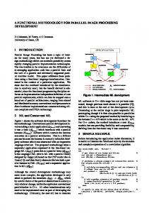
MEM
data bus
AC
IR
CTRL SHU
address bus
PC ALU
MAR
SR
Figure 1. Processor example: PARWAN level, tests are targeted at structural faults. At processor level, the functionality of the processor is used to apply the structural tests to each component at-speed. The structural component tests are delivered by processor instructions. Therefore, they must obey the constraints imposed by the instruction set. In the following two sections, we will describe the two steps included in our self-test technique: (1) component test preparation and (2) on-chip self-test. We will use a simple accumulator-based microprocessor named PARWAN [10] (Figure 1) to illustrate our methodology. PARWAN includes the following components: Arithmetic Logic Unit (ALU), Accumulator Unit (AC), Controller (CTRL), Instruction Register Unit (IR), Program Counter Unit (PC), Memory Address Register Unit (MAR), Shifter Unit (SHU), and Status Register Unit (SR). The remaining of the paper is organized as follows. Section 4 describes the software framework used for evaluating the fault coverage of self-test programs. Section 5 presents the experimental results in terms of processor fault coverage. The conclusion is drawn in Section 6.
2. Component test preparation During component test preparation, we develop tests for individual components of the processor, such as the ALU, the SHU, and the PC. Structural faults are targeted during component test generation. Component tests can either be stored or generated on-chip. If stored tests are used, component tests are loaded directly to the processor memory before the test. If tests are to be generated onchip, we characterize the test need of the component by a self-test signature, which includes the seed (S) and the configuration of a pseudo random number generator (C), as well as the number of test patterns to be generated (N). The self-test signatures, instead of actual tests, are loaded to the processor memory before the test. The self-test
signatures can be expanded on-chip into test sets using a pseudo random number generation program. Multiple self-test signatures may be used for one component, if it is necessary for increasing the fault coverage. The purpose of using self-test signatures is to reduce the time for loading the tests and the memory requirement for storing all test patterns at the same time. Notice that both self-test signatures and stored test sets can be loaded to processor memory using a low speed external tester prior to the application of tests. One of the challenges of the proposed method lies in the generation of realizable component tests. In the next two sections, we will describe the constraints on component tests imposed by the processor instruction set and the methods for modeling these constraints during test generation.
2.1 Instruction-imposed constraints Since the delivery of component tests relies on processor instructions, it is impossible to deliver some test patterns. Thus, component tests need to obey certain constraints imposed by the processor instruction set, such as validity of input values and dependency between inputs. For example, while most data inputs are constraint-free, control inputs often come with many constrains since they are determined by instruction opcodes. We will next use one component of the PARWAN processor, SHU, to illustrate the types of constraints imposed by the instruction set. A block diagram of SHU is shown in Figure 2. The input signals include data_in, in_flag, and the shifting signals from the controller. in_flag include 4 bits, v, c, z, and n, which denote overflow, carry, zero, and negative, respectively. The shifting signals includes two bits, asl and asr, which denote arithmetic-shift-left and arithmetic-shift-right. The constraints imposed by the processor instruction set can be divided into two types, depending on whether the constraint is timing-related. We define constraints which can be specified in a single time frame as spatial constraints, and constraints spanning over several time frames as temporal constraints.
in_flag (vcnz) data_in 8 4 asl asr
SHU 4 out_flag
8 data_out
Figure 2. SHU
MEM
MEM
AC
AC
AC
ALU
ALU
ALU
SHU
SHU
SHU
(a)
(b)
(c)
Figure 3. Hardware paths involved in testing the SHU (a) loading data into AC, (b) shifting, and (c) storing AC content to memory For SHU, the spatial constraints imposed by the processor instruction set include the following: 1. asl and asr cannot be both 1, 2. z and n must be consistent with data_in, and 3. v = xor(c, sign_bit(data_in)). The temporal constraints on SHU are imposed by the sequence of instructions that apply tests to SHU. The instruction sequence includes three steps. The first step is to store the data to be shifted into the accumulator (AC). This can either be done by the load accumulator instruction or any instruction that stores its result in AC. The second step is to use a shift instruction to shift the data stored in AC. The shift result cannot be stored directly to memory and has to be stored in AC temporarily. The third step is to store the AC content to memory for later analysis. The hardware paths in these three steps are shown in Figure 3. Notice that it involves three passes through SHU. Due to the possibility of aliasing, a test set with full coverage on SHU might leave certain faults undetected, if applied to SHU using instructions. To prepare tests not susceptible to the aliasing problem, temporal constraints need to be modeled during component test generation. Tupuri et al. and Vishakantaiah et al. have addressed the issue of constraint test generation in [11][12][13]. They have proposed a methodology in systematically extracting component constraints from the processor HDL description. The extracted constraints are used in generating component test vectors. The component test vectors can later be translated to processor level test vectors, which have to be applied by external testers. Such constraint extraction method, if made available, can be used in the self-test scheme proposed in this paper. However, as Wohl et al. have pointed out in [14], certain architectural constraints cannot be detected at circuit level. Therefore, the set of constraints extracted from the structural description of the processor is only a subset of the constraints imposed by the instruction set.
2.2 Constraint modeling in test generation Having described the spatial and temporal constraints imposed by the processor instruction set, we will now describe how these constraints can be modeled during component test preparation. If component tests are generated by ATPG, spatial constraints can be specified during test generation with the aid of the ATPG tool. For instance, constraint “asl and asr cannot be both 1” can be specified to the ATPG tool we are using as follows [15]: ADD ATPG FUNCTION f1 AND asl asr ADD ATPG CONSTRAINT 0 f1 The first statement defines a new variable, f1 = and(asl, asr). The second statement restricts the value of f1 to 0. As a result, asl and asr can never be both 1. As an alternative, spatial constraint can be specified with a virtual constraint circuit proposed in [11]. If random tests are used for components, random patterns can only be used on independent inputs. In the case of SHU, these would be data_in and c. Inputs such as z, n, and v can be derived from these inputs. It is inconvenient to assign random patterns to instructionrelated signals, such as the shifting signals. Therefore, they are fixed when random patterns are applied to other inputs. The fixed value of the instruction-related signals may be changed if it helps to improve the component fault coverage. For example, the shifting signals (asl and asr) can be fixed to 10, 01, or 00 while random patterns are applied to data_in and c. This corresponds to three SHU modes: left shift, right shift, and no shift. Random tests can be developed for each mode separately, until an acceptable fault coverage is achieved. As a result of component test preparation, a self-test signature is generated for each SHU mode, as shown in Table 1. Multiple self-test signatures can be used for each mode, if it is necessary for improving the fault coverage. The temporal constraints of SHU can be modeled using the three-phase sequential circuit shown in Figure 4. The three phases correspond to the three instructions for applying tests to SHU, which are loading data into AC, shifting, and storing AC content to memory (Figure 3). Notice that the data inputs and flag inputs of SHU are Table 1. Self-test signatures for SHU asr, asl fixed to 00 fixed to 01 fixed to 10
data_in, c (C1, S1, N1) (C2, S2, N2) (C3, S2, N3)
v, z, n derived derived derived
4
vc=00 4
8 SHU
0 0
SHU
8 REG
Phase 1 Loading to AC
vc=00 4
8
8 REG
Phase 2 Shifting
0/1 1/0
8
SHU
C1
0 0
8 REG
Phase 3 Storing to MEM
Figure 4. Circuit for modeling the temporal constraint of SHU only connected to the primary inputs in the first phase, in which the AC content is loaded from the memory. The data outputs of SHU are only connected to the primary outputs in the third phase, in which the test response is stored to memory. The shifting signals in these two phases are set to 0’s. The v and c flags are set to 0’s in the second and the third steps, since neither shift instructions nor store instruction can set them to 1. At any phase, the inputs to SHU must also obey the spatial constraints we have described before.
3. On-chip self-test In this section, we describe the phase of the on-chip self-test, which includes the on-chip generation of component test patterns, the delivery of component tests, and the analysis of their responses using processor instructions.
3.1 On-chip test generation If tests are chosen to be generated on-chip, we need to expand the component self-test signatures determined during component test preparation into test sets using a pseudo random number generator. Figure 5 illustrates this process. We could chose to generate the pseudo random numbers using a Linear Feedback Shift Register (LFSR), as shown in Figure 5(a). Alternatively, a more flexible and more cost-effective solution is a software LFSR, as shown in Figure 5(b). Unlike the hardware LFSR, the software LFSR is programmable and can be reused to generate any LFSR configurations without any test overhead. The configuration of the LFSR is determined by a self-test signature, which includes the characteristic polynomial of the LFSR (C), the initial state of the LFSR (S), as well as the number of test patterns to be generated (N). Multiple signatures can be used for one component, if it is necessary for improving the fault coverage.
3.2 On-chip test delivery and response collection Since the component tests are developed under the constraints imposed by the processor instruction set, it
C3
C2
D Q
D Q
D Q
New_bit Q1 Q2 (a) Hardware implementaion
Q3
Q = S Do N times begin AC