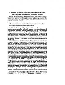
high performance and low energy consumption. The D-VLS ..... 134.perl. 147.vortex. Average. Fix128double. Fix128W4. Fix128W2. Fix128. D-VLS128-32. Fig. 4.
1
PAPER
A High-Performance/Low-Power On-chip Memory-Path Architecture with Variable Cache-Line Size Koji INOUE† , Koji KAI†† , Nonmembers, and Kazuaki MURAKAMI† , Member
SUMMARY This paper proposes an on-chip memory-path architecture employing the dynamically variable line-size (D-VLS) cache for high performance and low energy consumption. The D-VLS cache exploits the high on-chip memory bandwidth attainable on merged DRAM/logic LSIs by replacing a whole large cache line in one cycle. At the same time, it attempts to avoid frequent evictions by decreasing the cache-line size when programs have poor spatial locality. Activating only on-chip DRAM subarrays corresponding to a replaced cache-line size produces a significant energy reduction. In our simulation, it is observed that our proposed on-chip memory-path architecture, which employs a directmapped D-VLS cache, improves the ED (Energy Delay) product by more than 75 % over a conventional memory-path model. key words: cache, low power, variable line-size, merged DRAM/logic LSIs, high bandwidth
1.
Introduction
Integrating a main memory (DRAM) and processors into a single chip, or a merged DRAM/logic LSI, makes possible to exploit the high on-chip memory bandwidth provided by widening on-chip bus and on-chip DRAM array. This approach is well known as a good solution to break the memory wall problem [6][8]. Although the high on-chip memory bandwidth improves data transfer ability, still we will have a performance-gap problem between recent GHz high-speed processors and low-speed DRAM. Thus, we believe that it will be needed to employ high-speed on-chip caches even if the main memory and the processors are integrated. For merged DRAM/logic LSIs having cache memory, we can exploit the high on-chip memory bandwidth by replacing a whole cache line at a time[2][9][11]. This approach tends to increase the cache-line size if we attempt to exploit the attainable high bandwidth. A large cache-line size gives a benefit of prefetching effect if programs have rich spatial locality. However, it will bring the following disadvantages with poor spatial locality: 1. a number of conflict misses will take place due to frequent evictions, Manuscript received Department of Computer Science and Communication Engineering, Kyushu University, 6–1 Kasuga-koen, Kasuga, Fukuoka 816-8580 Japan. †† Institute of Systems & Information Technologies / KYUSHU, 2-1-22 Momochihama, Sawara-ku, Fukuoka 8140001 Japan. †
2. as the result, a lot of energy at the on-chip DRAM (main-memory) will be wasted by a number of DRAM accesses, and
3. activating the wide on-chip bus and the DRAM array will also dissipate a lot of energy. Employing set-associative caches is a well known approach to avoid the first and second disadvantages, because it can improve cache-hit rates. Since increasing the cache associativity makes cache access time longer, however, it might worsen the memory system performance. In addition, still we will have the third disadvantage. In order to resolve all of the disadvantages without cache access time overhead, we have proposed a dynamically variable line-size cache (D-VLS cache) architecture for merged DRAM/logic LSIs [3]. The D-VLS cache can exploit the high on-chip memory bandwidth by means of larger cache lines. At the same time, it can alleviate the negative effects of the larger cacheline size by partitioning the large cache line into multiple small cache lines (sublines). Activating only the DRAM subarray(s) corresponding to the replaced subline(s) makes a significant energy reduction for accessing to the main memory. Appropriate cache-line sizes, or the number of sublines to be involved in cache replacements, are determined by special hardware assists at run time. In the paper [3], we have evaluated only the performance improvements achieved by the D-VLS cache, and have compared it with conventional directmapped caches having fixed various cache-line sizes and a set-associative cache having a small cache-line size. This paper focuses on the on-chip memory-path architecture employing the D-VLS cache, and compares it with conventional set-associative caches having a large cache-line size. In addition, we evaluate not only performance but also energy consumption for accessing to the on-chip main-memory. The rest of this paper is organized as follows. Section 2 briefly introduces the concept and organization of a D-VLS cache. Section 3 presents some simulation results and discusses the performance/energy efficiency of the D-VLS cache. Section 4 describes related work. Section 5 concludes this paper.
2 Cache
Cache
Processor Load/Store Data
Address
32-byte
64-byte Line
Line
0 4
1
2
3
Main Memory (a) Replace with a Minmum Line
0
1
Tag
2
Index
SA
Offset
MUX
reference-flag
3
Line-Size Specifier (LSS)
Main Memory (b) Replace with a Medium Line
Cache
next current line-size line-size
Tag
Data
32Bytes
D-VLS Cache
32Bytes
32Bytes
32Bytes
Line-Size Determinator (LSD)
Legend 128-byte Line
MUX
0
1
2
Main Memory (c) Replace with a Maxmum Line
Fig. 1 ments
Hit / Miss?
3
data transfer occurs
no data transfer occurs
Three Different Cache-Line Sizes on Cache Replace-
2.
Dynamically Variable Line-Size Cache
2.1
Concept and Principle
In the D-VLS caches, an SRAM (cache) cell array and a DRAM (main memory) cell array are divided into several subarrays. Data transfer for cache replacements is performed between corresponding SRAM and DRAM subarrays. Figure 1 shows the construction of a direct-mapped D-VLS cache having three cache-line sizes. If programs have rich spatial locality, the D-VLS cache chooses the largest cache-line size for cache replacements, as shown in figure 1 (c), in order to obtain prefetching effects aggressively. In this case, all of the DRAM subarrays and on-chip buses are activated. Contrarily, if programs have poor spatial locality, the cache attempts to reduce unnecessary evictions caused by the large cache line by partitioning it into multiple small cache lines (sublines). In this case, only a few number of sublines are replaced, as shown in figure 1 (a) or (b). Activating the DRAM subarrays and the on-chip buses corresponding to the replaced sublines can reduce the energy consumption for accessing to the main memory. The construction of a direct-mapped D-VLS cache having three cache-line sizes, which will be explained in the next section, is similar to that of a conventional 4-way set-associative cache having the smallest cache-line size. However, the conventional 4-way setassociative cache has four locations where a cache line can be placed, while the direct-mapped D-VLS cache has only one location. Since the D-VLS cache attempts to avoid cache conflicts without increasing associativ-
Main Memory
SA : Subarray
Fig. 2
Block Diagram of a Direct-Mapped D-VLS Cache
ity, it can retain first cache-access time (i.e., cache hit time) of conventional direct-mapped caches [3]. In summary, the D-VLS cache exploits effectively the high on-chip memory bandwidth according to the characteristics of memory-reference behavior, and brings the following effects. 1. Performance improvements by achieving higher cache-hit rate without cache access time overhead. 2. Energy reduction for main memory accesses by improving cache-hit rate (i.e., decrease of the total number of main memory accesses). 3. Energy reduction for main memory accesses by selective on-chip DRAM activation according to small cache-line sizes to be replaced. 2.2 Organization The effectiveness of the D-VLS cache depends largely on that how much the cache can choose adequate cacheline sizes to the amount of spatial locality in programs. The D-VLS cache optimizes its cache-line size based on recently observed memory-reference behavior. Figure 2 illustrates the block diagram of a directmapped D-VLS cache with four subarrays. In case that the subarray has 32-byte width, the candidates of cache-line size are 32 bytes, 64 bytes, and 128 bytes. The D-VLS cache has the following special hardware for run-time line size optimization. • A reference-flag bit per 32-byte cache line : This flag bit records that whether the corresponding minimum cache line has been referenced by the processor, or not, since it was filled into the cache. • A line-size specifier (LSS) per cache-sector : This specifies a cache-line size corresponding to the cache-sector which is formed by SRAM subarray entries
INOUE et al: A HIGH-PERFORMANCE/LOW-POWER ON-CHIP MEMORY-PATH ARCHITECTURE WITH VARIABLE CACHE-LINE SIZE
3
having the same cache-index. The cache replacement is performed according to the cache-line size specified by the LSS. • Line-size determiner (LSD) : On every cache look-up, the LSD determines the state of the line-size specifier (LSS) by using the reference-flag bits in the referenced cache-sector and tag comparison results. The detail of the D-VLS cache behavior and an algorithm to optimize the cache-line size have been described in [3]. 3.
Evaluation
In this section, we evaluate performance/energy efficiency of the D-VLS cache. We refer to the conventional caches and the D-VLS cache as follows † : • Fix128 : a 16 KB conventional direct-mapped cache having fixed 128-byte cache lines. • Fix128W2 : a 16 KB conventional two-way setassociative cache having fixed 128-byte cache lines. • Fix128W4 : a 16 KB conventional four-way setassociative cache having fixed 128-byte cache lines. • Fix128double : a 32 KB conventional directmapped cache having fixed 128-byte cache lines. • D-VLS128-32 : a 16 KB direct-mapped dynamically variable line-size cache having 32-byte, 64byte, and 128-byte cache lines. For each cache, we measured cache-miss rates and cache-replace counts for benchmark programs: three programs from the SPEC92 benchmark suite with reference inputs, and seven integer programs with training inputs and four floating-point programs with test inputs from the SPEC95 benchmark suite [10]. In our simulation, all programs are compiled by GNU CC with the “–O2” option, and are executed on an Ultra SPARC architecture. We have made a trace-driven simulator for the D-VLS cache. The address traces as input of the cache simulator have been captured by the QPT[1]. 3.1
Simulation Results
Table 1 shows the breakdown of cache-replace counts of the D-VLS cache having 32-byte, 64-byte, and 128-byte lines (D-VLS128-32). The last line, showed as “Ave. of Line Size”, means that the average cache-line size per cache miss. As cache replacements on conventional caches, Fix128, Fix128W2, Fix128W4, Fix128double, are always performed with 128-byte lines, the average cache-line size is 128 bytes. † It is assumed that all of set-associative caches employ write-back policy and LRU algorithm for replacements.
On the other hand, the average cache-line size of the D-VLS cache depends on the characteristics of memory reference behavior in programs, because the cache attempts to optimize its cache-line size according to the amount of spatial locality. In order to explain the results of the table 1, we use figure 3 that is the simulation results for cachemiss rate of the D-VLS128-32, and 16 KB conventional direct-mapped caches each of which has one of 32 bytes (Fix32), 64 bytes (Fix64), and 128 bytes (Fix128) fixed cache-line size. For each benchmark, simulation results are normalized to the miss rate produced by the conventional cache with the best cache-line size. As shown in figure 3, the best cache-line size is highly applicationdependent. In a number of benchmarks, however, the D-VLS cache gives nearly equal or lower miss rates than the conventional cache with the best cache-line size. For example, we can see from figure 3 that 026.compress seems to prefer smaller cache-line size for avoiding frequent evictions. Table 1 shows that the D-VLS cache attempts to use smaller cache-line size for 026.compress, and the average cache-line size is 34.69 bytes. In contrast, the larger cache-line size gives a significant improvement on 052.alvinn. In this case, the D-VLS cache chooses aggressively larger cache-line size in order to exploit the rich spatial locality, as shown in table 1, and the average cache-line size is 90.22 bytes. Table 2 shows cache-miss rate of all benchmark programs. For some programs, 052.alvinn, 134.perl, 147.vortex, 101.tomcatv, and 104.hydro2d, the D-VLS cache can achieve almost all the same or lower miss rate than the double-size conventional direct-mapped cache (Fix128double). However, increasing associativity produces much better results. In average, the cache-miss rate improvement produced by the conventional fourway set-associative cache (Fix128W4) is about 68 %, while that produced by the D-VLS cache is 28 %, from the conventional direct-mapped cache having 128-byte lines (Fix128). 3.2 Performance 3.2.1 Performance Model Cache-miss rate is one of the most popular metric of cache performance. As increasing cache access time gives great impact to total execution time, however, we use average memory access time (AM AT ) as performance metric. AM AT is an average latency required by the memory system to serve a memory reference from the processor, and can be expressed as follows: AM AT = HT + (M R × M P ) = HT + M R × 2 × (DRAM stup + • AM AT : Average Memory Access Time [ns]
LS ) Bandwidth
4 Table 1
Replace Counts with each Cache-Line Size of the D-VLS Cache
Line Size
026.compress
072.sc
052.alvinn
099.go
124.m88ksim
126.gcc
130.li
32 bytes 64 bytes 128 bytes
3,164,502 243,979 14,498
1,038,520 492,007 352,181
11,546,415 1,465,880 18,806,730
6,445,160 1,724,674 389,746
317,746 53,858 68,353
10,092,540 3,463,487 1,468,861
1,190,072 426,488 189,570
Ave. of Line Size
34.69 B
58.32 B
90.22 B
42.82 B
50.83 B
48.76 B
49.63 B
Line Size
132.ijpeg
134.perl
147.vortex
101.tomcatv
102.swim
103.su2cor
104.hydro2d
32 bytes 64 bytes 128 bytes
3,530,649 1,179,064 1,246,695
7,987,886 5,250,134 3,849,457
19,805,372 3,593,130 1,416,595
23,539,313 2,608,352 2,650,269
32,465,163 4,163,613 884,142
15,340,954 6,701,837 3,315,895
3,784,227 860,802 6,175,600
Ave. of Line Size
58.43 B
63.46 B
42.11 B
43.73 B
37.81 B
53.01 B
89.34 B
1.792
1.775
1.633
Table 2
Cache Miss Rate with Large Cache-Line Size
1.50 1.40
Normalized Miss Rate
1.30 1.20 1.10
1.00 0.90 0.80 0.70 0.60 072.sc 124.m88ksim 026.compress 099.go 126.gcc
130.li
134.perl 132.ijpeg 147.vortex
Integer Benchmarks 2.031
1.546 1.891
2.931
1.638
1.50 1.40
FIX32 FIX64 FIX128 D-VLS128-32
Normalized Miss Rate
1.30
Benchmark
Fix128
Fix128 W2
Fix128 W4
Fix128 double
D-VLS 128-32
026.compress 072.sc 052.alvinn 099.go 124.m88ksim 126.gcc 130.li 132.ijpeg 134.perl 147.vortex 101.tomcatv 102.swim 103.su2cor 104.hydro2d Ave. of normalized miss rate to Fix128
0.1871 0.0371 0.0224 0.1024 0.0202 0.0611 0.0341 0.0244 0.0542 0.0505 0.0633 0.2612 0.2600 0.0481
0.1755 0.0285 0.0087 0.0695 0.0045 0.0344 0.0203 0.0048 0.0230 0.0292 0.0182 0.3007 0.0840 0.0217
0.1711 0.0263 0.0080 0.0302 0.0028 0.0254 0.0182 0.0036 0.0105 0.0195 0.0062 0.3137 0.0242 0.0179
0.1634 0.0276 0.0175 0.0541 0.0068 0.0349 0.0226 0.0068 0.0295 0.0307 0.0546 0.1016 0.2396 0.0259
0.1724 0.0465 0.0166 0.0638 0.0153 0.0526 0.0358 0.0175 0.0286 0.0374 0.0578 0.1419 0.0758 0.0295
1.000
0.479
0.315
0.583
0.715
1.20
to a constant time regardless of cache-line sizes. In this evaluation, we assume that the DRAM stup and the LS Bandwidth are 50 ns and 10 ns, respectively. In addition, it is also assumed that all contents of the replaced cache line are dirty. In other words, two DRAM accesses with a cache-line size, one for write-back and one for fill, will take place on each cache miss.
1.10
1.00 0.90 0.80 0.70 0.60 052.alvinn
101.tomcatv 103.su2cor 102.swim 104.hydro2d
3.2.2 Average Memory Access Time
Floating-Point Benchmarks
Fig. 3
Cache Miss Rate of Direct-Mapped Caches
• HT : cache Hit Time [ns] • M R: cache Miss Rate • M P : cache Miss Penalty [ns] • DRAM stup : DRAM start-up time [ns] • LS : cache Line-Size [byte] • Bandwidth : memory Bandwidth between the cache and DRAM
Here, since merged DRAM/logic LSIs can provide the high on-chip memory bandwidth, the M P becomes
In order to find cache-hit time of the conventional caches, we have used the CACTI model† [13]. The CACTI estimates the cache-access time with a detail analysis of several components, for example, sense amplifiers, output drivers, and so on. Based on the CACTI, we assumed that the cache-hit time of Fix128, Fix128W2, Fix128W4, and Fix128double are 3.510 ns, 6.695 ns, 8.421 ns, and 4.115 ns, respectively. A direct-mapped D-VLS cache does not have any †
In this simulation, we have assumed that the process rule parameter, address width, and output-data width are 0.5 um, 30 bits, and 32 bits, respectively.
INOUE et al: A HIGH-PERFORMANCE/LOW-POWER ON-CHIP MEMORY-PATH ARCHITECTURE WITH VARIABLE CACHE-LINE SIZE
5 1.60
3.3 Energy Consumption for Accessing The On-chip Main Memory
Normalized Miss Rate
1.40 1.20
3.3.1 Energy Model
1.00 0.80 0.60 0.40 0.20 0.00
072.sc 099.go 126.gcc 052.alvinn 124.m88ksim 026.compress
1.60
Fix128 Fix128W2 Fix128W4 Fix128double D-VLS128-32
1.40 Normalized Miss Rate
132.ijpeg 130.li
1.20
1.00 0.80 0.60 0.40
We believe that the energy consumption at the on-chip main memory depends largely on that how much the on-chip DRAM and the on-chip bus are activated. In order to simplify this evaluation, we assume that the on-chip DRAM does not consume any energy while it is inactivated. This means that we do not consider the energy consumption for DRAM refresh. Thus, for on-chip memory-path architectures with a conventional cache, the energy consumption depends only on total number of main memory accesses. In other words, only cachemiss rates affect the energy consumption for main memory accesses. Since the D-VLS cache activates only the DRAM subarrays corresponding to replaced sublines, the energy consumption for accessing to the on-chip main memory depends not only on cache-miss rates but also on cache-line sizes (i.e., the number of sublines to be involved in cache replacements). Accordingly, the energy consumption at the on-chip main memory (E) can be expressed as follow:
0.20 0.00
134.perl
101.tomcatv 103.su2cor 147.vortex 102.swim 104.hydro2d
Average
Benchmark Programs
Fig. 4
Normalized Average Memory Access Time
cache-hit time overhead from a conventional directmapped cache, because the hardware components to optimize the cache-line size do not appear on cache critical paths [3]. Thus, in this evaluation, we have assumed that the cache-hit time of the direct-mapped D-VLS cache (D-VLS128-32) is the same as that of the conventional direct-mapped cache with 128-byte lines (Fix128). Figure 4 depicts the average memory access time for benchmark programs. All results are based on the cache-miss rates reported in the section 3.1 and the cache-hit time from the CACTI. All results are normalized to Fix128. Though increasing cache associativity (Fix128W2, Fix128W4) makes great improvement of cache-miss rate, as showed in earlier, their average memory access time are longer than that of the directmapped cache (Fix128) due to long cache-hit time. The D-VLS cache has no cache-hit time overhead, so that its miss-rate improvement appears on the average memory access time directly. In average, the D-VLS cache produces about 20 % performance improvement from the direct-mapped conventional cache (Fix128). This improvement is almost all the same as that achieved by the double-size conventional cache having 128-byte lines (Fix128double).
E=
�
RepCount(n) × Esubarray × n/32bytes,
N
N = {n|n = 32bytes, 64bytes, 128bytes}. Here, n is the cache-line size. Esubarray is the energy consumption for two main memory accesses, one for write-back and one for fill, to a 32-byte width DRAM subarray. RepCount(n) means the total number of replace counts with cache-line size n. For the conventional caches having 128-byte fixed lines, Fix128, Fix128W2, Fix128W4, and Fix128double, there is no energy consumption with 32-byte and 64-byte lines (RepCount(32bytes) = 0, and RepCount(64bytes) = 0). 3.3.2 Energy Consumption Figure 5 depicts the energy consumption for accessing to the on-chip main-memory. All results are normalized to the conventional direct-mapped cache having 128-byte lines (Fix128). As explained earlier, the energy consumption for conventional caches depends only on cache-miss rates. In average, the conventional fourway set-associative cache (Fix128W4), which produces the best cache-miss rate, reduces the energy consumption about 68 % from Fix128. Although the cache-miss rates of D-VLS cache are much higher than those of Fix128W4, the cache also produces a significant advantage of energy consumption. By improving cachemiss rates, the cache reduces the total number of main memory accesses by about 28 %. In addition, about 57
6
Normalized ED Product (E * AMAT)
Normalized Energy Consumption (E)
1.20
1.00
1.20
1.00
0.80
0.60
0.40
0.20
0.80
0.60
0.40
0.20
0.00
072.sc 099.go 126.gcc 052.alvinn 124.m88ksim 026.compress
0.00
132.ijpeg
072.sc 099.go 126.gcc 052.alvinn 124.m88ksim 026.compress
130.li
Benchmark Programs
1.00
1.60
Normalized ED Product (E * AMAT)
Normalized Energy Consumption (E)
Benchmark Programs
Fix128 Fix128W2 Fix128W4 Fix128double D-VLS128-32
1.20
132.ijpeg 130.li
Fix128 Fix128W2 Fix128W4 Fix128double D-VLS128-32
1.40 1.20
1.00
0.80
0.60
0.40
0.80 0.60 0.40 0.20
0.20
0.00 0.00
134.perl
Fig. 5 and bus
101.tomcatv 103.su2cor 147.vortex 102.swim 104.hydro2d Benchmark Programs
Average
3.4
Energy-Delay Product
In order to evaluate both of performance and energy improvements achieved by the D-VLS cache at the same time, we compare the energy-delay products of the proposed cache (D-VLS128-32) and the conventional caches (Fix128, Fix128W2, Fix128W4, and Fix128double). Figure 6 shows the calculation results. Again, all results are normalized to Fix128. We can see from figure 6 that the most effective one of the conventional caches is the four-way setassociative cache (Fix128W4). However, the advantage of low energy consumption achieved by lower cache-miss rate is negated by the slower cache access on Fix128W4. Contrarily, the performance improvement given by the first cache access on the 32 KB conventional directmapped cache (Fix128double) is negated by the higher
101.tomcatv 103.su2cor 147.vortex 102.swim 104.hydro2d
Average
Benchmark Programs
Fig. 6
Normalized Energy Consumption at On-chip DRAM
% energy reduction for activating the on-chip bus and DRAM can be achieved by means of the variable cacheline size (i.e., selective on-chip DRAM activation). The total energy reduction is about 70 %.
134.perl
Normalized ED Product (E × AM AT )
energy consumption caused by the higher cache-miss rate and dealing with the 128-byte large-lines. Since the D-VLS cache can avoid the frequent evictions without access-time overhead, it does not have this kind of negations. In average, the D-VLS cache produces more than 75 % improvement of performance/energy efficiency from Fix128. 4.
Related Work
Saulsbury et al.[9] and Wilson et al.[11] discussed cache architectures having large cache-line size (512 bytes) with high on-chip memory bandwidth. They tried to avoid frequent cache conflicts, occurred by the large cache lines, by increasing cache associativity. As the D-VLS cache resolves the conflict problem using variable cache-line size, first access of direct mapped cache can be maintained. The cache architectures having run-time line-size optimization mechanisms were proposed in [4] [5] [12]. They focused on only performance improvement achieved by the variable cache-line size. While our goal is to bring out the potential ability of merged
INOUE et al: A HIGH-PERFORMANCE/LOW-POWER ON-CHIP MEMORY-PATH ARCHITECTURE WITH VARIABLE CACHE-LINE SIZE
7
DRAM/logic LSIs by solving the larger cache-line-size disadvantages from both of performance and energy point of view. Ohsawa et al. [7] proposed some methods to reduce energy consumption of on-chip DRAM. They tried to reduce energy consumption for DRAM refresh by optimizing the DRAM refresh count. Against their study, our interest is to make energy reduction at the widen on-chip bus and DRAM by avoiding unnecessary DRAM accesses for cache replacements. 5.
Conclusions
In this paper, we have evaluated both of the performance and energy consumption of an on-chip memorypath architecture employing the dynamically variable line-size (D-VLS) cache. In our simulation, it is observed that a directmapped D-VLS cache having 32-byte, 64-byte, and 128byte lines (D-VLS128-32) improves the average memory access time by about 20 %, compared with a conventional direct-mapped cache with 128-byte lines (Fix128). This improvement is almost all the same as that achieved by a conventional double-size directmapped cache with 128-byte lines (Fix128double). In addition, the D-VLS cache can reduce about 70 % energy consumption for accessing to the on-chip mainmemory by reducing the total number of DRAM accesses and activating only DRAM subarrays corresponding to optimized cache-line sizes. Finally, the D-VLS cache improves the ED (Energy Delay) product by more than 75 % from the Fix128. This improvement is about 10 % better than that of a conventional four-way set-associative cache having 128-byte lines (Fix128W4) which produces the best result of the conventional caches. This paper has not considered the energy consumption for cache accesses. Moreover, we have assumed that there is no energy consumption at the on-chip DRAM while it is inactivated. In fact, some energy should be dissipated for DRAM refresh operations. Accordingly, it is our future work to evaluate the total energy consumption of whole on-chip memory-system.
versity of Wisconsin - Madison. [2] Inoue, K., Koji, K., and Murakami, K., “High Bandwidth, Variable Line-Size Cache Architecture for Merged DRAM/Logic LSIs,” IEICE Transactions on Electronics, Vol.E81-C, No.9, pp.1438–1447, Sep. 1998. [3] Inoue, K., Koji, K., and Murakami, K., “Dynamically Variable Line-Size Cache Architecture for Merged DRAM/Logic LSIs,” IEICE Transactions on Electronics, Vol.E83-D, No.5, pp.1048–1057, May 2000. [4] Johnson, T. L., Merten, M. C, and Hwu, W. W., “Runtime Spatial Locality Detection and Optimization,” Proc. of the 30th Annual International Symposium on Microarchitecture, pp.57–64, Dec. 1997. [5] Kumar, S. and Wilkerson, C., “Exploiting Spatial Locality in Data Caches using Spatial Footprints,” Proc. of the 25th Annual International Symposium on Computer Architecture, pp.357–368, June 1998. [6] Murakami, K., Shirakawa, S., and Miyajima, H., “Parallel Processing RAM Chip with 256Mb DRAM and Quad Processors,” 1997 ISSCC Digest of Technical Papers, pp.228– 229, Feb 1997. [7] Ohsawa, T., Kai, K., and Murakami, K., “Optimizing the DRAM Refresh Count for Merged DRAM/Logic LSIs,” Proc. of 1998 International Symposium on Low Power Electronics and Design, pp.82–87, Aug. 1998. [8] Patterson, D., Anderson, T., Cardwell, N., Fromm, R., Keeton, K., Kozyrakis, C., Thomas, R., and Yelick, K., “Intelligent RAM (IRAM): Chips that remember and compute,” 1997 ISSCC Digest of Technical Papers, pp.224–225, Feb 1997. [9] Saulsbury, A., Pong, F., and Nowatzyk, A., “Missing the Memory Wall: The Case for Processor/Memory Integration,” Proc. of the 23rd Annual International Symposium on Computer Architecture, pp.90–101, May 1996. [10] SPEC (Standard Performance Evaluation Corporation), URL: http://www.specbench.org/osg/cpu92, http://www.specbench.org/osg/cpu95. [11] Wilson, K. M. and Olukotun, K., “Designing High Bandwidth On-Chip Caches,” Proc. of the 24th Annual International Symposium on Computer Architecture, pp.121–132, June 1997. [12] Vleet, P. V., Anderson, E., Brown, L., Baer, J., L., and Karlin, A., “Pursuing the Performance Potential of Dynamic Cache Line Sizes,” Proc. of 1999 IEEE International Conference on Computer Design : VLSI in Computer & Processors, pp.528–537, Oct. 1999. [13] Wilton, S. J. E. and Jouppi, N. P., “CACTI:An Enhanced Cache Access and Cycle Time Model,” IEEE Journal of Solid-State Circuits, vol.31, no.5, pp.677–688, May 1996.
Acknowledgments We thank Hiroto Yasuura who gave us advice on laboratory seminar. We also thank Mizuho Iwaihara Kyushu Univ. and PPRAM project team. This research was supportd in part by the Grant-in-Aid for Scientific Research (A) contracts 09358005, 11308011, and 12358002. References [1] Hill, M. D., Larus, J. R., Lebeck, A. R., Talluri, M., and Wood, D. A., “WARTS: Wisconsin Architectural Research Tool Set,” http://www.cs.wisc.edu/ ˜larus/warts.html, Uni-
Koji Inoue was born in Fukuoka, Japan in 1971. He received the B.E. and M.E. degrees in computer science from Kyushu Institute of Technology, Japan in 1994 and 1996, respectively. He entered Yokogawa Electric Corporation in 1996. In 1999, he joined Halo LSI Design & Technology, Inc., NY, as a circuit designer. Currently he is a Ph.D. degree in Department of Computer Science and Communication Engineering, Grad-
8
uate School of Information Science and Electrical Engineering, Kyushu University. His research interests processor and cache architectures. He is a member of IPSJ.
Koji Kai received the B.E. and M.E. degrees in computer science from Kyushu University, Fukuoka, Japan, in 1989 and 1991, respectively. He has belonged to Matsushita Electric Industrial, Co., Ltd. since 1991. From 1966 to 2000, he was working for Institute of Systems & Information Technologies/KYUSHU as a researcher. He is presently engaged in the development of a system LSI at Matsushita’s Information Technology System LSI Development Center, Fukuoka, Japan. His research interests include processor architectures, design methods of VLSI systems and hardware/software co-design. He is a member of Information Processing Society of Japan and IEEE Computer Society.
Kazuaki Murakami was born in Kumamoto, Japan in 1960. He received the B.E., M.E., and Ph.D. degrees in computer science and engineering from Kyoto University, Japan in 1982, 1984, and 1994, respectively. From 1984 to 1987, he worked for the Fujitsu Limited, where he was a Computer Architect of the mainframe computers. In 1987, he joined the Department of Information Systems of Kyushu University, Japan, and then was an Associate Professor of the Department. Since 1996, he was an Associate Professor of the Department of Computer Science and Communication Engineering. He is currently a Professor of the Department of Information Science. His original research area was ILP (instruction-level parallel) processors, and in 1987, he proposed one of the first superscalar architectures. His current research focuses on the area of designing and exploiting new computer systems based on advanced VLSI and parallel-processing technologies. In 1994, he started PPRAM (Parallel Processing Random Access Memory) project and is now leading the design and implementation of PPRAM chips. He is also working on another research project, called SmartCore, which aims at developing an application-domain-specific, user-customizable logic/processor core. He is a member of the ACM, the IEEE, the IEEE Computer Society, the IPSJ (Information Processing Society of Japan), and the JSIAM (Japan Society for Industrial and Applied Mathematics).