272
Journal of Power Electronics, Vol. 5, No. 4, October 2005
JPE 5-4-4
A New Control Scheme for a Class-D Inverter with Induction Heating Jar Application by Constant Switching Frequency Won-Suk Choi†, Nam-Ju Park*, Dong-Yun Lee* and Dong-Seok Hyun*
†*
Dept. of Electrical Engineering, HanYang University, HaengDang Dong, SungDong Gu, 133-791, Seoul, Korea
ABSTRACT In this paper, a simple power control scheme for a constant frequency Class-D inverter with a variable duty cycle is proposed. It is more suitable and acceptable for high- frequency induction heating (IH) jar applications. The proposed control scheme has the advantages of not only wide power regulation range but also ease of control output power. Also it can achieve a stable and efficient Zero-Voltage-Switching (ZVS) in a whole load range. The control principles of the proposed method are described in detail and its validity is verified through simulated and experimental results on 42.8kHz IGBT for induction heating rated on 1.6kW with constant frequency variable power. Keywords: IH-Jar(Induction Heating-Jar), PFM(Pulse Frequency Modulation), PWM(Power Width Modulation), Class-D Inverter, ZVS(Zero-Voltage-Switching)
1. Introduction Recently with the development of power semiconductor devices, new circuit techniques and control schemes, research on high frequency circuits and advanced power devices such as MOSFETs and IGBTs etc. have been many performed for high power applications [1]-[15]. The various resonant inverters using power devices such as MOSFETs and IGBTs offer reduced switching loss by using soft-switching technique and offer attractive possibilities in developing higher frequencies of operation, higher efficiency, a smaller size and lighter weight. Induction heating (IH) has been a part of high power applications and widely used in industrial fields, office Manuscript received October 28, 2004; revised August 25, 2005 Corresponding Author:
[email protected] Tel: +82-2-2290-0341, Fax: +81-2-2297-1569, Hanyang Univ. * Dept. of Electrical and Electronics Eng., Hanyang Univ. †
Copyright (C) 2006 NuriMedia Co., Ltd.
automation fields and electric home appliances. In particular, IH-Jar, which is an application of IH is used in home appliances such as cookers [3]-[5]. The requirements for IH applications are as follows: - High frequency switching - High efficiency - Power factor close to unity - Low cost - Wide load range - Reliability High-frequency Class-D inverters have become very popular and become more and more widely used in various applications. It must be effectively selected according to the application in order to meet the inverter requirements under a high frequency switching operation due to load specifications. An important goal of power control is to achieve an efficient and useful product. Generally, most induction heating applications use a variable frequency scheme to control output power [5]-[6]. The frequency modulation control is a basic method that is applied against the variation of load or line frequency.
273
A New Control Scheme for a Class-D Inverter with …
However, pulse frequency modulation control causes many problems since the switching frequency has to be varied over a wide range to accommodate the worst combinations of load and line. The major disadvantage of this method is the large frequency range required for output power control over a wide range. For operations below resonance, filter components are large because they must be designed for the low frequency range. For operations above resonance, fast switching devices are required to maintain control at the upper frequency range. It is apt to produce audible noise when two or more inverters are operated at the same time with different switching frequency. Besides, the soft switching operating area of the ZVS-PFM high frequency inverter is relatively narrow under a pulse frequency modulation strategy. Keeping the switching frequency constant and controlling it by pulse width modulation (PWM) are obvious ways to avoid the problems of variable frequency control [7]-[11]. Therefore, Class-D inverter topologies using a PWM chopper at the input, phase-shifted PWM control, PWM technique, current mode control and a variable resonant inductor or capacitor have been proposed. Constantswitching frequency operation supposes that every inverter in the application is operating at the same frequency, making it necessary to control power without frequency variations. That is highly desired for optimum design of the output smoothing and noise filters. However these control requirements and operating characteristics have an added complexity due to the fixed frequency of switching which limits their performance [12]. And if the system has a phase-shift PWM control, the ZVS does not exist at light load [13]-[14]. This paper deals with a simple power control scheme of constant frequency variable power (CFVP) for a Class-D inverter with induction heating jar application. When the inverter operates at a fixed switching frequency higher than its resonant frequency, it can maintain the ZVS operation in the whole load range. Thus switching losses, EMI, are decreased. By adjusting the duty cycle of the fixed frequency, the output power is simply controlled in wide load range (10%-100% load). The advantages of this inverter control scheme are simple configuration and wide power regulation range. It can improve the power control and elevate control response performance. Also the switches always guarantee
Copyright (C) 2006 NuriMedia Co., Ltd.
zero-voltage-switching (ZVS) from light to full load and the filter is easy to design due to the use of constant switching frequency. The proposed power control scheme and the principles of the Class-D inverter are explained in detail. Theoretical analysis, simulation and experimental results verify the validity of the Class-D inverter with the proposed PWM control scheme.
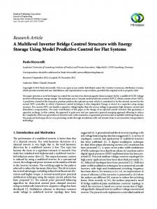
2. Class-D Series Resonant Inverter [1] 2.1 Circuit description The Class-D inverter will be generally used to energize the induction coil to generate high-frequency magnetic induction between the coil and the cooking vessel, high-frequency eddy currents and finally heat in the vessel bottom area. Class-D inverters take the energy from the mains voltage. The DC voltage is converted again into a high-frequency AC voltage by a Class-D inverter. Then the inverter supplies the high-frequency current to the induction coil.
S1
D1
Vd D2
Cr /2
1
Leq S2
Fig. 1
Cs
Cs
2
Req Cr /2
Class-D inverter system for IH jar application
Fig. 1 shows a Class-D inverter system for a induction heating jar. The Class-D inverter consists of two switches S1, S2 with anti-parallel diodes D1, D2 using IGBT, two resonant capacitors Cr/2 and an induction coil that consists of a series combination of resistance Req and inductance Leq. One of the main advantages of the half-bridge inverter is low voltage across the switch that is equal to the supply voltage. Thus, compared with other topologies (Class-E, Quasi-resonant inverter etc.) for induction heating applications, it is suited for high-voltage applications [1]. The utility DC input voltage of 311V is directly supplied into an inverter and S1, D1 and S2, D2 are alternately used to administer high frequency current to the induction coil.
274
Journal of Power Electronics, Vol. 5, No. 4, October 2005
Leq
Req
S1
IL
Vd
Vd
S2
Cr
S1
Equivalent circuit
S2
Dead Time
π
ωs t
2π
S2
ωs t
0 VS
Vdc
0 t t’ t 0 0 1
Cs1, Cs2
Mode 1
Fig. 3
IL t2 t2’
D1
-
Cr /2
S1
D1
S2
D2
Vd Cr /2
S1 Mode 2
t3
ωs t
t4
Cs1, Cs2
Mode 3
D2
Cs1
S2 Mode 4
Theoretical waveforms of the Class-D inverter
Fig. 3 described the operation mode including switching signals and inverter output voltage Vs and current IL waveforms. As shown in Fig. 3, if the switches are operated above resonant frequency, the series resonant circuit represents an inductive load and the load current IL lags behind the output voltage Vs, Therefore, load current IL flows in the order of Cs1,Cs2→D1→S1→Cs1,Cs2→D2→S2. At this time, the switching losses do not occur at turn-on because the switches are turned on at zero voltage. The Class-D inverter with the PWM control scheme is explained in detail when it is applied to the IH-jar. Fig. 3 and Fig. 4 illustrates the steady-state theoretical waveforms and operation modes of the Class-D inverter. The steady-state analysis of the Class-D inverter is based on the following assumptions.
Copyright (C) 2006 NuriMedia Co., Ltd.
D2
Cs2
S1
D1
Vd D2
+
Cr /2
Cs2
+
Cr /2
Cr /2
-
D1
Cr /2
S2
D2
Cs1
Leq ILeq R eq Cs2
+ -
Cr /2
Cr /2
Mode 4 (t2-t2’)
Cs1
+ -
Mode 5 (t2’-t3) Fig. 4
S1 Vd
-
Leq ILeq R eq Cs2
Cs1
Leq ILeq R eq
Mode 2 (t0’-t1)
Mode 3 (t1-t2)
S2
0
Cs2
+
Leq ILeq R eq
Vd
Fig. 2 represents the equivalent circuit model of a Class-D inverter. In particular, two switches are operated at square wave with suitable dead time between the two driving commands. The Class-D inverter is operated above the resonant frequency, which means that the switches are turned-off while carrying current. S1
D2
Cs1
Leq ILeq R eq
Mode 1 (t0-t0’)
Z Fig. 2
D1
S1
Cr /2 Vd Cr /2
S2
D1
Cs1
Leq ILeq R eq Cs2
+ -
Cr /2
Cr /2
Mode 6 (t3-t4)
Operation modes of the Class-D inverter
- All components are ideal. - Input voltage of the DC link is constant in one switching cycle. - Effects of the parasitic capacitances of the switch are neglected. - Load current is nearly sinusoidal because the large load quality factor (Q) is high enough. 2.2 Circuit Operation and Analysis of Mode 1, 2, 3 At t=t0, Cs1 and Cs2 begin to resonate with energy in the inductor Leq. The load current iLeq is transferred from S2 to capacitor Cs1 and Cs2. At t=t0’, the load current, iLeq flows through Leq→D1→Vd→Req, thus switch S1 is turned on under the ZVS condition at t1. These modes are continuous in circuit operation and provide the same circuit connection with its actual direction of current flow shown in Mode 1, Mode 2 and Mode 3 of Fig. 4. At this point, according to the Thevenin short-open circuit method, the Thevenin impedance Z TH = 1 /( 2πfc ) and Thevenin voltage VTH = +Vd / 2 can be obtained. Next, the energy is delivered from input to load side through switch S1 voltage and the current equations of the equivalent circuit are represented by Eq. 1 and Eq. 2 at turn-on.
275
A New Control Scheme for a Class-D Inverter with …
± Vd / 2 = Req i Leq + Leq −
Leq
t
dt
+
1 i Leq dt C∫
(1)
100
Vd Req V − 1 − I 1 sin β t 1 I 1 cos β t1 + ± 2 β β L 2 β L L eq eq eq (2)
Degree
i Leq = e
Req
di Leq
50 0
-50 -100 2
Where β = ( Req / 4 Leq ) − (1 / Leq C r ) 2
ω ωn = s ωr
V1, I1 : Initial Voltage across Cr and current though Leq in the RLC equivalent circuit +Vd : for Modes 1, 2 ; and –Vd : for Mode 3, 4
Thevenin voltage
1
0.5
0 0
1
0.5
1.5
2
1 Q
(a) Characteristic impedance. P ⋅Z 2 Pn = out o Vd 2 ⋅ Req
2.3 Circuit Operation and Analysis of Mode 4, 5, 6 The analysis procedures in these two modes are the same as in the previous ones. The two modes of circuit operation are also continuous and provide the circuit connection as shown in Mode 4, Mode 5 and Mode 6 of Fig. 4. The Thevenin impedance Z TH = 1 /(2πfc) and VTH = −Vd / 2
1.5
20 15 10 5 0 2
1.5
ω ωn = s ωr
are also obtained.
1
0.5
0 0
0.5
1
1.5
2
1 Q
(b) Output power Pout.
Parameters for analysis include the following. a) The resonant frequency ωr =
Fig. 5
1 Leq ⋅ C r
(3)
The normalized switching frequency
ω ωn = s ωr
L eq Cr
ω r ⋅ Leq Req
(7)
(4)
=
1 = ω r Leq ω r Cr
=
1
ω r Req C r
=
Z0 Req
(5)
Copyright (C) 2006 NuriMedia Co., Ltd.
2
(8)
1 Φ o = tan −1 Q ⋅ ω n − ωn
(9)
The input voltage of resonant tank circuit Vs is (6)
The input impedance of the resonant tank circuit in Fig 2.
1 z = R eq ⋅ 1 + Q ⋅ ω n − ωn 2
The current phase angle is
The quality factor Q=
1 Z = Req + j ω s Leq − ωs Cr 1 = Req ⋅ 1 + jQ ⋅ ω n − ω n
Fig. 5(a). illustrates (5) in a three-dimensional space as a function of (4), (6) The characteristic impedance Z0 =
Three-dimensional representation of the , Pout as function of and 1/Q
V Vs = d 0
for for
0 < ωs t ≤ π π < ω s t ≤ 2π
(10)
276
Journal of Power Electronics, Vol. 5, No. 4, October 2005
The fundamental wave of the alternating component of Vs can be found by Fourier analysis: Vs1 = Vm ⋅ sin ω s t
0 < ω s t ≤ 2π
for
,
(11)
The desired output power can be regulated by variations of the power control duty ratio, Dpower. Fig. 6 shows the output power is in proportion to the switching duty cycle in low frequency.
Where
Vm =
2 ⋅V d
π
≈ 0.637 ⋅ Vd
Output power : Pout (kW)
1.6
(12)
The load current through the resonant tank circuit is derived by (13)
Vm 2 ⋅ Vd 2 ⋅ Vd ⋅ cos φ = = Z π⋅Z π ⋅ Req
2 ⋅ Vd
π ⋅ Req ⋅ 1 + Q 2 ⋅ ω n −
1 ω n
2
(14)
0.2
0
0.1
0. 2
0.3
0. 4
0. 5
0. 6
0.7
0. 8
0. 9
1
Output power versus power control duty cycle
1
0.8 0.7
Power
Pout = I m
0.4
0.9
2 ⋅ Vd ⋅ cos 2 φ = 2 π 2 ⋅ Req 2
Req
0.6
Fig. 7 shows the frequency characteristics of the series loaded resonant circuit. The x-axis describes the ratio of the switching frequency to the resonant frequency, and the y-axis describes the normalized power. Switching frequency operates above resonant frequency to ensure a zero-voltage-switching condition. Fig. 8 shows the output power versus the switching frequency with PFM control.
Fig. 5 (b). illustrates (15) in a three-dimensional space as a function of (4), (6) The conventional output power is given by using Eq (14). 2⋅
1 0.8
Power controlInverter duty cycle of low frequency:D Switching duty cycle power
Fig. 6
Where
=
1.2
0
i L = I m ⋅ sin(ω s t − Φ )
Im =
1.4
0.6 0.5 0.4 0.3 0.2
If
2
0.1
2 1 2 2 π ⋅ Req ⋅ 1 + Q ⋅ ω n − ωn
ω rated is
0
(15)
Fig. 7
0
0.2
0.4
0.6
0.8
1
ωs / ωr
1.2
1.4
1.6
1.8
2
The frequency characteristics of the series loaded resonant circuit
the switching frequency at full load power,
ω s = ω rated , P =P at full load power. out rated
1.6
We define Dpower as a ratio of output power and it can be obtain at the low frequency duty ratio Dpower as a function of Pdesired / Prated. Therefore, the desired power can be obtained by using Eq (15). 2⋅ Req 2 ⋅ Vd ⋅ cos φ Pdesired = D power Prated = I m D power = D power 2 2 π ⋅ Req (16) 2
Output power : Pout (kW)
=
2 ⋅ Vd
1.2 1 0.8 0.6 0.4 0.2 0
2
Copyright (C) 2006 NuriMedia Co., Ltd.
1.4
39
40
41
42
43
44
45
46
47
48
49
50
Inverter Switching Frequency : Fs(kHz)
Fig. 8
Output power versus switching frequency
A New Control Scheme for a Class-D Inverter with …
As shown in Fig. 8, the switching frequency is adjusted to generate the desired output power. To obtain maximum power, the switching frequency is very close to the resonant frequency, whereas when low output power is desired for the same load, the switching frequency is farther from the resonant frequency. That is to say, the switching frequency needed for light loads is very high. This increases the magnetic core loss and poses problems in the design of the control circuit and this control scheme requires a wide switching frequency to obtain wide power control range. Therefore the soft switching area is relatively narrow under the PFM strategy.
3. Proposed Control Strategy 3.1. The Overall Block Diagram The variable output power is the main value in the Class-D inverter for induction heating jar. We proposed a new simple power control scheme by adjusting the variable duty cycle of the constant low frequency that is combined with a fixed high power frequency. The overall block diagram of the proposed scheme is shown in Fig. 9.
Input Source
Class-D inverter
Output Stage
Leq R eq
is for controlling the power duty cycle at low frequency, Dpower, and the other one is for synchronization and synthesis of the fixed low and high frequency signals. The load current, ILeq is compared with the desired power, Pdesied to decide, Dpower through the comparator. If Dpower is decreased, the rms load current, ILeq is also decreased. Therefore, output power can be controlled by adjusting the Dpower . The Dpower is synchronized and synthesized with the fixed high frequency. According to the proposed power control scheme, output power is simply controlled by adjusting the Dpower. Since the switches operate at fixed frequency, which is above resonant frequency, switches of this inverter always ensures zero-voltage switching (ZVS) from light to full load. Therefore turn on losses, EMI and noises in the switches are low in the inverter with this proposed control scheme. 3.2 The Control Scheme of Synchronizing and Synthesis To eliminate the current and voltage spikes in on-off times of the low frequency signal, the power control low frequency and constant high frequency signals must be simultaneously crossed zero. The switches S1 and S2 are alternately operated after dead time setting. Fig. 10 shows the control scheme of the synchronization and synthesis logic block. Q
S1
Q
S2
CLK
frequency
K
Gate Drive cirduit
Delay
Dead time Switching Setting Signal
Fixed High frequency
Dsw
Fig. 10
Synchronization Fixed high frequency
J
Dpower of low
Gate signal
277
&
Control Scheme of the Synchronization and Synthesis Logic Block
Synthesis D power
Power control duty cycle Logic
ILeq
Pdesired
Fig. 9
Proposed Control Block diagram of the Class-D Inverter
The proposed control scheme consists of two parts. One
Copyright (C) 2006 NuriMedia Co., Ltd.
The high frequency signal is fixed to a specific value above the determined resonant frequency for zero-voltage-switching. Dpower is modulated by the feedback load current. These signals have to be synchronized at on-off time by the logic block. The flip-flop is used for synchronization between the fixed low and high frequency signals. As shown in Fig. 11, the two signals are synchronized through the logic and leads to the switching signal Dsw , which keeps them synchronized.
278
Journal of Power Electronics, Vol. 5, No. 4, October 2005
control frequency, fp for 5.4Hz to avoid acoustic noise. Fig 12 (a) and (b) show the synchronization between S1 and S2. To eliminate the switching current spike, it must be synchronized between S1 and S2 through a flip-flop at on-off time.
Dpower 0
Fixed high Frequency 0
Synchronization
Dpower
Dpower S1
S1
S2
S2
Synthesis
0 D sw 0
Fig. 11
S
1
S
2
(a). On time of Dpower Fig. 12
Waveforms of the Synchronized and Synthesized Signals
4. Simulation And Experimental Results To verify the validity of the Class-D inverter system with the proposed control scheme, a simulation and an experiment were performed equally under the conditions of Table 1. In addition, Table 1 shows that the switching frequency is greater than the resonant frequency, which means ZVS is achieved. Table 1
Parameters of the Class-D inverter
COMPONENTS
(b) Off time of Dpower
Synchronized Switching Signal S1, S2, (10V/div., time: 20s)
As shown in Fig 12(a), (b), the power control low frequency, Dpower and constant high frequency signals simultaneously cross zero at on-off time. Fig. 13(a) shows the simulated and experiment results of the load current ILeq at full load. Dpower
ILeq
ILeq
PARAMETERS
Vs Prated fs fp fr
Input voltage Rated output power Switching frequency Power control frequency Resonant frequency
311 VDC 1.6kW 42.8kHz 5.4Hz 34.6kHz
Leq
Equivalent inductor
66 µ H
Req
Equivalent resistor
6.4Ω
Cr S1, S2
Resonant capacitor Switch
320 nF IGBT F90N60UFD
The simulation and experiment results of the Class-D inverter using the proposed scheme are performed in case the system is operated at a variation of load (10%-100%). The constant switching frequency, fs is chosen as 42.8kHz to generate 1.6kW at full load and we chose the power
Copyright (C) 2006 NuriMedia Co., Ltd.
(a) (10A/div., time: 5ms) Load current ILeq at 100% load
As shown in Fig 13(a), the load current ILeq flows continuously due to 100% Dpower. Fig. 13(b) shows the simulated and experiment results of the load current ILeq at 10% load. Dpower ILeq
ILeq (b) (10A/div., time: 0.1s) Load current ILeq at 10% load
279
A New Control Scheme for a Class-D Inverter with …
As shown in Fig. 13(b), according to 10% Dpower, the aaverage load current is lower due to the discontinuous flow of ILeq, so this means the average output power is deceased. There are no current spikes because switching signals between the high frequency, 42.8kHz and the power control low frequency, Dpower, 5.4Hz are synchronized at on-off time. Fig. 13(c) shows the simulated result of the switch voltage and current at a 10% load. Vs
Is
1
Pout ILeq
ILeq (a) (10A/div., time: 0.1s) Output power Pout and Load current ILeq.(from 0.1 to 1 duty cycle) (Simulation result (right) : 10A/div., time: 0.02s Dpower : 1kHZ)
Vs
1
Is
1
Dpower
From this result, it is shown that the output power of the proposed inverter is precisely regulated in a whole load range by adjusting Dpower. Also, all the experimental results are in accordance with the simulated results.
1
Dpower
(c) (100V/div., 10A/div., time: 0.5s) Switch voltage and current at 10% load
As shown in Fig. 13(c), zero voltage switching (ZVS) of the switch is safely achieved at turn-on in the case of a light load. In addition, we know the ZVS operation of the Class-D inverter with the proposed control scheme is guaranteed in a whole range of variable output power. Fig. 13(d) and (e) indicate waveforms of the average output power with the proposed control scheme in the case of 100% and 10% loads.
Pout ILeq
ILeq (b) (10A/div., time: 0.1s) Output power Pout and Load current ILeq.(from 1 to 0.1 duty cycle) (Simulation result (right) 10A/div., time: 0.02s Dpower : 1kHZ) Fig. 14
Waveforms at variations of Dpower. Conventional PFM
Pout
Proposed PWM
100 90 80
(d) Output power Pout at 100% load (e) Output power Pout at 10% load
Fig. 13 The simulated and experiment result of Proposed Class-D inverter
Fig. 14(a) indicates waveforms of the average output power and load current, ILeq by variation of the duty cycle (form 10% to 100% load) and Fig. 14(b) indicates waveforms of the average output power and load current, ILeq by variation of the duty cycle (form 100% to 10% load).
Copyright (C) 2006 NuriMedia Co., Ltd.
Efficiency (%)
Pout
70 60 50 40 30 20 10 0
0
10
20
30
40
50
60
70
80
90
100
Output Power(%)
Fig. 15 Inverter efficiency comparison between the proposed PWM and the conventional PFM control scheme
Fig. 15 is the inverter efficiency curve in load range. As shown in Fig. 15, at full load, the efficiency of the Class-D inverter is the same between the conventional PFM and
280
Journal of Power Electronics, Vol. 5, No. 4, October 2005
the proposed PWM control scheme. But efficiency of the Class-D inverter with the proposed PWM control scheme is remarkably higher than conventional PFM Class-D inverters at light load because the ZVS is broken in cases of Class-D inverters with a conventional PFM control scheme. Therefore, the Class-D inverter with the proposed PWM control scheme has a better performance in total efficiency than those with the conventional PFM control scheme.
[3]
[4]
[5]
5. Conclusion In this paper, we proposed a simple power control scheme for a Class-D inverter with CFVP (Constant Frequency Variable Power) for an induction heating jar which supplies current to an induction heating coil and explained the principles of the proposed control scheme in detail. The main advantage of this control scheme is the frequency does not have to vary because the output power simply can be controlled by Dpower in a whole load rage. Evidence that this power control is stable is proven in simulated and experiment results. It can be concluded that the proposed control scheme has the following advantages: • It is more appropriate for wide power regulated ranges
[6]
[7]
[8]
[9]
than conventional control of the Class-D inverter. • The ZVS operation is guaranteed in a whole load range • This control scheme has a simple configuration. • Low switching losses, EMI and stresses are achieved • It has better performance in efficiency in comparison to Class-D inverters with a conventional PFM control scheme. Therefore, the proposed control scheme can be applied to other inverter topologies requiring well regulated output power.
[10]
[11] [12]
References [1]
[2]
K. Kazimierczuk, et al. "Class-D Voltage-switching MOSFET power Amplifier", Proc. Inst. Elect. Eng., Nov, 1991. Vol. 138, No. 6, pp.285-296. M. K. Kazimierczuk, et al. "Class-D ZeroVoltage-Switching Inverter with only One shut Capacitor", Proc. Inst. Elect. Eng., Sep, 1992. Vol. 139, No. 5, pp.449-456.
Copyright (C) 2006 NuriMedia Co., Ltd.
[13]
[14]
D. W. Tebb, "An induction heating power supply using high voltage MOSFET", in PIC Proceedings., 1987, pp.236-244. Dong-Yun Lee, Dong-Seok Hyun, "A New Hybird Control Scheme Using Active-Clamped Class-E Inverter with Induction Heating Jar for High Power Applications", Journal of Power Electronics , 1598-2092 , Vol. 2, No 2, pp.104-111 , 2002 Henry W. Koertzen, Jacobus D. van Wyk and Jan A. Ferreira. "Design of the Half-Bridge Series Resonant Converter for Induction Cooking", in Proceedings of the1995 Power Electronics Specialist conference, 95CH35818, pp.729-735. M. K. Kazimierczuk, T. Nandakumar and Shang Wang,. "Anlysis of series-parallel resonant converter", IEEE Transaction of AES, Vol. 29, No1, Jan 1992, pp. 88-97. Izaki, Y. Hirota, H. Yamashita, M. Kamli, H. Omori and M. Nakaoka,. "New Constant- Frequency variable powered quasi-resonant inverter topology using soft switched type IGBTs for induction-heated cooking appliance with active power filter", in Proceedings of the1995 European Power Electronics conference, pp.129-134. F.S Tsai, P.Materu, F.C Lee, "Constant Frequencyclamped Mode Resonant Converters", in Proceedings of PESC'87 Record, June 1987, pp.557-566. Hisayuki Sugimura, Hidekazu Muraoka, Tarek Ahmed; Srawouth Chandhaket, Eiji Hiraki, Mutsuo Nakaoka, and Hyun-Woo Lee, "Dual Mode Phase-Shifted ZVS-PWM Series Load Resonant High-Frequency Inverter for Induction Heating Super Heated Steamer Journal of Power Electronics", 1598-2092 , Vol.4, No.3, pp.138-151 , 2004 Young-Sup Kwon, Byoung-Kuk Lee, Sang-Bong Yoo and Dong-Seok Hyun, "Half-Bridge Series Resonant Inverter for Induction Cooking Applications with Load-Adaptive PFM Control Strategy", Proceedings ICPE 98, 1988 International Conference on Power Elctronics, pp.1018-1023 , 1998 Power Electronics Vol.3, No.4, Oct 1988, pp430-439. J.-H . Cheng and A. F. Witulski, "A Generalized DC Model and Low Frequency Dynamic Analysis for the Class-D converter at Fixed Frequency", IEEE Power Electronic Specialist Conference Record, 1997, pp.217-223. A.K.S Bhat, "Fixed Frequency PWM series-parallel resonant converter", IEEE Trans. Industrial Application, Vol. 28, No. 5, 1992, pp:10021009. K.D.T. Ngo, "Analysis of a series resonant converter pulsewidth modulated or current controlled for low
A New Control Scheme for a Class-D Inverter with …
switching loss", IEEE Trans. Power Electronics, Vol. 3, 1988, pp:5563. [15] Wu, T.-F.; Yang, H.-P.; Pan, C.-M, "Analysis and design of variable frequency and phase-shift controlled series resonant converter applied for electric arc welding machines", Proceedings of the 1995 IEEE IECON 21st International Conference, Vol 1, 1995, pp:656661.
Wonsuk Choi was born in Seoul, Korea in 1977. He received a B.S. in electrical engineering from Soong-sil University, Seoul, Korea, in 2003 and a M.S. degree in electrical engineering from Hanyang University, Seoul, Korea, in 2005. He is currently working at Fairchild Semiconductor as an Application Engineer. His research interests are in induction heating application development, soft switched power supply topologies, power factor collection circuits and its control circuits. Nam-Ju Park was born in Gyeongnam, Korea, in 1973. He received a M.S. degree in control and instrumentation engineering. from Gyeongsang National University, Jinju, Korea, in 2001, where he is currently working towards a Ph.D. degree in electrical engineering. of Hanyang University, Seoul, Korea. His primary areas of research interest include high-frequency resonant inverters, high frequency PWM DC-DC converter topology and its control circuit, soft switching techniques such as ZVS, ZCS, power factor correction circuits and electronic ballast. Dong-Yun Lee was born in Chonbuk, Korea, in 1968. He received his M.S. and Ph.D. degrees in electrical engineering from Hanyang University, Seoul, Korea, in 1998, and 2003. He has also worked for the Korea Institute of Science Technology (KIST), Seoul, Korea, as a researcher. He is currently working at Samsung SDI as a Senior Researcher. His primary areas of research interest includes high-frequency PWM DC-DC converter topologies and its control circuits, soft switching techniques such as ZVS, ZCS, power factor collection circuits and electronic ballast.
Copyright (C) 2006 NuriMedia Co., Ltd.
281
Dong-seok Hyun(S’79-M’83-SM’91) received his B.E. and M.E. degrees in electrical engineering from Hanyang University, Seoul, Korea, in 1973 and 1978, respectively, and his Ph.D. degree in electrical engineering from Seoul National University, Seoul, Korea, in 1986. From 1976 to 1979, he was with the Agency of Defense Development, Korea, as a researcher. He was a research associate in the department of Electrical Engineering, University of Toledo, Toledo, OH, during 1984-1985, and a visiting professor in Electrical Engineering at the Technical University of Munich, Germany, during 1988-1989. Since 1979, he has been with Hanyang University, where he is currently a professor in the Department of Electrical Engineering and Director of the Advanced Institute of Electrical Engineering and Electronics (AIEE). He is the author of more then 90 publications concerning electric machine design, high-power engineering, power electronics, and motor drives. His research interests include power electronics, digital signal processing, traction, and their control systems. Dr. Hyun is a fellow member of IEEE Power Electronics , IEEE Industrial Elctronics, IEEE Industrial Appications, and IEEE Electron Device Societies, the Institution of Electrical Engineers(U.K.), the Korea Institution of Electrical Engineers, and the Circuit Control Society.