A PARAMETRIC MODEL OF MEMS CAPACITIVE SWITCH OPERATING AT MICROWAVE FREQUENCIES J. Y. Qian, G.P. Li, F. De Flaviis Department of Electrical and Computer Engineering, Engineering Tower Room 416C, Irvine, CA 92697-2625 Phone: (949) 824-5631; fax: (949) 824-2321; email:
[email protected]
ABSTRACT This paper is focused on the creation of an efficient electromagnetic model of MEMS switches which operates at microwave frequencies. The switches are first characterized using a full wave analysis based on finite element method aiming to extract the S-parameters of the switches for different geometrical dimensions. From the S-parameter data base, a scalable lumped circuit model is extracted to allow easy implementation of the switch model into available microwave CAD software. The simulated results are compared with published measured data as validation of our model. INTRODUCTION The recent developments of microelectromechanical systems (MEMS) switch and their use at microwave frequencies have promoted exciting advancements in the field of microwave switching. In comparison with other switches, realized by FET's or p-i-n diodes, MEMS switches exhibit low-loss performance, zero power consumption and very low intermodulation distortion [1]. To our knowledge, there is very little work which has been done to describe accurately their behaviors
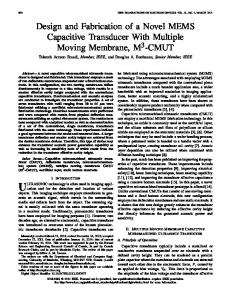
at microwave frequencies [2-4]. Due to the articulate geometry of such switches, a full wave analysis is needed to characterize those switches. The result of the full wave analysis will provide scattering parameters for different switch geometries, which will allow to construct an equivalent lumped circuit model for different geometries. Based on this data base, the equivalent lumped circuit model of the switch is determined. The values of the circuit elements are related to the physical dimensions of the switch as final result. THE ELECTROMAGNETIC MODEL In this paper, we will focus on the shunt capacitive MEMS switch, which consists of a thin metal membrane bridge suspended over the center conductor of a coplanar waveguide (CPW) and fixed on the ground conductor of the CPW, as schematically shown in Fig. 1(a). The parameters L and H indicate the length and the height of the membrane bridge in this figure. The full wave electromagnetic simulation of the switch is done using Ansoft High Frequency Structure Simulator (HFSS). In the simulation a box size 1200 x 600 x 600 µm is used and boundary radiation conditions are imposed on the
six sides of the box. After the full wave analysis is performed, S-parameters are extracted in the frequency range going from 1 GHz to 60 GHz for different heights of the switch. The substrate is assumed to be lossless with relative dielectric constant of 9.8 (correspondent to Alumina). The thickness of the substrate is 600µm and the CPW conductors and MEMS switch are treated as perfect conductors. The central conductor of the CPW is assumed to be coated with silicon nitrate (Si3N 4) having relative dielectric constant of 7 and thickness of 0.1 µm. Figure 1(b) presents the first order equivalent circuit model obtained for the capacitive MEMS switch.
The parameters of the model are optimized to fit the S-parameter obtained from the full wave electromagnetic simulation. Figure 2 shows the EM simulated and circuit model S-parameters of a 300 µm by 200 µm membrane suspended 5 µm over a CPW transmission line having a center conductor width of 100µm and a gap of 50µm. Since the capacitance is very small and it dominates the shunt impedance, it is very difficult to determine the resistance and inductance associated with the model in this state (off-state). The capacitance in the circuit model for this state is 0.0493pF. 0
Si3 N4
S-Parameters (dB)
L MEMS bridge
H
Substrate
-10 -20 -30
S11(HFSS) S21(HFSS) S11(Model) S21(Model)
-40
a) -50 10
CPW
Trans. line
20
30
40
50
60
Frequency (GHz)
Trans. line L C R
b) Fig. 1 (a) Cross section of the capacitive MEMS switch over CPW line. (b) Equivalent circuit model of the capacitive MEMS switch
Fig. 2 S-parameters of the EM simulated and circuit modeled for 300µm long, 5µm gap switch off-state
When the switch is in the on-state, similar procedure is used and S-parameters obtained from the full wave analysis are compared with those obtained using our model in Fig. 3.
5
S-Parameters (dB)
0 -5
S11(HFSS) S21(HFSS) S11(Model) S21(Model)
-10 -15 -20 -25 -30 -35
0
10
20
30
40
50
60
Frequency (GHz)
Fig. 3 S-parameters of the EM simulated and circuit modeled for 300µm long 5µm height switch in the onstate
In both cases excellent agreement is obtained between the simulated data and our lumped circuit model. More results for the lumped circuit parameters for different switch dimensions and states are reported in Table 1
switch capacitance in the off-state versus the switch height. The height of the switch is varied between 3.0µm and 5.0µm and results of the fitting are reported in Fig.4. Also Fig. 4 shows the computed capacitance corresponding to two overlapping parallel plates. It is clear from the comparison that the overlap capacitance has lower value compared to the one predicted by our model and by the full wave analysis due to the fringing field effects at the switch edges. From the curve in Fig. 4, a linear fitting for the switch capacitance versus the inverse of the switch height is obtained, as reported in Eq.(1) C( pF ) = 0.00799 +
Length (µm)
L (pH)
C (pF)
R (Ω)
0.08
ON
300
0.834
2.91
0.589
0.07
ON
400
1.065
2.95
0.454
OFF
300
NA
0.0493
NA
Table 1 Circuit model parameters of the MEMS switch
By repeating this process for different switch height a full set of capacitance of the bridge is obtained and used to extract the parametric scalable model as explained in the next section. PARAMETRIC SCALABLE MODEL From the result of the full wave analysis, we observe as in the off-state condition of the switch the capacitance is dominating the total value of the impedance of the circuit in Fig. 1(b). For the parametric fitting we show the dependence of the
Capacitance (pF)
Switch state
0.20695 H (µm)
(1)
Circuit model Overlapping
0.06
0.05
0.04
0.03 0.18
0.2
0.22
0.24
0.26
0.28
0.3
0.32
0.34
1/H(µm-1)
Fig.4 Capacitance of the circuit model as function of the inverse of the height of the switch
In Fig.5 the capacitance of the switch in the OFF state condition is reported for different width of the switch membrane. In this case the membrane is suspended at 3.5µm from the CPW central conductor. The CPW is printed on silicon
substrate (εr=11.7). The CPW line has a center conductor of 120µm and a gap of 80µm
Capacitance (pF)
0.12
Capacitance (pF) Fitting (pF)
0.1
0.08
0.06
0.04 50
100
150
200
Width (µm)
Fig.5 Capacitance of the circuit model as function of the membrane width for fixed height of the switch
A linear fitting for the switch capacitance versus the width of the switch membrane is obtained, as reported in Eq.(2) C(pF)=0.0107+5.997•10-4 W (µm)
(2)
To validate our model a comparison between measured data from C. L. Goldsmith et. al. [3] and predicted one's from our model is reported in Fig. 6 S-Parameters (dB)
0 -10 -20 -30
S11(Model) S21(Model) S11(Measurement) S21(Measurement)
-40 -50
0
5
10
15
20
25
30
35
Frequency (GHz)
Fig.6 Comparison between measured and simulated results
40
CONCLUSIONS A parametric model based on full wave analysis capable of predicting the performance in the offstate of MEMS capacitive switches has been developed in this work. The good agreement between computed and measured data confirms the validity of the model. As a final result, a lumped elements circuit can easily be implemented into the existing microwave CAD. AKNOLEDGMENTS This work is partially supported by Raytheon Corporation under the MICRO program (Grant 99-031) REFERENCES [1] F. D. Flaviis and R. Coccioli, “Combined mechanical and electrical analysis of microelectromechanical switch for RF applications,” presented at European Microwave Conference EUMC 1999, Munich, Germany, 1999. [2] C. Goldsmith, T. H. Lin, B. Powers, W. R. Wu, and B. Norvell, “Micromechanical membrane switches for microwave applications,” presented at IEEE MTT-S Digest, Orlando Florida May 16, 1995. [3] C. L. Goldsmith, Z. Yao, S. Eshelman, and D. Denniston, “Performance of Low-Loss RF MEMS Capacitive Switches,” IEEE Microwave and Guided Wave Letters, vol. 8, pp. 269-271, 1998. [4] J. B. Muldavin and G. M. Rebeiz, “30 GHz Tuned Mems Switched,” IEEE MTTSymposium, 1998.