IEEE TRANSACTIONS ON COMPUTER-AIDED DESIGN OF INTEGRATED CIRCUITS AND SYSTEMS, VOL. 29, NO. 6, JUNE 2010
897
A Reconfigurable Source-Synchronous On-Chip Network for GALS Many-Core Platforms Anh T. Tran, Dean N. Truong, and Bevan M. Baas
Abstract—This paper presents a GALS-compatible circuitswitched on-chip network that is well suited for use in many-core platforms targeting streaming DSP and embedded applications which typically have a high degree of task-level parallelism among computational kernels. Inter-processor communication is achieved through a simple yet effective reconfigurable sourcesynchronous network. Interconnect paths between processors can sustain a peak throughput of one word per cycle. A theoretical model is developed for analyzing the performance of the network. A 65 nm CMOS GALS chip utilizing this network was fabricated which contains 164 programmable processors, three accelerators and three shared memory modules. For evaluating the efficiency of this platform, a complete 802.11a WLAN baseband receiver was implemented. It has a real-time throughput of 54 Mbps with all processors running at 594 MHz and 0.95 V, and consumes an average of 174.8 mW with 12.2 mW (or 7.0%) dissipated by its interconnect links and switches. With the chip’s dual supply voltages set at 0.95 V and 0.75 V, and individual processors’ oscillators operating at workload-based optimal frequencies, the receiver consumes 123.2 mW, which is a 29.5% reduction in power. Measured power consumption values from the chip are within 2–5% of the estimated values. Index Terms—GALS, source-synchronous, interconnect, 2-D mesh, reconfigurable, programmable, DSP, embedded, network on-chip, many-core chip.
I. I NTRODUCTION Fabrication costs for state-of-the-art chips now exceed several million dollars, and design costs associated with everchanging standards and end user requirements are also extremely expensive. In this context, programmable and/or reconfigurable platforms that are not fixed to a single application or a small class of applications become increasingly attractive. The power wall limits the performance improvement of conventional designs exploiting instruction-level parallelism that rely mainly on increasing clock rate with deeper pipelines. Many new techniques and architectures have been proposed in the literature; and multiple-core designs are the most promising approaches among them [1], [2]. Recently, a large number of multi-core designs were found in both industry and academia [3]–[6]. Also, reconfigurable and programmable many-core designs for DSP and embedded applications are becoming popular research topics [7]–[9]. Transistor density and integration continue to scale with Moore’s Law, and for practical digital designs, clock distribution becomes a critical part of the design process for any high performance chip [10]. Designing a global clock tree for a large chip becomes very complicated and it can consume a Copyright (c) 2010 IEEE. Personal use of this material is permitted. However, permission to use this material for any other purposes must be obtained from the IEEE by sending an email to
[email protected].
significant portion of the power budget, which can be up to 40% of the whole chip’s power [11]. One effective method to address this issue is through the use of globally-asynchronous locally-synchronous (GALS) architectures where the chip is partitioned into multiple independent frequency domains. Each domain is clocked synchronously while inter-domain communication is achieved through specific interconnect techniques and circuits [12]. Due to its flexible portability and “transparent” features regardless of the differences among computational cores, GALS interconnect architecture becomes a top candidate for multi- and many-core chips that wish to do away with complex global clock distribution networks. In addition, GALS allows the possibility of fine-grained power reduction through frequency and voltage scaling [13]. The methodology of inter-domain communication is a crucial design point for GALS architectures. One approach is the purely asynchronous clockless handshaking, that uses multiple phases (normally two or four phases) of exchanging control signals (request and ack) for transferring data words across clock domains [14], [15]. Unfortunately, these asynchronous handshaking techniques are complex and use unconventional circuits (such as the Muller C-element [16]) typically unavailable in generic standard cell libraries. Besides that, because the arrival times of events are arbitrary without a reference timing signal, their activities are difficult to verify in traditional digital CAD design flows. The so-called delay-insensitive interconnection method extends clockless handshaking techniques by using coding techniques such as dual-rail or 1-of-4 to avoid the requirement of delay matching between data bits and control signals [17]. These circuits also require specific cells that do not exist in common ASIC design libraries. Quinton et al. implemented a delay-insensitive asynchronous interconnect network using only digital standard cells; however, the final circuit has large area and energy costs [18]. Another asynchronous interconnect technique uses a pausible or stretchable clock where the rising edge of the receiving clock is paused following the requirements of the control signals from the sender. This makes the synchronizer at the receiver wait until the data signals stabilize before sampling [19], [20]. The receiving clock is artificial meaning its period can vary cycle by cycle; so it is not particularly suitable for processing elements with synchronous clocking that need a stable signal clock in a long enough time. Besides that, this technique is difficult to manage when applied to a multiport design due to the arbitrary and unpredictable arrival times of multiple input signals. An alternative for transferring data across clock domains
IEEE TRANSACTIONS ON COMPUTER-AIDED DESIGN OF INTEGRATED CIRCUITS AND SYSTEMS, VOL. 29, NO. 6, JUNE 2010
is the source-synchronous communication technique that was originally proposed for off-chip interconnects. In this approach, the source clock signal is sent along with the data to the destination. At the destination, the source clock is used to sample and write the input data into a FIFO queue while the destination clock is used to read the data from the queue for processing. This method achieves high efficiency by obtaining an ideal throughput of one data word per source clock cycle with a very simple design that is also similar to the synchronous design methodology; hence it is easily compatible with common standard cell design flows [21]–[24]. In this paper, we present the design of a GALS manycore computational platform utilizing a source-synchronous communication architecture. In order to evaluate the efficiency of this platform and its interconnection network, we mapped a complete 802.11a WLAN baseband receiver on this platform. Actual chip measurement results are reported, analyzed, and compared against simulation. The outline of the paper is organized as follows. Section II explains our motivation for designing a GALS many-core heterogeneous platform for DSP applications. Design of a reconfigurable source-synchronous interconnect network is described in Section III. In this section, we also derive a theoretical model for analyzing the throughput and latency of interconnects established from the network. The design of our many-core DSP platform utilizing this network architecture is shown in Section IV. This section also shows the implementation and measurement results of the test chip. Mapping, analyzing and measuring the performance and power consumption of an 802.11a baseband receiver on this platform as a case study is discussed in Section V. Finally, Section VI concludes the paper. II. M OTIVATION F OR A GALS M ANY-C ORE P LATFORM A. High Performance with Many-Core Design Pollack’s Rule states that performance increase of an architecture is roughly proportional to the square root of its complexity [13]. This rule implies that if we apply sophisticated techniques to a single processor and double its logic area, we speedup its performance by only around 40%. On the other hand, with the same area increase, a dual-core design using two identical cores could achieve a 2x improvement assuming that applications are 100% parallelizable. With the same argument, a design with many small cores should have more performance than one with few large cores for the same die area. However, performance increase is heavily hindered by Amdahl’s Law, which implies that this speedup is strictly dependent on the application’s inherent parallelism: Speedup ≈
1 (1 − Parallel%) +
1 N
· Parallel%
(1)
where N is the number of cores. Fortunately, for most applications in the DSP and embedded domain, a high degree of task-level parallelism can be easily exposed [7] through their task-graph representatives such as a complete 802.11a baseband receiver shown in Fig. 1. By partitioning the natural task-graph description of a DSP application, where each task can easily fit into one or few small processors,
Signal Energy Comput. from ADC
Frame Detection
Data Dist.
Timing Synch.
898
CFO Estimation
Acc. CFO Vector
Post Timing Synch.
CFO Compen.
Guard Removal
64-pt FFT
Subcarrier Reordering
Autocorrelation
Depuncturing
Deinterleav. Step 2
Viterbi Decoder
Deinterleav. Step 1
Constell. Demapping
SIGNAL decoding
Channel Equalizer
Pad Removal
Channel Estimation
to MAC layer
Descrambl.
Fig. 1. Task-interconnect graph of an 802.11a WLAN baseband receiver. The dark lines represent critical data interconnects.
Accelerator 1
Accelerator 2
Shared Memory
Accelerator 3
Fig. 2. Illustration of a GALS many-core heterogeneous system consisting of many small identical processors, dedicated-purpose accelerators and shared memory modules running at different frequencies and voltages or fully turned off.
the complete application will run much more efficiently. This is due to the elimination of unnecessary memory fetching and complex pipeline overheads. In addition, the tasks themselves run in tandem like coarse pipeline stages. B. Advantages of the GALS Clocking Style Since each core operates in its own frequency domain, we are able to reduce the power dissipation, increase energy efficiency and compensate for some circuit variations on a fine-grained level as illustrated in Fig. 2: • GALS clocking design with a simple local ring oscillator for each core eliminates the need for complex and power hungry global clock trees. • Unused cores can be effectively disconnected by power gating, and thus reducing leakage. • When workloads distributed for cores are not identical, we can allocate different clock frequencies and supply voltages for these cores either statically or dynamically. This allows the total system to consume a lower power than if all active cores had been operating at a single frequency and supply voltage [25]. • We can reduce more power by architecture-driven methods such as parallelizing or pipelining a serial algorithm over multiple cores [26]. • We can also spread computationally intensive workloads around the chip to eliminate hot spots and balance temperature.
IEEE TRANSACTIONS ON COMPUTER-AIDED DESIGN OF INTEGRATED CIRCUITS AND SYSTEMS, VOL. 29, NO. 6, JUNE 2010
899
North wire
Co re
North Switch B
...
Switch A
Core
West
Osc
East
driver
Processor
Switch
East
West
FIFO
South
(a) South
Fig. 3. The many-core platform from Fig. 2 with switches inside each processor that can establish interconnects among processors in a reconfigurable circuit-switched scheme.
(b)
Fig. 4. (a) A unidirectional link between two nearest-neighbor switches includes wires connected in parallel. Each wire is driven by a driver consisting of cascaded inverters. (b) A simple switch architecture consisting of only five 4-input multiplexers. Link
GALS design flexibility supports remapping or adjusting frequencies of processors in an application that allows it to continue working well even under the impact of variations. From these advantages in both performance and power consumption, many-core GALS style is highly desirable for designing programmable/reconfigurable DSP computational platforms. However, the challenge now is how to design a low area and power cost interconnect network that is able to offer low latency and high communication bandwidth for these GALS many-core platforms. Next section describes our proposed reconfigurable network utilizing a novel sourcesynchronous clocking scheme for tackling this challenge. •
III. D ESIGN AND E VALUATION OF A R ECONFIGURABLE GALS C OMPATIBLE S OURCE -S YNCHRONOUS O N -C HIP N ETWORK The static characteristic of interconnects in the task-graphs of DSP and embedded applications motivates us to build a reconfigurable circuit-switched network for our many-core platform. The network is configured before run-time to establish static interconnects between any two processors described by the graph. Due to its advantages compared to clockless handshaking techniques as explained in Section I, the sourcesynchronous communication technique is utilized in our interconnect networks for transferring data across clock domains in our GALS array of processors. This section presents the design of our reconfigurable interconnection network; and also describes how inter-processor interconnects are configured. Evaluation of throughput and latency of these interconnects are given through formulations developed from timing constraints combined with delay values obtained from SPICE models. A. Architecture of Reconfigurable Interconnection Network Figure 3 shows the targeted GALS many-core platform from Fig. 2 but focuses on its interconnect architecture. Processors are interconnected by a static 2-D mesh network of reconfigurable switches. Each switch connects with its nearest neighboring switch by two unidirectional links where each link is composed of metal wires in parallel as depicted in Fig. 4(a); one wire per data bit. Each wire is driven by a cascade of inverters that are appropriately sized. An interconnect path between any two processors is formed from one or many links connecting intermediate switches.
Osc
Osc
Core
Osc
Core
FIFO
Proc. A
Core
FIFO
Proc. B
Switch
FIFO
Proc. C
Path clock data
Osc
Core
valid
FIFO
full
Proc. D
Fig. 5. Illustration of a long-distance interconnect path between two processors directly through intermediate switches. On this interconnect, data are sent with the clock from the source processor to the destination processor.
We will investigate the throughput and latency of interconnects that are configured from switches with the architecture consisting of only 4-input multiplexers as shown in Fig. 4(b). The switch has five ports: the Core port which is connected to its local core, and the North, South, West, and East ports which are connected to its four nearest neighbor switches. As shown in the figure, an input from the West port can be configured to go out to any port among the Core, North, South, East ports and vice versa. For simplicity, we only shows its full connections to and from the West port; all the other ports are connected in a similar fashion. Figure 5 illustrates an example of a long-distance interconnection from Proc. A to Proc. D passing through two intermediate processors B and C. This interconnection is established by configuring the multiplexers in the switches of these four processors. The configuration is done pre-runtime which fixes this communication path; thus, this static circuitswitched interconnect is guaranteed to be independent and never shared. So long as the destination processor’s FIFO is not full, a very high throughput of one data word per cycle can be sustained. This compares favorably to a packet-switched network whose runtime network congestion can significantly degrade communication performance [23], [27]. On this interconnect path, the source processor (Proc. A) sends its data along with its clock to the destination. The destination processor (Proc. D) uses a dual-clock FIFO to buffer the received data before processing. Its FIFO’s write port is clocked by the source clock of Proc. A, while its read port is clocked by its own oscillator, and thus supports GALS
IEEE TRANSACTIONS ON COMPUTER-AIDED DESIGN OF INTEGRATED CIRCUITS AND SYSTEMS, VOL. 29, NO. 6, JUNE 2010
Proc. B
Proc. A
Proc. C
Proc. D
clock buffer dest. clock
source clock
TABLE I D IMENSIONS OF INTERCONNECT WIRES AT THE INTERMEDIATE LAYER BASED ON ITRS [32] AND WITH RESISTANCE AND CAPACITANCE CALCULATED BY USING PTM ONLINE TOOL [34]
dest. data
source data
FIFO
N bits
N wires input dual-clock FIFO
output register switch
Fig. 6.
900
A simpified view of the interconnect path shown in Fig. 5. s
w
Upper Layer
Cg Cc
Cc
25x
Rw/3
A 2Cg/6
Lower Layer
B
Fig. 7. A side view of three metal layers where the interconnect wires are routed on the middle layer. Each wire has ground capacitances with upper and lower metal layers and coupling capacitances from adjacent intra-layer wires.
5x
25x
Rw/3
2Cg/6 C
5x
25x
Rw/3
Rw/3
Rw/3
CL
Cc/6
2Cg/6
Cc/3
Rw/3
2Cg/3
CL
Cc/6
2Cg/6
CL ...
In order to characterize performance of interconnects we firstly consider wires that are connected between two adjacent switches. These wires are routed on intermediate layers where the lower layers (metal 1 or 2) are used for intra-cell or inter-cell layouts and the upper layers are reserved for power distribution and other global signals. In this work, we assume all interconnect wires are on the same layer and have the same length when connecting two adjacent switches. An interconnect wire in the intermediate layer incurs both ground and coupling capacitances as depicted in Fig. 7. These capacitance values depend on the metal wire dimensions
Cc/3
...
C. Link and Device Delays
2Cg/6
2Cg/3
Cc/3
...
Evaluation of the characteristics of these reconfigurable interconnects are based on the delay values simulated by HSPICE. Simulation setups were performed through the use of CMOS technology cards given by the Predictable Technology Model (PTM) [31]. For analyzing the effect of technology scaling on interconnect performance, we ran simulations on five technology nodes: 90 nm, 65 nm, 45 nm, 32 nm and 22 nm. The wire dimensions used for simulation were derived from the reports of the International Technology Roadmap for Semiconductors (ITRS) [32].
Rw/3
2Cg/3 ...
B. Approach Methodology
Cc/3
22 50 60 98 89 1.7 489 2018.4 7.6 17.7
Rw/3
2Cg/3
2Cg/3
Cc/6
2Cg/6
communication. Storage elements inside the FIFO can be an SRAM array [28], [29] or a set of flip-flop registers [23], [30]. Data sent on this interconnect path will pass through four multiplexers (of four corresponding switches) and three switch-to-switch links as shown in Fig. 6. These switches are not only responsible for routing data on the links but also act as repeaters along the long path when combined with wire drivers.
Rw/3
2Cg/3
Cc/6
32 72 81 135 121 1.9 711 1481.1 12.9 27.2
...
5x
h
45 102 116 183 162 2.1 1000 1084.7 21.3 39.8
...
t Cg
65 147 158 264 234 2.4 1444 753.8 35.0 65.9
...
...
90 207 222 351 309 2.7 2000 556.9 57.7 96.6
...
...
Technology (nm) width w (nm) space s (nm) thickness t (nm) height h (nm) κILD length l (µm) Rw (Ω) Cg (fF) Cc (fF)
Fig. 8. Circuit model used to simulate the worst case and best case interswitch link delay considering the crosstalk effect between adjacent wires. Wires are simulated using a Π3 lumped RC model.
(space s, width w, thickness t, height h, length l) and the interlayer dielectric κILD that can be calculated from formulations proposed by Wong et al. [33]. These formulations are also used by PTM on their online interconnect tool [34]. Table I shows the wire dimensions and intra-layer dielectric based on ITRS, that was used in a paper by Im et al. [35], and its calculated resistances and capacitances over many technology nodes from 90 nm down to 22 nm. The wire length is 2 mm at 90 nm technology and is scaled correspondingly to each technology node. Notice that the wire length connecting two adjacent switches approximates the length (or width) of a processor in the platform as seen in Fig. 5. With these simple processors, a 20 mm x 20 mm die (400 mm2 ) would contain 100 processors at 90 nm and up to 1672 processors at 22 nm. For estimates of the switch-to-switch link delay while considering the effect of crosstalk noise due to coupling capacitances, we used the Π3 lumped RC model for setup wires in HSPICE. Higher degree models such as Π5 or so on can make the simulation results more accurate but also slows down the simulation time. The Π3 model was proven to have an error of less than 3% compared with the accurate value of a distributed RC model [16]. Fig. 8 shows our circuit setup for simulation of wires in an inter-switch link including the coupled capacitances among them1 . In this setup, load capacitance C L is equivalent to the input gate capacitance of 1 For more accuracy, we can consider the multi-coupled case that takes into account capacitances coupled with far wires rather than only adjacent wires [36]. However, the coupled capacitances from far wires are very small in compared with those from adjacent wires, so their impacts are negligible [37].
IEEE TRANSACTIONS ON COMPUTER-AIDED DESIGN OF INTEGRATED CIRCUITS AND SYSTEMS, VOL. 29, NO. 6, JUNE 2010
901
Timing uncertainty clock @ source processor data bit @ source processor
Dpath,max + Dclkbuff,FIFO Dpath,min + Dclkbuff,FIFO
clock @ destination input FIFO
Dclkbuff,flip-flop + tclk-q + Dpath,max Dclkbuff,flip-flop + tclk-q + Dpath,min
data bit @ destination input FIFO clock @ destination input FIFO after inserted a delay
Dlnsert safe rising edges
Fig. 9.
Timing waveforms of clock and data signals from the source processor to the destination FIFO
TABLE II D ELAY VALUES SIMULATED USING PTM TECHNOLOGY CARDS Technology (nm) Supply Voltage Vdd (V) Threshold Voltage Vth (V) Dlink,max (ps) Dlink,min (ps) Dclkbu f f, f lip f lop (ps) Dclkbu f f,FIFO (ps) Dmux (ps) t setup (ps) thold (ps) tclk−q (ps)
90 1.20 0.30 271.8 131.4 37.0 93.2 48.1 25.2 -18.9 104.5
65 1.10 0.28 223.8 102.3 27.9 69.8 37.7 20.1 -15.1 83.8
45 1.00 0.25 142.9 60.5 13.4 25.9 16.8 11.0 -5.2 38.6
32 0.90 0.23 123.1 47.6 9.4 18.2 13.2 9.9 -3.9 23.2
22 0.80 0.20 104.7 38.5 7.2 14.2 11.3 7.0 -3.1 22.1
a 4-input multiplexer. The delay of a circuit is measured from when its input point reaches 0.5Vdd until the output point also reaches 0.5Vdd . Due to crosstalk, depending on the data patterns sent on the wires, three cases of delay are experienced. The nominal delay happens when the signal on a wire goes high while both its neighboring wires do not change. The best case delay Dlink,min occurs when the signal on a wire moves in the same direction with its two neighbors; and the worst case delay Dlink,max occurs when the signal on that wire switches in the opposite direction with its neighbors. The simulated delay values with respect to each CMOS technology node are given in Table. II. This table also lists the values of Vdd and threshold voltage Vth used in the simulations. Values of Vdd at each technology node are predicted by Zhao and Cao [31], and those of Vth are assumed to be 1 4 Vdd [38]. In this table, we also include the delays of clock buffers when driving a flip-flop stage (Dclkbu f f, f lip f lop ), a FIFO (Dclkbu f f,FIFO ) and the delay of a 4-input multiplexer (Dmux ). We simulated a static positive D flip-flop using minimumsize transistors and its setup time t setup , hold time thold and propagation delay tclk−q are also shown in the table. A minor note is that the flip-flop has negative hold time, which means that it can correctly latch the current data value even when the rising clock edge arrives just after a new transition of data bits. D. Interconnect Throughput Evaluation For an interconnect path between two processors in a distance of n link segments, this path will travel through n + 1 switches including those of the source and destination
inserted delay dest. clock
source clock
dest. data
source data
FIFO
Fig. 10. Interconnect circuit path with a delay line inserted in the clock signal path before the destination FIFO to shift the rising clock edge to a stable data window
processors (as depicted in Fig. 6) that passes through n + 1 multiplexers and n inter-switch links. Therefore, its minimum (best case) and maximum (worst case) delays are: D path,min = n · Dlink,min + (n + 1)Dmux
(2)
D path,max = n · Dlink,max + (n + 1)Dmux
(3)
and Figure 9 shows timing waveforms of the clock and corresponding data sent from a source to its destination. Data bits are sent at the rising edge of the source clock and each bit is only valid in one cycle. Both clock and data bits travel in the same manner on the configured interconnect path and therefore have the same timing uncertainty with a small delay difference: the clock signal has to pass through a clock buffer before driving the destination FIFO while the data signal has a clock buffer delay at the output register of the source processor and a tclk−q delay before traveling on the interconnect path. As seen in the figure, due to the timing uncertainty of both clock and data signals, metastability can occur at the input of destination FIFO when they transit at almost same time. For safety, we have purposely inserted a delay line on the clock signal before it drives the destination FIFO (as shown in Fig. 10), effectively moving the rising clock edge into the stable window between two edges of the data bits as depicted in the last waveform of Fig. 9. The value of the inserted delay Dinsert must satisfy the setup time constraint: Dinsert + nDlink,min + (n + 1)Dmux + Dclkbu f f,FIFO > Dclkbu f f, f lip f lop + tclk−q + nDlink,max + (n + 1)Dmux + t setup or Dinsert > n(Dlink,max − Dlink,min ) + Dclkbu f f, f lip f lop − Dclkbu f f,FIFO + t setup + tclk−q (4) Given a delay value Dinsert satisfying the above condition, the period of source clock used on the interconnect also has
IEEE TRANSACTIONS ON COMPUTER-AIDED DESIGN OF INTEGRATED CIRCUITS AND SYSTEMS, VOL. 29, NO. 6, JUNE 2010
8
5
9 Max Absolute Latency (ns)
6
10 @ 90 nm @ 65 nm @ 45 nm @ 32 nm @ 22 nm
4 3 2
8 7 6
@ 90 nm @ 65 nm @ 45 nm @ 32 nm @ 22 nm
5 4 3 2
1
1
0 0 1 2 4 6 8 10 12 14 16 18 20 Interconnect Distance (number of inter−switch links)
0 0 1 2 4 6 8 10 12 14 16 18 20 Interconnect Distance (number of inter−switch links)
Fig. 11. Maximum frequency of the source clock over various interconnection distances and CMOS technology nodes
to meet the hold time constraint: Dinsert + Dclkbu f f,FIFO + nDlink,max + (n + 1)Dmux + thold < Dclkbu f f, f lip f lop + tclk−q + nDlink,min + (n + 1)Dmux + T clk and therefore, T clk > n(Dlink,max − Dlink,min ) + Dinsert + Dclkbu f f,FIFO − Dclkbu f f, f lip f lop + thold − tclk−q
(5)
The minimum clock period strongly depends on the timing uncertainty (Dlink,max − Dlink,min ) and linearly increases with the interconnect distance n. The maximum frequency (corresponding to the minimum period) of source clock used for transferring data on an interconnect path corresponding to a distance is given in Fig. 11. When connecting two nearest neighboring processors, the interconnect can run at up to 3.5 GHz at 90 nm and up to 7.3 GHz at 22 nm. The maximum frequency is inversely proportional to n that reduces when interconnect distance increases. E. Interconnect Latency Latency of an interconnect path is defined as the time at which a data word is sent by the source processor until it is written to the input FIFO of the destination processor. The data travels along the path, and then registered at the destination FIFO. This path includes both delays by the inserted delay line and clock buffer on the clock signal and also a flip-flop propagation delay tclk−q . Therefore, the maximum latency of an interconnect path with distance of n inter-switch links is given by: Dconnect,max = nDlink,max +(n+1)Dmux +Dinsert +Dclkbu f f,FIFO +tclk−q (6) The maximum absolute latency (in ns) corresponding to distance is plotted in Fig. 12. Consider a nearest neighboring interconnect, which has less than 1 ns latency regardless of the technology used. This means that at 1 GHz the interconnect latency is less than 1 cycle, and at 500 MHz latency is less than a half of cycle. The maximum number of clock cycles that the data will travel on an interconnect distance is given in Fig. 13. This maximum clock cycle latency is equal to the maximum latency (in ns) multiplied by the maximum clock frequency (in GHz) at that distance. Interestingly, the latency cycles even decreases
Fig. 12.
Maximum interconnect latency (in ns) over various distances Max Latency (cycles) at the Max Freq.
Max Frequency (GHz)
7
902
3
2.5
@ 90 nm @ 65 nm @ 45 nm @ 32 nm @ 22 nm
2
1.5
1 0 1 2 4 6 8 10 12 14 16 18 20 Interconnect Distance (number of inter−switch links)
Fig. 13. Maximum communication latency in term of cycles at the maximum clock frequency over interconnect distances
when distance increases. This happens because the clock period is larger for longer distances. In all cases, the latency is less than 2.5 cycles at 90 nm and less than 1.7 cycles at 22 nm regardless of distance. These latencies are very low when compared with dynamic packet-switched networks whose latency (in cycles) is proportional to the distance, which can be very high if routers are pipelined into many stages. F. Discussion on Interconnection Network Architectures The pipelined architecture of routers in a packet-switched network can allow obtaining good throughput but sacrificing the latency in terms of numbers of delay cycles. The situation would be much worse in the presence of network congestion [27]. Moreover, supporting GALS clocking scheme is much expensive and complicated in a packet-switched network where each router runs on its own clock domain [39]. Our interconnects can guarantee an ideal throughput of one data word per cycle because no network contention occurs, while also achieving very low latency of only a few cycles. Furthermore, our interconnect architecture well supports GALS scheme while does not require complicated control circuits and buffers at switches along the interconnect path; therefore, it is also highly efficient in terms of area and power consumption. The network circuit occupies only 7% of each programmable processor’s area 2 and only consumes 10% of 2 Note that this area is sum of two static networks, so each network occupies only 3.5% of the processor’s area.
IEEE TRANSACTIONS ON COMPUTER-AIDED DESIGN OF INTEGRATED CIRCUITS AND SYSTEMS, VOL. 29, NO. 6, JUNE 2010
serial configuration bit-stream input mux select
903
test out
Configuration and Test Logic
output mux select
output data, valid and clock
input data, valid and clock input request
output request
Supply Voltages
Controller
Osc.
CORE Datapath
Switch
Fig. 15. Simplified block diagram of processors or accelerators in the proposed heterogeneous system. Processor tiles are virtually identical, differing only in their computational core. Motion Estimation
to analog pads
Viterbi Decoder FFT 16 KB Shared Memories
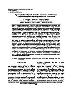
Fig. 14. Block diagram of the 167-processor heterogeneous computational platform [40]
the total power while mapping a complex application as shown in Section V. These advantages along with the deterministic characteristic of interconnects in DSP applications we are targeting support the idea of building a reconfigurable circuitswitched network for our platform. However, these advantages come with a cost of sacrificing the flexibility and interconnect capacity. Programmer (under the help of automatic tools) has to setup all interconnects before an application can run. In addition, the number of interconnect links are limited and interconnects after configured are not shared; therefore, for some complex applications, it is difficult for setting up all connects or even there are not enough links required. For increasing the interconnect capacity, the platform is equiped with two static configurable networks as will be described in Section IV-B. IV. A N E XAMPLE H ETEROGENEOUS GALS M ANY- CORE P LATFORM The top level block diagram of our 167-processor computational platform is shown in Fig. 14. The platform consists of 164 small programmable processors, three accelerators (FFT, Viterbi decoder and Motion Estimation), and three 16 KB shared memory modules [40]. Placement of the three accelerators and the three shared memories at the bottom of the array was chosen only to simplify the routing of global configuration signal wires and to simplify mapping of applications onto the large central homogeneous array (as opposed to breaking up the array by placing accelerators or memories in the middle). Because of the array nature of the platform, the local oscillator, voltage switching, configuration and communication circuits are reused throughout the platform. These common components are designed as a generic “wrapper” which could then be reused to make any computational core compatible with the GALS array, and thus facilitates easy design enhancements. The difference between the programmable processors and the accelerators is mainly in their computational datapaths as illustrated in Fig. 15. The programmable processors have an in-order single-issue 16-bit fixed point datapath, with a
128×16-bit DMEM, a 128×35-bit IMEM, two 64×16-bit dualclock FIFOs, and they can execute 60 basic ALU, MAC, and branch type instructions. A. Per-Processor Clock Frequency and Supply Voltage Configuration All processors, accelerators and memory modules operate at their own fully-independent clock frequency that is generated by a local clock oscillator and is able to arbitrarily halt, restart, and change frequency. During runtime, processors fully halt their clock oscillator six cycles after there is no work to do (for finishing all instructions already in the pipeline), and they restart immediately once work becomes available. Each ring oscillator supports frequencies between 4.55 MHz and 1.71 GHz with a resolution of less than 1 MHz [40]. Off-chip testing is used to determine the valid operational frequency settings for the ring oscillator of each processor, which takes into account process variations. The platform is powered by two independent power grids which will in general, have different supply voltages. Processors may also be completely disconnected from either power grid when they are unused. The benefits of having more than two supply voltages are small when compared to the increased area and complexity of the controller needed to effectively handle voltage switching [41]. Using two supply voltages for power management was also employed in the ALPIN test chip [42]. Although the processors have hardware to support dynamic voltage and frequency scaling (DVFS) through software or a local DVFS controller [40], [43], dynamic analyses are much more complex and do not demonstrate the pure frequency and voltage gains as clearly as with static assignments. In addition, due to its control overhead, an application running in a DFVS mode may actually dissipate more power if the workload is predictable pre-runtime and is relatively static. Data and analysis throughout this work utilizes clock frequencies and supply voltages that are kept constant throughout workload processing. Static configuration is intentionally set by the programmer for a specific application to optimize its performance and power consumption. This method is especially useful for applications that have a relatively static load behavior at runtime. The frequency and supply voltage of each processor are controlled by its VFC that is depicted in Fig. 16.
IEEE TRANSACTIONS ON COMPUTER-AIDED DESIGN OF INTEGRATED CIRCUITS AND SYSTEMS, VOL. 29, NO. 6, JUNE 2010
•
65 nm STMicroelectronics
904
410 ȝm
VddHigh VddLow VddOsc VddAlwaysOn
410 ȝm
control_high control_low control_freq
config signals from core
5.939 mm
Volt. & Freq. Controller
VddCore
Osc Switch
1.19 GHz, 1.3 V GndOsc GndCom
66 MHz, 0.675 V Fig. 16.
Mot. Est. Mem
The Voltage and Frequency Controller (VFC) architecture
Mem Mem Vit
FFT
1.095 GHz, 1.3V 5.516 mm Osc
Fig. 18.
Osc
Core
Core FIFO
FIFO
Switch
Processor
Switch
Processor
Fig. 17. Each processor tile contains two switches for the two parallel but separate networks
The VFC and communication circuits operate on their own supply voltage that is shared among all processors in the platform to guarantee the same voltage level for all interconnect links, thus avoiding the use of level shifters between switches.
B. Source-Synchronous Interconnection Network All processors in the platform are interconnected using a reconfigurable source-synchronous interconnect network as described in Section III. To increase the interconnect capacity, each processor has two switches as depicted in Fig. 17 and, correspondingly, has two dual-clock FIFOs – each per switch (on the output of its Core port). These switches connect to their nearest neighboring switches to form two separate 2-D mesh networks; simplifying the mapping job for programmers. Furthermore, two networks naturally support tasks that need two input channels3 . A reconfigurable delay line is inserted on the clock signal before each FIFO to adjust its delay value for matching with its corresponding data. The reconfigurable delay line is a simple circuit including many delay elements and configured by multiplexers for setting a delay value. The delay value is chosen corresponding to the interconnect distance for satisfying constraint (4). For interconnects of a mapped application, their distances are known; therefore the corresponding delay values are statically set. Thanks to these static settings, the delay circuits do not cause any glitch on the clock signals at run-time. 3 For
tasks need more than two input channels, it is easy to use some intermediate processors for collecting and converting these inputs into two channels.
Die micrograph of the 167-processor test chip
C. Platform Configuration, Programming and Testability For array configuration (e.g. circuit-switch link configurations, VFC settings, etc.), the compiler, assembler and mapping tools place programs and configurations into a bitstream that is sent over a Serial Peripheral Interface (SPI) into the array as depicted at top of Fig. 14. This technique needs only a few I/O pins for chip configuration. The configuration information and instructions as well as address of each processor are sent into the chip in a serial manner bit by bit along with an off-chip clock. Based on the configuration code, each processor will set its frequency and voltage; and the multiplexers and delay lines of its switches are also configured for establishing communication paths. Our current test chip employs a simple test architecture for functional testing only that determines whether a processor operates correctly. Test outputs of all processors share the same the ”test out” pins as shown at the top of Fig. 14. Therefore, there is only one processor that can be tested at a time, but this can be easily reconfigured by an off-chip test environment with test equipment (e.g. logic analyzer). Test signals include all key internal control and data values. Our current test architecture works well at the processor level that is acceptable for a research chip. High-volume manufacturing would require the addition of special circuits (e.g. scan path) for rapid high-fault-coverage testing [44], [45]. D. Chip Implementation The platform was fabricated in ST Microelectronics 65 nm low-leakage CMOS process using a standard-cell design flow. Its die micrograph is shown in Fig. 18. It has a total of 55 million transistors with an area of 39.4 mm 2 . Each programmable processor occupies 0.17 mm2 , with its communication circuit occupying 7%, including the two switches, wires and buffers. The area of the FFT, motion estimation and Viterbi decoder accelerators is six times, four times and one time, respectively, that of one processor; the memory module is two times the size of one processor. E. Measurements We tested all processors in the platform to measure their maximum operating frequencies. The maximum frequency is
60
1000
50
800
40
600
30
400
20
200
10
0 0.6
0.7
0.8
0.9 1.0 1.1 Supply Voltage (V)
1.2
1.3
0
Fig. 19. Maximum clock frequency and 100%-active power dissipation of one programmable processor over various supply voltages TABLE III AVERAGE POWER CONSUMPTION MEASURED AT 0.95 V AND 594 MH Z Operation of Processor FFT Viterbi FIFO Rd/Wr Switch + Link
100% Active (mW) 17.6 12.7 6.2 1.9 1.1
Stall (mW) 8.7 7.3 4.1 0.7 0.5
Standby (mW) 0.031 0.329 0.153 ∼0 ∼0
obtained once a higher frequency makes outputs of the corresponding processor incorrect. The maximum frequency and power consumption of the programmable processors versus supply voltage is shown in Fig. 19. As shown in the figure, they have a nearly linear and quadratic dependence on the supply voltage, respectively. These important characteristics are used to reduce power consumption of an application by appropriately choosing the clock frequency and supply voltage for each processor as detailed in Section V. At 1.3 V, the programmable processors can operate up to 1.2 GHz. The configurable FFT and Viterbi processors can run up to 866 MHz and 894 MHz respectively. The maximum frequency of each processor should vary under the impact of process and temperature variations. Unfortunately, these measurements have not yet been made. Currently, we can guarantee the correct operation of the mapped application by allowing a frequency margin of 10%-15% of the maximum frequency measured under typical conditions, for each processor. Table III shows the average power dissipation of processor, accelerators and communication circuit at 0.95 V and 594 MHz. This supply voltage and clock frequency is used to evaluate and test the 802.11a baseband receiver application described in the next section. The FFT is configured to perform 64-point transformations, and the Viterbi is configured to decode 1/2-rate convolution codes. The table also shows that during stalls (i.e. non-operation while the clock is active) the processors consume a significant portion, approximately 3555%, of their normal operating power. Leakage power are very small while processors are in the standby mode with the clock halted. Figure 20 plots measured data for maximum allowable source clock frequencies when sending data over a range of interconnect distances at 1.3 V. Interestingly, the measured
Max Clock Frequency (MHz)
1200
Power (mW)
Max Frequency (MHz)
IEEE TRANSACTIONS ON COMPUTER-AIDED DESIGN OF INTEGRATED CIRCUITS AND SYSTEMS, VOL. 29, NO. 6, JUNE 2010
1400 1300 1200 1100 1000 900 800 700 600 500 400 300 200 100 0 0
905
1 2 3 4 5 6 7 8 9 10 11 12 13 Interconnect Distance (number of inter−switch links)
Fig. 20. Measured maximum clock frequencies for interconnect between processors over various interconnect distances at 1.3 V. An Interconnect Distance of one corresponds to adjacent processors.
data has a similar trend as the theoretically developed model depicted in Fig. 11. The differences are due to the assumptions used in the theoretical model versus the real test chip such as wire and device parameters. For the model we assumed wires have the same length and are on the same metal layer with devices modeled from the PTM SPICE cards; while the test chip is built from ST Microelectronics standard cells with wires that are automatically routed along with buffers that are added by Cadence Encounter place and route tool. Besides that, environment parameters, process variation and power supply noise on the real chip add more to these differences. However, the maximum clock frequency strongly depends on the timing uncertainty of clock and data signals that linearly increases following the distance; so both measured and theoretical results come to the same conclusions. Note that, as shown in the figure, because the maximum operating frequency of processors is 1.2 GHz, source-synchronous interconnects with distances of one and two inter-switch links also only run up to 1.2 GHz. The clock frequency of the source processor reduces corresponding to the interconnect distance that affects its computational performance. However, for a good mapping tool or carefully manual mapping, we always want to assign critical processors in an application with high volumes of data communication near together. This guarantees source processors of interconnects still run at high frequency satisfying the application requirement. Another inexpensive solution to maintain a high processor clock frequency while communicating over a long distance is to insert a dedicated “relay” processor into the long path by the fact that the processor has very small area. Furthermore, as shown in Fig. 20, for a communication distance of ten inter-switch links, source processor clocks can operate up to 600 MHz which is sufficient for meeting computational requirements of many DSP applications such as an 25-processor 802.11a WiFi baseband receiver presented in Section V, where the maximum interconnect length is six. Interconnect power corresponding to distance at the same 594 MHz and 0.95 V is given in Fig. 21. These measured power values are nearly linear to distance, which is reasonable due to the fact that interconnect power is proportional to the number of switches and interconnect links that form the
IEEE TRANSACTIONS ON COMPUTER-AIDED DESIGN OF INTEGRATED CIRCUITS AND SYSTEMS, VOL. 29, NO. 6, JUNE 2010
Interconnect Power (mW)
from ADC
14 13 12 11 10 9 8 7 6 5 4 3 2 1 0 0
906
DATA DISTR.
AUTOCORR.
OFFSET VECTOR ACC.
CFO COMPEN.
GUARD REMOV.
ENERGY COMP.
FRAME DET.
CORDIC – ANGLE
CHANNEL EQUAL.
CHANNEL EST.
PRECHAN. EST.
SUBCARR . REORD.
TIMING SYN.
CFO EST.
DEMAPPING
BR & DL COMP.
DESCRAM.
PAD REMOV.
DATA DISTR. CONTROL
POST TIMING SYN.
DE-
DE-
INTERLEAV
INTERLEAV
1
2
to MAC layer
DE-PUNC.
FFT : :
Connections on the Critical Data Path Other Connections (for Control, Detection, Estimation)
VITERBI DEC.
Fig. 23. Mapping of a complete 802.11a baseband receiver using a reconfigurable network that supports long-distance interconnects. 1 2 3 4 5 6 7 8 9 10 11 12 13 Interconnect Distance (number of inter−switch links)
Fig. 21. Measured 100%-active interconnect power over varying interprocessor distances at 594 MHz and 0.95 V. CFO COMPEN. from ADC
GUARD REMOV.
to MAC layer
DATA DISTR.
AUTOCORR.
ACC. OFF. VECTOR COMP.
ENERGY COMP.
FRAME DET.
CORDIC – ANGLE
TIMING SYN.
CFO EST.
DEMAPPING
POST TIMING SYN.
DE-
DE-
INTERLEAV
INTERLEAV
1
2
CHANNEL EQUAL.
BR & DL COMP.
CHANNEL EST.
PAD REMOV.
PRECHAN. EST.
DESCRAM.
SUBCARR . REORD.
DE-PUNC.
FFT VITERBI DEC.
Fig. 22. Mapping of a complete 802.11a baseband receiver using only nearest-neighbor interconnect. The gray blank processors are used for routing purposes only.
interconnection path plus power consumed by a FIFO write. The power at distances larger than ten is not shown because source clock frequency is less than 594 MHz at these distances. V. A PPLICATION M APPING C ASE S TUDY: 802.11 A BASEBAND R ECEIVER A. Application Programming Programming an application on our platform follows three basis steps: 1) Each task of the application described by its task-graph representative is mapped on one or a few processors or on an accelerator. These processors are programmed using our simplified C language and are optimized with assembly codes. 2) Task interconnects are then assigned by a GUI mapping tools or manually in a configuration file. 3) Our C compiler combined with the assembler will produce a single bit file for programming and configuring the array. The hardware platform configuration is then done as introduced in Section IV-C. As mentioned in Section IV, the instruction memory size of each processor is 128x35-bit; therefore, for a complicated application with around 100 processors, it takes about 50 ms for configuring the application through the serial SPI interface with an off-chip clock of 10 MHz. B. Mapping a Complete 802.11a Baseband Receiver In order to relatively evaluate the performance and energyefficiency of the platform and its interconnection network, we
mapped and tested a real 802.11a baseband receiver. Some steps to reduce its power consumption while still satisfying the real-time throughput requirement are also presented. For illustrating the flexibility that our interconnection network architecture offers, we mapped two versions of the 802.11a baseband receiver given by a task-graph in Fig. 1. The first version using only nearest neighboring interconnects which was the method offered by the first generation platform [7].The mapping diagram of this method is shown in Fig. 22 using 33 processors plus Viterbi and FFT accelerators with 10 processors used solely for routing data. With our new reconfigurable network supporting long-distance interconnects utilized in this platform, a much more efficient version is shown in Fig. 23. This mapping version requires only 23 processors which results in a big savings of 30% on the number of processors used compared to the first version. The receiver mapped is complete and includes all the necessary practical features such as frame detection and timing synchronization, carrier frequency offset (CFO) estimation and compensation, and channel estimation and equalization. The compiled code of the whole receiver is simulated on the Verilog RTL model of our platform using Cadence NCVerilog and its results are compared with a Matlab model to guarantee its accuracy. By using the activity profile of the processors reported by the simulator, we evaluate its throughput and power consumption before testing it on the real chip. This implementation methodology reduces debugging time and allows us to easily find the optimal operation point of each task. C. Receiver Critical Data Path The dark solid lines in Fig. 23 show the connections between processors that are on the critical data path of the receiver. The operation and execution time of these processors determine the throughput of the receiver. Other processors in the receiver are only briefly active for detection, synchronization (of frame) or estimation (of the carrier frequency offset and channel); then they are forced to stop as soon as they finish their job4 . Consequently, these non-critical processors do not affect the overall data throughput [46]. D. Performance Evaluation Figure 24 shows the overall activity of the critical path processors. In this figure, the Viterbi accelerator is shown to 4 Processors
stop working after six cycles if their input FIFOs are empty.
IEEE TRANSACTIONS ON COMPUTER-AIDED DESIGN OF INTEGRATED CIRCUITS AND SYSTEMS, VOL. 29, NO. 6, JUNE 2010
907
TABLE IV O PERATION OF PROCESSORS WHILE PROCESSING ONE OFDM SYMBOL IN THE 54 M BPS MODE , AND THEIR CORRESPONDING POWER CONSUMPTIONS
Processor Data Distribution Post-Timing Sync. Acc. Off. Vec. Comp. CFO Compensation Guard Removal 64-point FFT Subcarrier Reorder. Channel Equal. De-mapping De-interleav. 1 De-interleav. 2 De-puncturing Viterbi Decoding De-scrambling Pad Removal Ten non-critical procs Total
Execution time (cycles) 320 240 2320 2160 176 205 1018 1488 2352 864 1130 576 2376 2160 648 -
Stall with active clock (cycles) 960 960 56 216 768 768 576 576 24 1512 1246 1800 0 216 1296 -
Standby with halted clock (cycles) 1096 1176 0 0 1432 1403 782 312 0 0 0 0 0 0 432 -
Output time (cycles) 80 × 2 80 × 2 80 × 2 80 × 2 64 × 2 64 × 2 48 × 2 48 × 2 288 288 288 432 216 216 216 -
Comm. distance (# links) 5 4 1 1 5 2 3 1 1 1 1 1 2 1 1 -
Execution power (mW) 2.37 1.78 17.19 16.00 1.30 1.10 7.62 11.02 17.42 6.40 8.37 4.27 6.20 16.00 4.80 121.84
Stall power (mW) 3.56 3.56 0.21 0.80 2.84 2.36 2.13 2.13 0.09 5.60 4.62 6.67 0 0.80 4.80 40.17
Standby power (mW) 0.01 0.01 0 0 0.01 0.20 0.01 0.01 0 0 0 0 0 0 0.01 0.31 0.57
Comm. power (mW) 1.14 1.00 0.53 0.53 0.92 0.55 0.51 0.31 0.96 0.96 0.96 1.44 0.93 0.72 0.72 12.18
Total power (mW) 7.08 6.34 17.93 17.33 5.07 4.21 10.27 13.47 18.47 12.96 13.95 12.38 7.13 17.52 10.33 0.31 174.76
The text “× 2” signifies that the corresponding output is composed of two words (real and imaginary) for each sample or subcarrier.
Execution
Input Waiting
Output Waiting
2376 2318
Time (cycles)
1901 1663 1426 1188 950 713 475 238 D a Ac P ta D c. os is O t - tr ib ffs T et im utio C Ve ing n FO c S t C or C yn. om o G pe mp ua ns . rd at Su R io bc 64 em n ar -p ov C rie oi ha r n al nn R e t FF el or T Eq de ua rin g l i D z e- De- ati in m on D terl ap ep e in av ing te e rle rin g a D ve 1 e r Vi -pu ing te n c 2 rb i tu r D Dec ing esc odi n r Pa am g d bli R ng em ov al
0
Fig. 24. The overall activity of processors while processing a 4 µsec OFDM symbol in the 54 Mbps mode
be the system bottleneck. It is always executing and forces other processors on the critical path to stall while waiting either on its output to send data or on its input to receive data5 . Therefore, the total execution time and waiting time of each processor equals to the total execution time of the Viterbi accelerator (2376 cycles) during the processing of a 4-µs OFDM symbol. In essence, all OFDM symbols are processed by a sequence of processors on the critical path in a way that is similar to a pipeline (with 4 µs per stage per 2376 cycles). Therefore, the receiver can obtain a real-time 54 Mbps throughput when all processors operate at the same clock frequency of 594 MHz. According to measured data, in order for all processors to operate correctly they must be supplied at the lowest voltage level of 0.92 V. We choose to run at 0.95 V (with maximum frequency of 708 MHz) for reserving a safe frequency margin for all processors due to the impact of run-time unpredictable variations. 5 This assumes that the input is always available from the ADC and the MAC layer is always ready to accept outputs.
E. Power Consumption Estimation Power estimation using simulation is done in a couple of ways. First method, we can run the application on our postlayout gate-level Verilog on Cadence NCVerilog and generate the VCD (Value Change Dump) file for each processor. This is then sent to Cadence SoC Encounter and the VCD is loaded and a power analysis is done using our processor layout. This method should have good result near with measuring on the real chip, however it is also very slow that may be not an efficient way if we want to change the configuration of the application many times for finding the optimal operating points. We use another method that is based on the activity of processors while running the application on the cycle-accurate RTL model of the platform on NCVerilog. An script is used to extract information from signals generated by the simulator. The information includes the number of cycles each processor executing, stalling or being standby. These information along with the power of processors in the corresponding states measured on the real chip (similar to those listed in Table III) will be used to estimate the total power of application. Based on the analysis results done with simulation and estimation steps, we configure the processors accordingly when running on the test chip. This method is highly time efficient and still has high accuracy with only few percents differing from measuring on the real chip as shown in Section V-F. 1) Power Consumption on the Critical Path: Power consumption of the receiver is primarily dissipated by processors on the critical path because all non-critical processors have stopped when the receiver is processing data OFDM symbols. In this time, the leakage power dissipated by these ten noncritical processors is 0.31 mW (10 × 0.031). The total power dissipated by the critical path processors is estimated by: X X X X PT otal = PE xe,i + PS tall,i + PS tandby,i + PComm,i (7) where PE xe,i , PS tall,i , PS tandby,i and PComm,i are the power consumed by computational execution, stalling, standby and
IEEE TRANSACTIONS ON COMPUTER-AIDED DESIGN OF INTEGRATED CIRCUITS AND SYSTEMS, VOL. 29, NO. 6, JUNE 2010
communication activities of the ith processor, respectively, and are estimated as follows: = = = =
αi · PE xeAvg βi · PS tallAvg (1 − αi − βi )· PS tandbyAvg γi · PCommAvg,n
TABLE V P OWER CONSUMPTION WHILE PROCESSORS ARE RUNNING AT OPTIMAL FREQUENCIES WHEN : A ) B OTH VddLow AND VddHigh ARE SET TO 0.95 V; B ) VddLow IS SET TO 0.75 V AND VddHigh IS SET TO 0.95 V (A)
(8)
here PE xeAvg , PS tallAvg and PS tandbyAvg are average power of processors while at 100% execution, stalling or in standby (leakage only); PCommAvg,n is the average power of an interconnect at distance of n; αi , βi , (1 − αi − βi ) and γi are percentages of execution, stall, standby and communication activities of processor i, respectively. While measuring the chip with all processors running at 0.95 V and 594 MHz the values of PE xeAvg , PS tallAvg , PS tandbyAvg are shown in Table III and PCommAvg,n is given in Fig. 21. For the ith processor, its αi , βi , (1 − αi − βi ), γi and distance n are derived from Column 2, 3, 4, 5 and 6 of Table IV with a note that each processor computes one data OFDM symbol in 2376 cycles. The power consumed by execution, stalling, standby and communication activities of each processor are listed in Column 7, 8, 9 and 10; and their total is shown in Column 11. In total, the receiver consumes 174.76 mW with a negligible standby power due to leakage (only 0.57 mW including ten non-critical processors). The power dissipated by communication of all processors is 12.18 mW, which is only 7% of the total power. 2) Power Reduction: The power dissipated by the stalling activity is 40.17 mW, which is 23% of the total power. This wasted power is caused by the fact that the clocks of processors are almost active while waiting for input or output as shown in Column 3 of Table IV. Clearly, we expect to reduce this stall time by making the processors busy executing as much as possible. To do this, we need to reduce the clock frequency of processors which have low workloads. Recall that in order to keep the 54 Mbps throughput requirement, each processor has to finish its computation for one OFDM symbol in 4 µs, and therefore, the optimal frequency of each processor is computed as follows:
Processor Data Distribution Post-Timing Sync. Acc. Off. Vec. Comp. CFO Compensation Guard Removal 64-point FFT Subcarrier Reorder. Channel Equal. De-mapping De-interleav. 1 De-interleav. 2 De-puncturing Viterbi Decoding De-scrambling Pad Removal Ten non-critical procs Total (mW)
Optimal frequency (MHz) 80 60 580 540 44 51 257 372 588 216 283 144 594 540 162 -
140 Total Power Consumption (mW)
PE xe,i PS tall,i PS tandby,i PComm,i
908
Power (mW) 3.52 2.78 17.72 16.53 2.23 1.64 8.12 11.34 18.38 7.36 9.34 5.70 7.13 16.72 5.52 0.31 134.32
(B) Optimal voltage (V) 0.75 0.75 0.95 0.95 0.75 0.75 0.75 0.95 0.95 0.75 0.95 0.75 0.95 0.95 0.75 0.95
Power (mW) 2.63 2.11 17.72 16.53 1.73 1.23 5.22 11.34 18.38 4.95 9.34 4.10 7.13 16.72 3.71 0.31 123.18
134.019 mW
130
122.859 mW
120
110
100
0.6
0.65
0.7
0.75 0.8 0.85 VddLow (V)
0.9
0.95
Fig. 25. The total power consumption over various values of VddLow (with VddHigh fixed at 0.95 V) while processors run at their optimal frequencies. Each processor is set at one of these two voltages depending on its frequency.
where, NE xe,i is number of execution cycles of processor i for processing one OFDM symbol, which is listed in Column 2 of Table IV. From this, the optimal frequencies of processors are shown in Column 2 of Table V. By running at these optimal frequencies, the power wasted by stalling and standby activities of the critical processors is eliminated while their execution and communication activity percentages increase proportionally to the decrease of their frequencies. Therefore, total power is now 134.32 mW as listed in Column 3 of Table V, a reduction of 23% when compared with the previous case6 .
Now that processors run at different frequencies, they can be supplied at different voltages as shown in Fig. 19. Since power consumption at a fixed frequency is quadratically dependent on supply voltage, more power can be reduced due to voltage scaling. Because our platform supports two global supply voltage grids, VddHigh and VddLow , we can choose one of these voltages to power each processor depending on its frequency 7 . Since the slowest processor (Viterbi) is always running at 594 MHz to meet the real-time 54 Mbps throughput, VddHigh must be set at 0.95 V. To find the optimal VddLow we changed its value from 0.95 V (i.e VddHigh ) down to 0.6 V where its maximum frequency begins to be smaller than the lowest optimal frequency among processors. The total power consumption corresponding to these VddLow values (while processors are set appropriately) is shown in Fig. 25. When VddLow reduces, some processors running at this Vddlow will consume less power, so total power is reduced. However, once Vddlow becomes low under 0.75 V, more processors must
6 Ten non-critical processors still dissipate the same leakage power of 0.31 mW.
7 Non-critical processors are always set to run at V ddHigh and 594 MHz for minimizing the detection and synchronization time.
fOpt,i =
NE xe,i cycles 4 µs
(MHz)
(9)
IEEE TRANSACTIONS ON COMPUTER-AIDED DESIGN OF INTEGRATED CIRCUITS AND SYSTEMS, VOL. 29, NO. 6, JUNE 2010
TABLE VI E STIMATION AND MEASUREMENT RESULTS OF THE RECEIVER OVER DIFFERENT CONFIGURATION MODES
Configuration Mode At 594 MHz and 0.95 V At optimal frequencies only At both optimal freq. & volt.
Estimated Power (mW) 174.76 134.32 123.18
Measured Power (mW) 177.96 139.64 129.82
Diff. 1.8% 3.9% 5.1%
be changed to run at VddHigh for satisfying their operating frequencies; therefore, the total power goes up. As a result, the optimal VddLow is 0.75 V with total power of 123.18 mW as detailed in Column 5 of Table V. Notice that the maximum frequency of processors in operating at 0.75 V is 266 MHz that still guarantees an margin of greater than 10% allowing all the corresponding processors still correctly running at this voltage under the impact of variations. The communication circuits use their own supply voltage which is always set at 0.95 V, so they still consume the same 12.18 mW, which now is approximately 10% of the total power. F. Measurement Results We tested and measured this receiver on a real test chip with the same configuration modes of clock frequency and supply voltage as used in the previous estimation steps. In all configuration modes, the receiver operates correctly and shows the same computational results as with simulation. The power measurement results are shown in Table VI. When all processors run at 0.95 V and 594 MHz, they consume a total of 177.96 mW that is a 1.8% difference from the estimated result. When all processors run at their optimal frequencies with the same 0.95 V supply voltage, they consume 139.64 mW; and when they are appropriately set at 0.75 V or 0.95 V as listed in Column 4 of Table V, they consumes 129.82 mW. In these configurations, the differences between the measured and estimated results are only 3.9% and 5.1%, respectively. These differences are small and show that our design methodology is highly robust. Our simulation platform allows programmers to map, simulate and debug applications correctly before running on the real chip reducing a large portion of application development time. For instance, we mapped and tested this complex 802.11a receiver in just two months plus one week for finding the optimal configuration compared to tens of months if implemented on ASIC which includes fabrication, test and measurement. G. Discussion on Reconfigurable/Programmable Platforms As addressed in Section II, our many-core platform should achieve better performance while running DSP applications than a general-purpose architecture with one or a few large processors. This is due to maximizing the parallelism of tasks in an application on as many small processors as possible rather than spending time for memory fetching and instruction retiring that is a must in the general-purpose architectures with dynamically scheduling tasks among only a few cores. Compared to FPGA platforms where a basic computational
909
datapath is compiled from many logic blocks with high interconnect overheads that can not be optimized as in our processors. As a result, all known FPGA chips today operate at lower clock frequencies compared to the presented platform (which can operate up to 1.2 GHz). Furthermore, the manycore platform supports the GALS technique that allows its processors to run at their optimal frequencies and voltages; such capabilities would be difficult to implement in an FPGA where the individual logic blocks are of a much finer granularity. On the other hand, some workloads with very narrow data word widths or bit manipulation map more efficiently to FPGAs than ours. However, these workloads can be sped up by utilizing dedicated accelerators onto our platform. VI. C ONCLUSION The budget of billions of transistors today offers us an excellent opportunity to utilize many-core design for programmable platform targeting DSP applications that naturally has a high degree of task-level parallelism. In this paper, we have presented a high-performance and energy-efficient programmable DSP platform consisting of many simple cores and dedicatedpurpose accelerators. Its GALS-compatible inter-processor communication network utilizes a novel source-synchronous interconnection technique allowing efficient communication among processors which are in different clock domains. The on-chip network is reconfigurable circuit-switched and is configured before runtime such that interconnect links can achieve their ideal throughput at a very low power and area cost. For a real 802.11a baseband receiver with 54 Mbps data throughput mapped on this platform, its interconnect links only dissipate around 10% of the total power. We simulated this receiver with NCVerilog and also tested it on the real chip; the small difference between power estimation and measurement results shows the consistency of our design. ACKNOWLEDGMENTS This work was supported by ST Microelectronics, IntellaSys, a VEF Fellowship, SRC GRC Grant 1598 and CSR Grant 1659, UC Micro, NSF Grant 0430090 and CAREER Award 0546907, Intel, and SEM. R EFERENCES [1] J. L. Hennessy and D. A. Patterson, Computer Architecture: A Quantitative Approach, Morgan Kaufmann, San Francisco, USA, 2007. [2] L. J. Karam et al., “Trends in multicore DSP platforms,” IEEE SP Magazine, vol. 26, no. 6, pp. 38–49, 2009. [3] U. G. Nawathe et al., “An 8-core 64-thread 64b power-efficient SPARC SoC,” in ISSCC, Feb. 2007, pp. 108–109. [4] D. C. Pham et al., “Overview of the architecture, circuit design, and physical implementation of a first-generation Cell processor,” IEEE JSSC, vol. 41, no. 1, pp. 179–196, Jan. 2006. [5] V. Yalala et al., “A 16-core RISC microprocessor with network extensions,” in ISSCC, Feb. 2006, pp. 78–79. [6] M. B. Taylor et al., “The RAW microprocessor: A computational fabric for software circuits and general purpose programs,” IEEE Micro, vol. 22, no. 2, pp. 25–35, Feb. 2002. [7] B. Baas et al., “AsAP: A fine-grained many-core platform for DSP applications,” IEEE Micro, vol. 27, no. 2, pp. 34–45, Mar. 2007. [8] S. Vangal et al., “An 80-tile 1.28 TFLOPS networks-on-chip in 65nm CMOS,” in ISSCC, Feb. 2007, pp. 98–99. [9] S. Bell et al., “TILE64 processor: A 64-core SoC with mesh interconnect,” in ISSCC, Feb. 2008, pp. 88–89.
IEEE TRANSACTIONS ON COMPUTER-AIDED DESIGN OF INTEGRATED CIRCUITS AND SYSTEMS, VOL. 29, NO. 6, JUNE 2010
R [10] N. A. Kurd et al., “A multigigahertz clocking scheme for the Pentium 4 microprocessor,” in JSSC, Nov. 2001, pp. 1647–1653. [11] V. Tiwari et al., “Reducing power in high-performance microprocessors,” in Design Automation Conference (DAC), June 1998, pp. 732–737. [12] M. Krsti´c et al., “Globally asynchronous, locally synchronous circuits: Overview and outlook,” IEEE Design and Test of Computers, vol. 24, no. 5, pp. 430–441, Sept. 2007. [13] S. Borkar, “Thousand core chips: a technology perspective,” in ACM IEEE Design Automation Conference (DAC), June 2007, pp. 746–749. [14] C. J. Myers, Asynchronous Circuit Design, Wiley, New York, 2001. [15] J. Sparso and S. Furber, Principles of Asynchronous Circuit Design: A Systems Perspective, Kluwer, Boston, MA, 2001. [16] J. M. Rabaey, A. Chandrakasan, and B. Nikoli´c, Digital Integrated Circuits: A Design Perspective, Prentice-Hall, New Jersey, U.S.A, second edition, 2003. [17] G. Campobello et al., “GALS networks on chip: a new solution for asynchronous delay-insensitive links,” in Conference on Design, Automation, and Test in Europe (DATE), Mar. 2006, pp. 160–165. [18] B. R. Quinton et al., “Asynchronous ic interconnect network design and implementation using a standard ASIC flow,” in IEEE Intl. Conference of Computer Design (ICCD), Oct. 2005, pp. 267–274. [19] K. Y. Yun and R. P. Donohue, “Pausible clocking: a first step toward heterogeneous systems,” in IEEE Intl. Conference on Computer Design (ICCD), Oct. 1996, pp. 118–123. [20] R. Mullins and S. Moore, “Demystifying data-driven and pausible clocking schemes,” in Intl. Symposium on Asynchronous Circuits and Systems (ASYNC), Mar. 2007, pp. 175–185. [21] Z. Yu and B. M. Baas, “Implementing tile-based chip multiprocessors with GALS clocking styles,” in IEEE Intl. Conference of Computer Design (ICCD), Oct. 2006, pp. 174–179. [22] E. Beign´e and P. Vivet, “Design of on-chip and off-chip interfaces for a GALS NoC architecture,” in IEEE Intl. Symposium on Asynchronous Circuits and Systems (ASYNC), Mar. 2006. [23] Y. Hoskote et al., “A 5-GHz mesh interconnect for a teraflops processor,” IEEE Micro, vol. 27, no. 5, pp. 51–61, Sept. 2007. [24] B. Stackhouse et al., “A 65 nm 2-billion transistor quad-core Itanium processor,” IEEE JSSC, vol. 44, pp. 18–31, Jan. 2009. [25] S. Herbert and D. Marculescu, “Analysis of dynamic voltage/frequency scaling in chip-multiprocessors,” in Intl. Symposium on Low Power Electronics and Design (ISLPED), Aug. 2007, pp. 38–43. [26] A. P. Chandrakasan et al., “Low power CMOS digital design,” IEEE JSSC, vol. 27, pp. 473–484, 1992. [27] A. Kumar et al., “Towards ideal on-chip communication using express virtual channels,” IEEE Micro, vol. 2, pp. 80–90, Feb. 2008. [28] C. E. Cummings, “Simulation and synthesis techniques for asynchronous fifo design,” in Synopsys Users Group, 2002, pp. 1–23. [29] R. Apperson et al., “A scalable dual-clock FIFO for data transfers between arbitrary and haltable clock domains,” IEEE Transactions on Very Large Scale Integration Systems (TVLSI), vol. 15, no. 10, pp. 1125– 1134, Oct. 2007. [30] T. Chelcea and S. M. Nowick, “A low-latency FIFO for mixed-clock systems,” in IEEE Computer Society Workshop on VLSI, Apr. 2000, pp. 119–126. [31] W. Zhao and Y. Cao, “New generation of predictive technology model for sub-45nm early design exploration,” IEEE TED, vol. 53, pp. 2816– 2823, Nov. 2006. [32] ITRS, “International technology roadmap for semiconductors, 2006 update, interconnect section,” Online, http://www.itrs.net/reports.html. [33] S. Wong et al., “Modeling of interconnect capacitance, delay, and crosstalk in VLSI,” IEEE TSM, vol. 13, pp. 108–111, Feb. 2000. [34] PTM, “Predictable technology model, interconnect section,” Online, http://www.eas.asu.edu/ptm/. [35] S. Im et al., “Scaling analysis of multilevel interconnect temperatures for high-performance ICs,” IEEE TED, vol. 52, pp. 2710–2719, Dec. 2005. [36] A. Naeemi et al., “Compact physical models for multilevel interconnect crosstalk in gigascale integration,” IEEE TED, vol. 51, pp. 1902–1912, Nov. 2004. [37] P. Teehan et al., “Estimating reliability and throughput of sourcesynchronous wave-pipelined interconnect,” in ACM/IEEE Intl. Symposium on Networks-on-Chip (NOCS), May 2009. [38] K. Banerjee and A. Mehrotra, “A power-optimal repeater insertion methodology for global interconnects in nanometer designs,” IEEE TED, vol. 49, pp. 2001–2007, Nov. 2002. [39] T. Bjerregaard and J. Sparso, “A router architecture for connectionoriented service guarantees in the MANGO clockless network-on-chip,”
[40] [41] [42] [43] [44] [45] [46]
910
in Design, Automation and Test in Europe (DATE), Mar. 2005, pp. 07– 11. D. Truong et al., “A 167-processor computational platform in 65 nm CMOS,” IEEE JSSC, vol. 44, pp. 1130–1144, Apr. 2009. K. Agarwal and K. Nowka, “Dynamic power management by combination of dual static supply voltage,” in Intl. Symposium on Quality Electronic Design (ISQED), Mar. 2007, pp. 85–92. E. Beign´e et al., “An asynchronous power aware and adaptive NoC based circuit,” IEEE JSSC, vol. 44, pp. 1167–1177, Apr. 2009. W. H. Cheng and B. M. Baas, “Dynamic voltage and frequency scaling circuits with two supply voltages,” in IEEE Intl. Symposium on Circuits and Systems (ISCAS), May 2008, pp. 1236–1239. C. Aktouf, “A complete strategy for testing an on-chip multiprocessor architecture,” IEEE DTC, vol. 19, no. 1, pp. 18–28, 2002. X. Tran et al., “Design-for-test approach of an asynchronous networkon-chip architecture and its associated test pattern generation and application,” IET CDT, vol. 3, no. 5, pp. 487–500, 2009. A. T. Tran et al., “A complete real-time 802.11a baseband receiver implemented on an array of programmable processors,” in Asilomar Conference on Signals, Systems and Computers (ACSSC), Oct. 2008, pp. MA5–6. Anh T. Tran received the B.S. degree with honors in electronics engineering from the Posts and Telecommunications Institute of Technology, Vietnam, in 2003, and the M.S. degree in electrical engineering from the University of California, Davis, in 2009, where he is currently working towards the Ph.D. degree. His research interests include VLSI design, multicore architecture and on-chip interconnects. He has been a VEF Fellow since 2006. Dean N. Truong received the B.S. degree in electrical and computer engineering from the University of California, Davis, in 2005, where he is currently pursuing the Ph.D. degree. His research interests include high-speed processor architectures, dynamic supply voltage and clock frequency algorithms and circuits, and VLSI design. Mr. Truong was a key designer of the second generation 167-processor 65 nm CMOS Asynchronous Array of simple Processors (AsAP) chip.
Bevan M. Baas received the B.S. degree in electronic engineering from California Polytechnic State University, San Luis Obispo, in 1987, and the M.S. and Ph.D. degrees in electrical engineering from Stanford University, Stanford, CA, in 1990 and 1999, respectively. From 1987 to 1989, he was with Hewlett-Packard, Cupertino, CA, where he participated in the development of the processor for a high-end minicomputer. In 1999, he joined Atheros Communications, Santa Clara, CA, as an early employee and served as a core member of the team which developed the first IEEE 802.11a (54 Mbps, 5 GHz) Wi-Fi wireless LAN solution. In 2003 he joined the Department of Electrical and Computer Engineering at the University of California, Davis, where he is now an Associate Professor. During the summer of 2006 he was a Visiting Professor in Intel’s Circuit Research Lab. He leads projects in architecture, hardware, software tools, and applications for VLSI computation with an emphasis on DSP workloads. Recent projects include the 36-processor Asynchronous Array of simple Processors (AsAP) chip, applications, and tools; a second generation 167-processor chip; low density parity check (LDPC) decoders; FF T processors; viterbi decoders; and H.264 video codecs. Dr. Baas was a National Science Foundation Fellow from 1990 to 1993 and a NASA Graduate Student Researcher Fellow from 1993 to 1996. He was a recipient of the National Science Foundation CAREER Award in 2006 and the Most Promising Engineer/Scientist Award by AISES in 2006. He is an Associate Editor for the IEEE J OURNAL OF S OLID -S TATE C IRCUITS, and has served as a member of the Technical Program Committee of the IEEE International Conference on Computer Design (ICCD) in 2004, 2005, 2007, 2008, on the HotChips Symposium on High Performance Chips in 2009, and on the IEEE International Symposium on Asynchronous Circuits and Systems (ASYNC) in 2010.