College of Engineering, Anna University, Chennai- 600025, India. Abstract: Emerging trends in design of real-time digital signal processing systems indicate that ...
Journal of Computer Science 3 (10): 823-828, 2007 ISSN 1549-3636 © 2007 Science Publications
Dynamically Reconfigurable Embedded Architecture-An Alternative To Application-Specific Digital Signal Processing Architectures N. Ramadass, S. Natarajan, J. Raja Paul Perinbam Department of Electronics and Communication Engineering College of Engineering, Anna University, Chennai- 600025, India Abstract: Emerging trends in design of real-time digital signal processing systems indicate that in the future, a significant amount of performance improvement can be achieved using dynamically reconfigurable embedded architectures consisting of reconfigurable, general-purpose components. Although embedded real-time systems have long been prevailing in our society, no firm scientific base has been established yet to handle timing requirements in a systematic manner in real-time embedded computing. Because of this lack of the scientific base, many embedded systems have been designed in an ad hoc manner and most of them have been customized to specific applications, showing inflexibility for the other type of applications. This paper proposes a dynamically reconfigurable embedded architecture which bridges the gap between the embedded system and ASICs. This architecture combines a reconfigurable hardware processing unit with a software programmable processor. The main goal is to take advantage of the capabilities of both resources. While the processor takes care of all sequential computations the reconfigurable hardware takes specialized vector operations. With such integrated system architecture, specific properties of applications, such as parallelism, regularity of computation and data granularity can be exploited by creating custom operators, pipelines and interconnection pathways. To handle the conflicting requirements of being a flexible architecture and implement some application-specific algorithms, a dynamically reconfigurable embedded architecture is proposed. The proposed architecture consists of arithmetic operation-level configurable modules interconnected through multiple data buses that can be logically configured to form one or more pipelines before a specific application is initiated and remains unchanged till the completion of the application. This architecture is targeted at high throughput and real time signal processing applications. The idea of dynamic reconfiguration - changing a circuit while it is operating - is exploited. In particular, we illustrate how dynamic reconfiguration can achieve significant performance improvement. Key words: Reconfigurable computing, embedded system, digital signal processing, high speed architecture INTRODUCTION
verification, manufacture and test of deep sub-micron chips[2]. The above trends are the driving factor towards the research and development of new embedded architectures, consisting of largely pre-designed and verified hardware and software that can be targeted to a class of application domain, in order to reduce the high development cost. The abstraction level at which the embedded architecture can be customized to the needs and requirements imposed by the application, while meeting desired design goals is the key factor on which success of embedded architecture depends. This leads to the classification of architectures into various types, covering a trade-off between the flexibility of general-
The increase in circuit density and switching speed has dramatically reduced the size of computing systems. This has contributed directly to the design of high-speed computing systems, which in turn has made real-time computing feasible. Today, a lot of research is focused on establishing an Integrated System[1], rather than Integrated Circuits, for the rapid design of all levels of electronic systems. However, current trends indicate that for designing signal processing architectures, it is becoming economically infeasible to build highly customized, application-specific systems, due to increasing costs associated with design,
Corresponding Author: N. Ramadass, Department of Electronics and Communication Engineering, College of Engineering, Anna University, Chennai- 600025, India
823
J. Computer Sci., 3 (10): 823-828, 2007 specialized Coprocessors[3]. But in tightly-coupled embedded systems, these Coprocessors restrict the flexibility of the system. Advances in field programmable hardware have started to make them a viable alternative to custom ASIC approach in certain application areas[4]. In many small to mid-volume markets, where the costs of ASIC-based designs are not justifiable, variants of programmable hardware have started gaining importance. The advantages are that such pre-fabricated architectures reduce NRE costs, time to market, and provide significant flexibility. However, limitations with respect to logic density, performance, power consumption, and per unit cost impose large barriers for their introduction in larger volume markets. These designs are tailor-made to the requirements of a specific application[5]. They are developed using the traditional IC development flows following custom physical design rules. Such approaches result in highly customized, hard-wired solutions, which enable high application performance and low power consumption. However, it is apparent that the larger NRE costs associated with such approaches may make them infeasible except in markets that command extremely high volumes. In recent times, several alternatives have started to appear that attempt to bridge the gap between full-custom and general-purpose architectures. Among them are emerging architectures based on structured ASICs. In these architectures, more than 50% of the metal layers are pre-fabricated, while a limited number of higher metal layers (about 3-12 layers) are available for application-specific customization[5]. These approaches are expected to significantly reduce development and mask costs associated with traditional ASICs, by paying a penalty in terms of reduced performance, larger device size and higher power consumption. All the above architectures have limitations that can be addressed by an emerging approach to system design, namely the use of dynamically reconfigurable embedded architectures. In the next section, such a system is discussed in detail.
purpose processing and high performance and low power consumption of customized processing. In this paper, we propose a new type of architecture, called the dynamically reconfigurable embedded architecture, as a means of combining the features of both general-purpose and customized approaches. The performance benefits are illustrated through the case study of digital image processing system. The organization of the paper is as follows: In Section II, the background information on embedded architectures is presented, and the limitations of existing techniques are discussed. In Section III, the need for dynamically reconfigurable embedded architecture is motivated, and the proposed architecture is described in Section IV. In Section V, a case study of digital image processing system is presented to illustrate the performance benefits of proposed architecture. Finally in Section VI, conclusion with suggestions for future work is provided. MATERIALS AND METHODS This section materializes the major computing architectures currently available. Figure 1 shows a review of embedded architectures by comparing their trade off between performance, flexibility and power consumption. Flexibility refers to ease with which the architecture can be targeted towards a particular application domain for varying functional requirements. General-purpose computing systems have served as well over the past couple of decades. They provide maximum flexibility, allowing the same hardware architecture to be used across a variety of applications. While such solutions provide the advantage of shortened time to market and low engineering costs, they suffer from drawbacks due to high power consumption, and fail to satisfy performance requirements for many applications. Despite the fact that computational capability of Processors steadily increases, often it is necessary to support them with
Dynamically reconfigurable embedded architecture methodology: A reconfigurable system changes its form in order to alter its function. For this, it must be possible to change its function either while it is in use, or by taking it out of use for a short time. They are a combination of reconfigurable hardware processing unit with a software-programmable processor. The reconfigurable processing unit can be customized in order to meet the specific computational requirements
Fig. 1: Review of embedded architectures 824
J. Computer Sci., 3 (10): 823-828, 2007 of configurable functionality, having a framework of a reconfigurable interconnect. Based on granularity, reconfigurable systems can be classified as fine-grain systems, coarse-grain systems and mixed-grain systems. In fine-grain systems, processing elements in the reconfigurable processing unit are typically logic gates, flip-flops and look-up tables. They operate at bit-level, implementing a Boolean function of a finite-state machine. On the other hand, in coarse-grain systems, the processing elements in the reconfigurable processing unit may contain complete functional units, like ALUs and/or multipliers that operate upon multi-bit words. A system that combines both the above types has mixed-grain granularity.
of different applications. Reconfigurable computing represents an intermediate approach between the extremes of ASICs and general-purpose processors. A reconfigurable system generally has wider applicability than an ASIC. Reconfigurable architectures consist of a programmable processor interfaced to reconfigurable computational units. These systems have been designed to perform operations in sequence. With the availability of cheap computing elements, such as microprocessors and microcontrollers, or more generically microcomputers, it has become feasible to design a computing system that contains a number of small computing elements, each having a capability of performing operations in sequence. There are also systems designed to perform concurrent operations, that is, many operations simultaneously. Such parallel computing systems are potentially more powerful and much faster than sequential computing. Hence there is a requirement for a high-speed bit-parallel architecture for all signal processing applications. This real-time computing system architecture is suitable for the class of real-time high-speed signal processing applications. On-chip integration of reconfigurable logic reduces the memory access costs and the reconfiguration costs. The embedded architecture consists of arithmetic-operation-level configurable modules interconnected through multiple data buses that can be logically configured to form one or more computation pipelines before a specific application is initiated and remains unchanged till the completion of the application. The significance of reconfigurable systems can be illustrated through the following example. A multimedia application may include a data-parallel task, a bit-level task, irregular computations, high-precision word operations and a real-time component. For such complex applications with wide-ranging sub-tasks, the ASIC approach would lead to an uneconomical die size or a large number of separate chips. Also, most general-purpose processors would very likely not satisfy the performance constraints for the entire application. However, a reconfigurable system may be optimally reconfigured for each sub-task, meeting the application constraints within the same chip. The set of criteria that are frequently used to characterize the design of a reconfigurable computing system are granularity, depth of programmability, reconfigurability, type of interface and computation model[6].
Reconfigurability: A reconfigurable processing unit may need to be frequently reconfigured for executing different applications. Reconfiguration is the process of reloading configuration programs (context). Based on reconfigurability, reconfigurable systems can be classified as being static or dynamic. In static reconfigurable systems, the reconfiguration process is static that is execution is interrupted during reconfiguration. In cases of dynamic reconfigurable systems, reconfiguration process is done in parallel with execution. A single-context reconfigurable processing unit typically has static reconfiguration. Dynamic reconfiguration is more relevant for a multi-context reconfigurable processing unit. It implies that such a reconfigurable processing unit can execute some part of its configuration program, while the other part is being changed. This feature significantly reduces the overhead for reconfiguration.
Granularity:Granularity refers to the data size for operations of the reconfigurable processing unit of a system. A reconfigurable processing unit is logic blocks
Type of interface: Interface or coupling refers to the level of integration of the core processor and the reconfigurable hardware. Based on type of interface,
Depth of programmability: This pertains to the number of configuration parameters (or contexts) stored within the reconfigurable processing unit. Based on depth of programmability, reconfigurable systems can be classified as single-context systems and multiple-context systems. For single-context systems, only one context is resident in the reconfigurable processing unit. Therefore, the functionality of reconfigurable processing unit is limited to the context currently loaded. On the other hand, a multiple-context reconfigurable processing unit has several contexts concurrently residing in the system. This enables the execution of different tasks simply by changing the operating context without having to reload the configuration program.
825
J. Computer Sci., 3 (10): 823-828, 2007 reconfigurable systems can be classified as having remote or local interface. A reconfigurable system has a remote interface if the system’s host processor is not on the same chip as the reconfigurable processing unit. A local interface implies that the host processor and the co-processor reconfigurable processing unit reside on the same chip, or that the reconfigurable processing unit is unified into the datapath of the host processor. Computation model: Many reconfigurable systems follow the uniprocessor computation model. However, there are several others that follow SIMD or MIMD computation models. Some systems may also follow the VLIW model. Compared to traditional design approaches, designing systems based on dynamically reconfigurable embedded architecture offers following advantages: • • •
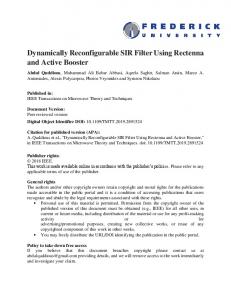
Fig. 2: DRESPA general system architecture be pipelined so that the interconnected resources can be pipelined. Therefore, to cater to the requirements of the real-time high-speed signal processing applications, the embedded architecture should be composed of arithmetic-operation-level configurable modules. Dynamically Reconfigurable Embedded Signal-Processing Architecture (DRESPA) is a novel architecture for reconfigurable embedded systems, targeted at applications with inherent data-parallelism, high regularity, and high throughput requirements. Given the nature of target applications, the reconfigurable component is organized as an array or reconfigurable cells (RCs). Since most of the target applications possess word-level granularity, the RCs are also coarse-grain. The embedded processor is an autonomous processing unit. It performs scalar operations and controls the operations of RC array. The reconfigurable unit performs vector operations under the control of the embedded processor. A specialized memory unit handles data transfers between external memory and the RC array, and stores input, intermediate and output data. Also, there is a separate memory for storing context data. It has a multi-level interconnection network that integrates the reconfigurable SIMD component within embedded processor to perform both parallel as well as sequential parts of an application. A dedicated I/O unit handles real-time data input and output. The general system architecture, shown in Fig. 2, comprises an embedded processor, a reconfigurable unit, a high bandwidth memory unit and input/output (I/O) unit, all implemented as a single chip. These system components are interconnected via four system buses consisting of two I/O buses and two memory buses. Two I/O buses are used to transfer data between Data Buffer and I/O unit; the two memory buses are used to transfer data between Data Buffer and reconfigurable unit. These four system buses allow the
Functional modification requires introducing new application software instead of incurring an expensive redesign. The same hardware architecture can be targeted to wide range of applications. Design using dynamically reconfigurable embedded architectures results in shorter time to market, productivity gains and reduced development costs.
Proposed architecture-Drespa: The major components of a dynamically reconfigurable embedded architecture are configurable processor, memory unit, cache unit and reconfigurable cell array. Real-time signal processing applications require the systems to have some form of pipeline processing. The idea of pipelining is to divide the execution of one instruction into steps, which are called pipeline stages. Each stage makes some contribution to the instruction and can operate in parallel with other stages. Pipelining improves performance by increasing instruction throughput. It does not decrease the time to execute individual instructions, but it will execute more instructions per time unit, resulting in speed up. All the pipeline stages must be built around memory. At one of the system-level pipeline stages, vector operations are performed on the input data in an execution unit. Computational resources must be shared among all the computational aspects of the application to make the amount of hardware reasonable. The interconnections of the computational resources need to be changed dynamically for different vector operations. All the interconnections of computational resources should form pipelines to support the pipelined vector operations; each computational resource also needs to 826
J. Computer Sci., 3 (10): 823-828, 2007 Fig. 4. The 1-D DCT algorithm is first applied to rows of an input 8×8 image pixel block. To the resulting matrix, 1-D DCT algorithm is applied to the columns to get 2-D DCT. The computation of 1-D DCT for 1 row requires thirteen multipliers and twenty nine adders. So, for 8 rows, 104 multipliers and 232 adders are required. Hence for 2-D DCT, 208 multipliers and 464 adders are required. In this architecture, two 8×8 blocks can be processed in parallel. Two 8×8 blocks are loaded from data buffer into RC array, with each pixel stored in one RC. The data bus between data buffer and RC array allows concurrent loading of sixteen pixels. So, eight clock cycles are required for loading two blocks. The same number of clock cycles is required to write out the processed data to the data buffer. Using properties of separable transforms, 1-D DCT along rows is computed. Then, 1-D DCT is computed along columns of resultant matrix. For one stage of butterfly computation, two clock cycles are required. So, for five stages, ten clock cycles are needed. Two clock cycles are required for buffering of data. This same twelve clock cycles is required for other 1-D DCT. Thus, for 2-D DCT computation of two 8×8 blocks, twenty four clock cycles are required. Additionally, eight clock cycles are required for loading of pixel values and eight clock cycles for writing out the processed data, totaling forty clock cycles. For a 256 x 256 grayscale image, there are 1024 blocks. In forty clock cycles two 8 x 8 blocks are processed. To process 1024 blocks, 20480 clock cycles are required. With 16-bit data, the throughput of 2-D DCT algorithm is given by:
Fig. 3: System-wide pipeline
Fig. 4: Fast eight-point 1-D DCT algorithm system to perform I/O operations and vector operations at the same time. Each bus can be used for any type of data transfer operation. In one of the typical system activities, the following data transfer operations might be performed in parallel: • • • •
I/O unit to data buffer: real-time data input. Data buffer to I/O unit: result data output. Data Buffer to Reconfigurable unit: Input for vector operations. Reconfigurable unit to data buffer: Output of vector operations.
Throughput =
The capability of these four parallel data transfer operations enables the system to operate globally in pipeline. The system-wide pipeline consists of five stages: the first stage for real-time data input, the second for reconfigurable unit data input, the third for vector operations, the fourth for reconfigurable unit data output, the fifth stage for result data output, as shown in Fig. 3.
8 x 256 x 256 bits/cycle 20480
In this algorithm, 192 (= ((2+1)×4)×8×2) operations are performed as vector computation and seventeen operations (eight input, eight output and one context switches) are performed by the processor. So, speedup is given by 17 ×S ≤1 209
RESULTS AND DISCUSSION
or S
The implementation of 2-Dimensional Discrete Cosine Transforms (2-D DCT) on DRESPA is discussed in this section. 2-D DCT is most widely used in video and image compression. The algorithm used for this implementation is a fast DCT algorithm[6] which is based on Discrete Fourier Transforms (DFT). The algorithm for fast eight-point 1-D DCT is shown in
12.3
The implementation results are summarized in Table 1. The context loading time is 512 clock cycles, and since there are a large number of computation cycles before the configuration is changed, this time is negligible. The performance is compared with a similar reconfigurable system, a superscalar processor and 827
J. Computer Sci., 3 (10): 823-828, 2007 Table 1. DRESPA Implementation of 2-D DCT Algorithm. Parameter Value Clock Period 13 nS Word length 16 bits Number of RCs 192 Throughput 1.9 G bits per sec Number of Clock cycles 20480 Number of operations for RC 192 Number of operations for Input 8 Number of operations for Output 8 Number of Context Switches 1 Maximum Speedup 12.30 Clock Cycles
one context was used for each application and a considerable speedup was obtained. The question of how many contexts is an optimal number is still unanswered. In case an application used more than two, a configuration allocation algorithm implemented in the compiler could be used to reduce the number of context reconfigurations. There is still a big gap between the hardware and the software. To close this gap, further investigation is necessary in the area of compilers for reconfigurable embedded systems. Specifically, a compiler is to be designed for the DRESPA system to fully exploit it. With such a compiler, a wider range of applications can be tested and the architecture’s features further explored. It is also desirable to study the behavior of the architecture in presence of operating system. As a final note, investigating the previously mentioned topics will lead to the development of a high performance reconfigurable system. After a complete study of the interactions between architecture, compiler and operating systems for reconfigurable systems, one would be able to determine the best track to follow in the reconfigurable world.
Remarc V830 R
400
320 sDCT
246 201
200
TMS320C80
54
DRESPA
24
0
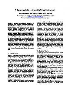
Fig. 5: Performance algorithm
comparisons
for
2-D
DCT
REFERENCES
commercial processors. Figure 5 shows the performance comparison in terms of number of clock cycles required for computation of 2-D DCT for one 8×8 block. REMARC[7] is another reconfigurable system targeting multimedia applications. It requires 54 clock cycles for computing 2-D DCT on one 8×8 block. V830 R/AV[8] is a superscalar multimedia processor requiring 201 clock cycles. sDCT[9] is a software implementation written in optimized Pentium assembly code using special MMX instructions, which requires 246 clock cycles. TMS320C80[10] is a commercial digital signal processor requiring 320 clock cycles. DRESPA requires 24 clock cycles to compute 2-D DCT on two 8×8 blocks. The existing major embedded architectures used for system design were reviewed and the increasingly important role that the dynamically reconfigurable embedded architecture will play in the future was discussed. The proposed architecture, DRESPA was described and multiple opportunities for run-time customization were discussed. Many of these technologies have reached relative maturity. Based on the applications in this work, it appears that the number of contexts does not need to be large to achieve good performance improvement with a Reconfigurable Unit. In these applications, more than
1.
Biswadip Mitra, 2002. Keynote Talks. Proceedings 15th International Conference on VLSI Design. 2. W.J. Trybula, 2003. Common Base on Mask-cost of ownership. SPIE(Photomask 2003) Proceedings. 3. Goldstein, S. et al., 1999. PipeRench: A Coprocessor for streaming Multimedia Acceleration. 26th Int. Symp. Computer Architecture, IEEE. 4. Brown, S. and J. Rose, 1996. FPGA and CPLD Architectures: a tutorial. IEEE Design and Test of Computers, 42-57. 5. Smith, M.J., 1997. Application-Specific Integrated Circuits. Pearson Education Inc., ISBN: 81-7808-007-9. 6. Natarajan, S., and N. Ramadass, 2005. Self-Modifiable Mixed-Signal SoC Architecture for Embedded Applications. National Conference on Signals, Systems and Communications (NCSSC 2005) Proceedings. 7. Chen, W.H., C.H. Smith and S.C. Fralick, 1977. A Fast Computational Algorithm for the Discrete Cosine Transform. IEEE Trans. on Communications, 25(9). 8. Miyamori, T. and U. Olukotun, 1997. A quantitative analysis of reconfigurable coprocessors for multimedia applications. IEEE Symposium on FPGAs for Custom Computing Machines, 2-11. 9. Arai, T., K. Nadehara and K. Suzuki, 1998. V830R/AV: Embedded Multimedia Superscalar RISC Processor. IEEE MICRO, 36-47. 10. Intel Application Notes for Pentium MMX. http://developer.intel.com/drg/mmx/appnotes. 11. F.Bonomini, G.A.Mian and D.Palumbo, 1996. Implementing an MPEG2 Video Coder Based on TMS320C80 MVP. SPRA 332, Texas Instruments.
828