design of application specific multiprocessor systems-on- chip. Our approach is based on a generic architecture model which is used as a template throughout ...
An Efficient Architecture Model for Systematic Design of Application-Specific Multiprocessor SoC A. Baghdadi, D. Lyonnard, N-E. Zergainoh, A.A. Jerraya TIMA Laboratory - Grenoble France possibility to scale the communication network on chip.
Abstract
This paper deals with the use of a generic architecture model for the design of application-specific multiprocessor systems-on-chip. The model used provides a great deal of modularity, flexibility and scalability. In the next section, we deal with the related works and outline our contribution. Section 3 introduces our generic architecture. The systematic design approach for multiprocessor systems-onchip is described in section 4. Section 5 details the design of an application-specific architecture for a packet routing switch. Section 6 is devoted to the evaluation of the architecture model and the associated design flow. Finally, section 7 provides our conclusions.
In this paper, we present a novel approach for the design of application specific multiprocessor systems-onchip. Our approach is based on a generic architecture model which is used as a template throughout the design process. The key characteristics of this model are its great modularity, flexibility and scalability which make it reusable for a large class of applications. In addition, it allows to accelerate the design cycle. This paper focuses on the definition of the architecture model and the systematic design flow that can be automated. The feasibility and effectiveness of this approach are illustrated by two significant demonstration examples.
2. Related Work and Contribution
1. Introduction
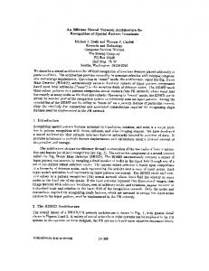
Figure 1 shows typical multiprocessor architectures as discussed in classical literature [6][19]. The model is made of a set of processors communicating through a communication network.
Current system design methods tend towards codesign of mixed hardware/software systems targeting multiprocessor system-on-chip. This direction is imposed by the ever increasing system-on-chip complexity. Additionally time-to-market pressure requires to shorten the design time, namely through raising the abstraction level of the specification entry. One of the most important issues in multiprocessor design is the target architecture. The rigidity of the target architecture may lead to a very restricted application field or poor performances. Modularity, flexibility and scalability are required to have an efficient application-specific multiprocessor design flow. What we mean here by efficient is the fact that it is feasible and applicable to large application fields with acceptable performances. Modularity is needed to master complexity. It allows the separate design of the different modules and provides an overall assembling scheme. The most common way to achieve modularity is to separate the inter-subsystem communication from the behavior when partitioning a system. Modularity allows for reuse of existing modules. Flexibility is required in order to avoid early decisions. It allows the designer to decide quite late in the design process which technology will be used for the design of each module. When combined with modularity, flexibility allows to change the implementation for a given module at any stage of the design process. For instance a software module may be converted into a hardware module for performance reasons. Scalability allows to adapt the same architecture model for applications of different complexity scales, e.g. increasing the number of processors or communication buses. For architecture design, modularity means separate design of inter-processors communication, flexibility requires the possibility to design application-specific interprocessors communication, and scalability requires the
Communication Network
Comm. Interface
Comm. Interface
Comm. Interface
Comm. Interface
ASIC
IP
Mem.
Mem. P
Figure 1. Generic architectural model as found in classical literature
A processor may be a specific CPU or an IP (memory, peripheral, specific hardware). The communication network constitutes the hardware links that support the communication primitives between components. The simplest way to connect the components of a system is to have a dedicated communication link between every two communicating components. The other extreme is to have a single bus connecting all the components. Between the fully connected network and the single bus solution, there is a wide range of interconnection networks. These networks are a major factor to differentiate modern multiprocessor architectures. A system architecture can vary from a simple controller to a massively parallel machine. Here what is interesting is the role played by each of the basic elements at the global control level of the system. We can classify system architectures into two categories: single-processor and multiprocessor architectures. A single-processor 1
architecture consists of one CPU and one or more ASICs. This scheme follows a master–slave synchronization pattern where the CPU acts as a top controller in charge of coordinating the activities of the other components which are acting as coprocessors. Although very useful in several application domains, the single processor architecture can only offer a restricted performance capability in many applications because of the lack of true parallelism. A multiprocessor architecture allows more flexibility and improved performances thanks to the distribution of computation among processors. However, it is much more difficult to handle due to parallelism. Several new simplified versions of this generic architecture were used for hardware/software codesign. Most of these works target single-processor architectures, and the most used model in this class is the single CPU single ASIC target architecture. Even though this architecture is a special and limited example of a distributed system, it is relevant in the area of embedded systems [15]. In this class of work we can cite LYCOS [14], COSYMA [18], and PMOSS [7]. Other design systems, such as Vulcan [11], TOSCA [1] and COBRA [12] can support more than one ASIC. Several research groups tried to target multiprocessor architectures, e.g. POLIS [2], Chinook [5], SpecSyn [8], CoWare [22][23] and the work led by Wolf and Ti-Yen [24]. In the POLIS [2] system, the target architecture is a system consisting of general-purpose processors combined with a few ASICs and possible other components such as DSPs. COSY [4] tried to extend this approach with a layered communication model. The target architecture in the SpecSyn [8] system is a heterogeneous multiprocessor with any number of processors, coprocessors, ASIP or FPGA, communicating through multiple buses. A more generic architecture was used in CoWare [23]. The authors presented an architecture and an associated design flow to target application-specific multiprocessor systems-on-chip. However, they restricted their communication model to point-to-point communication with “Rendez-vous” protocol. Besides these academic research projects, there were also several industrial trails of open standards and design methodologies [3][9][16][17][20][26][27][29][30][32] that try to deal with the more and more complex system on chip designs. However, we believe that in all above works, target architectures still lack generic aspects and thus only tackle a restricted application field. In fact, most of the above mentioned systems restrict the kind of components used and/or the communication network to few proprietary and/or specific models designed to be plugged together. The work presented in this paper allows the building of application-specific communication network (architecture) for heterogeneous multiprocessor system on chip.
The long-term objective is to use this model as a platform for the automatic generation of application-specific multiprocessor system-on-chip from a high-level specification.
3. A Multiprocessor Architecture Platform for Application-Specific System-on-Chip Design From the huge design space represented by figure 1 we chose the most appropriate elements that promote the adaptability for multiprocessor SoC design and the possibility of an automatic generation of the final architecture. The components of our architecture model belong to the three essential categories: software, hardware, and communication components. They consist of CPUs, hardware blocks, memories, and communication interfaces. Several kinds of CPUs may be used within the same design. The addition of an extra CPU requires the availability of a set of tools (ISS, compiler, debugger) and models (layout, timing, operating systems…). The current version of this work makes use of ARM7 and MC68000 CPUs. Of course the addition of new CPUs (e.g. DSP) will not change the principle of the approach. The communication network may be of whatever complexity from a single bus to a network with complex protocols. Processors are linked to the common network through communication interfaces. The scalability of this architecture depends on the scalability of the chosen communication network. Modularity is ensured by the use of specific interfaces to link processors to the communication network. This gives the possibility to design separately each part of the application, we can even include pre-designed modules (IPs). The generic assembling scheme of our model largely increases its modularity. This separation between processor and communication network through specific interfaces also provides high flexibility. In fact, if we change the technology implementing a given module (processor) the only part of the architecture that needs to be changed is the interface of the corresponding module. Figure 2 shows a typical instance of this platform made of N processors (ARM7 and MC68000 processors). The communication network is a point-to-point network. The choice of the processors was based on availability. These were the only two processors we had access to when we started this project. The architecture platform parameters that can be configured by the designer are the number of CPUs, the memory sizes for each processor, I/O ports for each processor and interconnections between processors, the communication protocols and the external connections (peripherals). These parameters show the scalability of the platform and enable the design of application-specific architectures of different scales. The communication interface depends on the processor attributes and on the application-specific parameters (communication structure).
The main contribution of this paper is the definition of a Modular, Flexible, and Scalable Architecture Model (MFSAM) that handles a large class of applications and may be used for an efficient multiprocessor SoC design flow. Additionally, this model allows for the systematic design of multiprocessor architectures. This will facilitate the development of automatic architecture generation tools. 2
�
�
�
�
�
�
�
�
�
�
�
�
�
�
�
�
�
�
�
�
�
�
�
�
�
�
�
�
�
�
�
�
�
�
�
�
�
�
�
�
�
�
�
�
�
�
�
�
�
*
�
�
+
�
,
,
�
�
,
�
�
�
�
�
�
�
�
�
�
�
�
�
�
�
�
�
The overall design flow from a system-level application model is shown in figure 5. Starting from a high-level model of the application at the system level (parallel communicating processes), and considering one multiprocessor architecture platform, the designer has to choose the adequate parameters of his final architecture. In this choice, the functional and non-functional constraints must be taken into account. A hardware/software codesign tool or a performance estimation tool can be used to assist the designer in his choice. The parameters that must be fixed in this step are the number of CPUs (of each available type), the memory sizes for each processor and the size of the shared memory if needed, I/O ports for each processor and interconnections between processors, the communication protocols and the external connections (peripherals). The results of this stage are two elements: an abstract architecture description and an allocation table. The abstract architecture constitutes the skeleton of the final SoC. It is an instance of the architecture platform and contains all the application specific parameters. The allocation table contains all the information about the memory map, the memory addresses and the interruption levels reserved for each CPU. Writing the allocation table requires a deep knowledge of the processors attributes (i.e. address space, interrupts levels).
�
�
�
�
�
�
�
-
�
�
�
)
�
�
�
�
�
(
�
�
�
�
�
�
�
�
�
�
�
�
�
�
�
Point-to-Point Network
! !
"
#
&
"
#
$
%
"
'
Figure 2 A multiprocessor architecture platform
In fact, the communication interface that we use to connect the processor to the communication network, is composed of two parts; one specific to the processor (interfacing its bus), and the other is generic and depends on the number of communication channels and communication protocols used. Figure 3 shows a generic model of a processor interface. Adr. Decoder
CPU bus
Adr. Decoder
Output Controller (Buffer, Protocol)
CPU - I/F
Comm. Network
Controller
Adr. Decoder
Rest Of System
Input Controller (Buffer, Protocol)
CPU dependent
Application dependent
Figure 3. Communication coprocessor
Fixed param. •Network type •Memory Arch. •CPU types
This decomposition in two parts allows to dissociate the CPU from the communication network. Each interface module acts as a coprocessor for the corresponding CPU. The application dependent part may include several communication controllers managing the communication through parallel channels. The arbitration is done by the CPU-dependent part. The overhead induced by this communication coprocessor depends on the design of the basic components and may be very low. As it will be explained later, the use of this architecture for interfaces provides huge flexibility and allows for modularity and scalability. Additionally, it allows for fast communication protocols (e.g. burst mode).
Application
Arch. Platform
system level description
Param. Choice (user constraints)
Pr. Attributes Library
Comm. I/F Library
Alloc. Table (Adr. & Rsrces.)
Abstract Archi. Descrp.
•Nb. of CPU •Comm. Prtocls. •Memory size •I/O for each CPU •Processors interconnects •External I/O
Archi. Design Detailed Archi.
Software Coding Binary Code for each Pr
Pr. & Mem. Simulators
Pr. & Mem. Cores
SoC synthesis
SoC Validation by cosimulation
4. Application-Specific Multiprocessor Systemon-Chip Design
Figure 5. MFSAM-based architecture generation flow for multiprocessor SoC
Our design flow follows the Y-chart [13][2] shown in figure 4, where the application-specific parameters are used to configure the architecture platform and an applicationspecific architecture is produced. These parameters result from an analysis of the application to be designed.
The architecture design step makes use of the allocation table to refine the abstract architecture and to produce the detailed architecture. The main action here is the design of the communication network including the processor communication interfaces. The software-coding step produces the programs which will run on each CPU. This may be a quite sophisticated step for large applications. This is true especially when an operating system is required to run the software. This step is out of the scope of this paper. The allocation table which was used to configure the communication interfaces, may be used for the software coding, for memory mapping and addresses allocation (I/O ports, interruptions). The results of this step are the binary codes that must be loaded onto the ROM of each processor. Of course, the operation of
Fixed parameters
•Network type •Memory Arch. •CPU types •Hw blocs
Component Library
Appli. specific parameters
Arch. Platform
Architecture Generation Tool
•Nb. of CPUs •Nb. Of Hw blocs •Memory size •I/O for each CPU •Processors interconnections •External I/O
SoC appli. spec. archi.
Figure 4. The Y-chart: MFSAM-based architecture generation scheme
3
communication protocol used for all of them is a FIFO protocol with handshaking. The three last columns depend on the chosen communication protocol. We can see that in this communication protocol, the FIFO is placed at the output channel and its size is equal to the transmitted frame size. For input channels (Ch_in_1 and Mode), the communication is done by interrupts; we use in this module the IRQ interrupt of ARM7 processor. In the last column of the table, we reserved the global addresses for the communication channels (see next section).
software coding is done separately for each processor. For the SoC validation, we need a cycle-accurate executable architecture that can run the application. To that end, we used a cosimulation approach [10] where CPUs are replaced by cycle accurate ISSs and bus functional models. All other parts of the architecture are modeled in VHDLRTL and executed by a VHDL simulator (e.g. Synopsys VSS [31]). Further illustrations about the validation of this flow will be given in the next section through a demonstration example.
Table 1. A 4-processor architecture description for the packet routing switch
5. Designing an Application-Specific Architecture for a Packet Routing Switch
Modules
CPU
Memory Comm. Comm. size channels Protocols
Interrupts
Adr.
In order to illustrate the efficiency of the proposed architecture model and design flow, we detail in this section the design process of a packet routing switch [28].
Buffer size (Hw)
Ch_in_1
0
IRQ*
0x7000
Input Controller 1 (IC1)
ARM7
ROM: 10 KB
0
IRQ*
0x7004
128 Bytes
-
0x7008
128 Bytes
-
0x700C
0
IRQ*
0x7000
0
IRQ*
0x7004
128 Bytes
-
0x7008
128 Bytes
-
0x700C
0
Level 5
0x9000
0
Level 6
0x9002
40 MHz RAM: 20 KB
Mode IC1 ⇒ OC1
FIFO at transmitter with HSK
IC1 ⇒ OC2 Ch_in_2
5.1. The packet routing switch
Input Allocation Controller 2 Table (IC2)
It constitutes a powerful solution for large-frame or cell-switching systems [28].The version we present here consists of two input controllers and two output controllers. Each of the controllers handles one communication channel. The communication links between input and output controllers are configured by an external signal to be direct or switched. Figure 6 shows the block diagram of the packet routing switch.
ARM7
ROM: 10 KB
40 MHz RAM: 20 KB
Mode IC2 ⇒ OC2
FIFO at transmitter with HSK
IC2 ⇒ OC1 IC1 ⇒ OC1
Output Controller 1 (OC1)
Output Allocation Controller 2 Table (OC2)
M68000 ROM: 20 KB
IC2 ⇒ OC1
20 MHz RAM: 20 KB
M68000 ROM: 20 KB
FIFO at transmitter with HSK
Ch_out_1
128 Bytes
-
0x9004
IC2 ⇒ OC2
0
Level 5
0x9000
IC1 ⇒ OC2
20 MHz RAM: 20 KB
FIFO at transmitter with HSK
Ch_out_2
0
Level 6
0x9002
128 Bytes
-
0x9004
-
-
-
Ch_in_1 .
.
/
0
4
5
6
3
Output Controller 1
0
/
0
1
2
0
3
External Environment (periphs.)
Input Controller 1 8
4
9
VHDL process 100 MHz
Mode Ch_in_2 Ch_out_21
FIFO at transmitter with HSK
Ch_out_2 :
* The address of the communication controller that requested the interruption will be delivered by the communication interface to the CPU when a read access is performed at the address 0x7100 .
/
0
4
5
6
0
7
Output Controller 2
Input Controller 2 .
/
0
1
2
0
This table will be used for the configuration of the communication interfaces and for the software coding (see figure 5). 7
Figure 6 Block diagram of the packet routing switch
5.3. Architecture design 5.2. Parameters extraction
As the architecture contains 4 CPUs, 4 communication interfaces must be designed. The interfaces of figure 3 are modeled in VHDL-RTL as a generic component that needs to be personalized according to the application. So for each of the 4 communication interfaces we analyze the parameters of table 1, and modify the VHDL files to obtain the specific interface. For example, in order to design the communication interface of the first module (IC1), the interface controller of ARM7 was selected and 4 communication controllers were instantiated (2 input controllers and 2 output controllers). The chosen communication controllers correspond to handshake protocol with buffering at the transmitter side. The size of the buffer was configured to 128 bytes (see table 1). The memory addresses of the communication controllers are also configured to the values mentioned in table 1. These addresses are also used to configure the address decoder which enables the corresponding communication interface (i.e. external accesses of the CPU). The result of this stage
From this specification we can note that we have 4 communicating modules, 4 internal communication channels and 5 external links. We know also that the input frame is 128 bytes long. The application was specified in the SystemC language. Thus, in order to implement this application on the proposed architecture platform, we started by choosing the application-specific parameters and writing (as result) the allocation table and the architecture description. We chose a 4-processor architecture as a first implementation. Table 1 shows the details of all the chosen parameters. In this table, each line contains the specific parameters of one module (processor) of the architecture. For example, in the first line we see that the IC1 module will be implemented on an ARM7 processor running with a 40 MHz clock frequency. The local memory size for this module was chosen approximately (after a first precompilation of the software part). There are 4 communication channels in this module, and the 4
is a VHDL component which represents the specific communication interface of the first module (IC1). Figure 7 shows the block diagram of this interface. We notice that input communication controllers use interrupts to communicate data to the CPU, so the interrupt controller must be configured to use the IRQ interrupt of the ARM7 as mentioned in table 1.
interrupts…). The results of this step are the binary codes that must be loaded onto the ROM of each processor.
5.5. Architecture validation In order to validate the generated architecture, we use a cycle accurate cosimulation approach based on SystemC [21][10]. In this approach, CPUs are replaced by cycleaccurate ISSs and bus-functional models. With this cosimulation tool we already have two cycle-accurate simulators, one for ARM7 (based on ARMulator) and the other for M68000. In addition, with these simulators, local memories are modeled in software as a part of the ISS, and the access to those memories is cycle accurate. Communication interfaces, communication network and the external environment (the test bench) were modeled in VHDL-RTL (cf. section 5.3). The VHDL part is executed by a VHDL simulator (e.g. VSS). We constructed the cosimulation environment which consists of 2 ARM7 ISSs, 2 M68000 ISSs and one VSS. Figure 8 shows the schema of the generated cosimulation environment.
Communication I/F 0x7000
CPU Memory Bus Adapter
Controller_in (FIFO+HSK) Req Ack F1
F2
Ch_in_1
Data
F3
ARM7 Core (IC1 Module)
RESET_n FIQ_N WAIT_N _N ALE RW_N BW_N M[4:0] DATA DOUT ADRESSE
F1
F2
F3
0x7004
F7
F1 F4
F6
Adr. Decoder
Controller_in (FIFO+HSK) Req Ack
F5
IT Controller
D A T A
F2
Mode
Data
F3
0x7008
B U S
Controller_out (FIFO+HSK) F1
F2
F3 Req Ack
F4
FIFO Channel Controller
0x700C
IC1 ⇒ OC1
Data
Controller_out (FIFO+HSK)
Clk F1
F2 F4
FIFO
F3 Req Ack
IC1 ⇒ OC2
Data
MC68k ISS
MC68k ISS
ARM7 ISS
ARM7 ISS
(OC2)
(OC1)
(IC2)
(IC1)
Mem. BFM
Figure 7 Communication Interface of IC1 Clk4
In the same way we constructed the 3 other communication interfaces. As all of these interfaces are VHDL components, we chose to gather all of them with the communication network (point-to-point connections) in one VHDL block. Table 1 is also used at this stage to determine the links between the 4 interfaces and their external links with the environment. In this example, the environment was a simple test bench which sends and receives the data packets, it was written in VHDL and uses the same communication protocol (i.e. handshake) as mentioned in table 1.
Mem. BFM
Mem. BFM
Clk3
Clk2
Mem. BFM Clk1
cosimulation bus (SystemC)
OC1 ⇐ IC2
OC2 ⇐ IC2 OC2 ⇐ IC1
OC1 ⇐ IC1 Cout1
Cin2
Cout2
mode Cin1
Env. (Test bench)
VHDL
Figure 8 A 4-processor cosimulation architecture of the packet routing switch
The cosimulation bus is based on SystemC and ensures the interconnection and synchronization of the running simulators (shared memory and monitors) for coherent execution of the overall system [21]. The binary codes were loaded onto the corresponding ISSs and the VHDL block was loaded onto the VSS. Figure 9 shows a snapshot of the running system.
5.4. Software coding We wrote simple test programs to run on each of the 4 processors. Each program makes use of read/write functions. An output operation corresponds to writing the corresponding data at the right address. For example, in module IC1, to transfer the received packet to module OC1 the packet is written (byte par byte) on the global address 0x7008. The communication interface buffers this data and takes charge of its transfer to module OC1. Input operations use interrupt events and require interrupt handlers. For example, for the IRQ handler of IC1 module, the CPU starts by performing a read access at the address 0x7100. When accessing this address, the interface delivers the address of the corresponding communication controller which requests the interrupt (0x7000 or 0x7004), and then the data is read at this received address. Note that this way of interrupt vectorisation is very useful when the number of the input communication controllers is greater than the available interruption levels of the CPU. In this example, the data packet was received byte by byte. These test programs were compiled and linked with the corresponding boot code for each CPU (to initialize the RAM/ROM, stacks, vectors,
MC68k ISS
ARM ISS
MC68k ISS ARM ISS
VHDL sim. VSS
VHDL signals
Figure 9 Executing the packet routing switch on a 4processor architecture
5
both architectures. In this case, the biggest difference comes from the area used for embedded CPUs (2 instead of 4). As expected, the cosimulation has shown that the throughput of the 4-processor architecture is twice as large as the 2processor solution.
6. Evaluation of the model and the associated design flow In order to analyze the efficiency of this model, we will use 2 other designs based on this architecture platform: A 2processor implementation of the packet routing switch and a 4-processor implementation of a DSP application – the IS95 CDMA protocol.
Table 3. Synthesis results of the two architectures implementing the packet routing switch
6.1. A 2-processor solution for the packet routing switch A 2-processor implementation of the packet routing switch was also realized following the same flow. Table 2 shows the allocation table for this new implementation. Only two CPUs are used: the two modules IC1 and IC2 are implemented on one ARM7 CPU, and the two other modules (OC1 and OC2) are implemented on one M68000 CPU. Therefore, only two communication interfaces had to be designed. These communication interfaces differ from the ones developed in the previous architecture by the number of communication controllers. So while building the communication interface of the ARM7 CPU, 7 communication controllers were instantiated (3 input and 4 output controllers). We modified the test programs to adapt them to this new architecture, and we validated the system by cosimulation.
CPU
Memory Comm. Comm. size channels Protocols
Buffer size (Hw)
Interrupts
Adr.
Input ARM7 ROM: 10 KB Controller 1&2 40 MHz RAM: 20 KB (IC)
Ch_in_1
0
IRQ*
0x7000
Ch_in_2
0
IRQ*
0x7004
Mode
0
IRQ*
0x7008
128 Bytes
-
0x700C
C2 (IC ⇒ OC)
128 Bytes
-
0x7010
C3 (IC ⇒ OC)
128 Bytes
-
0x7014
C4 (IC ⇒ OC)
128 Bytes
-
0x7018
C1 (IC ⇒ OC)
0
Level 3
0x9000
0
Level 4
0x9002
0
Level 5
0x9004
C1 (IC ⇒ OC)
FIFO at transmitter with HSK
C2 (IC ⇒ OC)
Output M68000 ROM: 20 KB Controller 1&2 20 MHz RAM: 20 KB (OC)
C3 (IC ⇒ OC) C4 (IC ⇒ OC)
FIFO at transmitter with HSK
0
Level 6
0x9006
Ch_out_1
128 Bytes
-
0x9008
Ch_out_2
128 Bytes
-
0x900A
VHDL process 100 MHz
-
-
-
Mode Ch_in_2 Ch_out_1
FIFO at transmitter with HSK
4-processor Architecture
2 ARM7 Cores 2 M68000 Cores
+ 6 FIFOs of 128 bytes
2-processor Architecture
1 ARM7 Cores 1 M68000 Cores
+ 6 FIFOs of 128 bytes
5156 Gates
3376 Gates
6.2. Analyzing the design cycle We designed an IS-95 CDMA protocol to analyze the duration of the design cycle. This experiment has shown that a multiprocessor architecture can be designed in about one week when all the components of the architecture platform are ready. In an IS-95 CDMA cellular phone system [25], the mobile station contains two CDMA baseband modems (Tx and Rx), a QCELP (Qualcomm Code Excited Linear Prediction) voice encoder (ENC) and decoder (DEC), and a call processor (CAP). Figure 10 shows the block diagram of the system. CDMA baseband signal
CDMA baseband signal
Modem: Rx A
B
C
DEC
CAP
Modem: Tx D
E
F
Voice_out dial pad display panel
ENC Voice_in
Figure 10 Block diagram of the IS-95 CDMA mobile station
In the forward traffic channel, the input frame (on voice_in channel) is 160 bytes long, the encoded frame is 44 byte, and the transmitted frame is 1536 byte. Although, many architectural solutions are conceivable, we chose to map this application on the same 4-processor architecture as the one used to implement the packet routing switch (we did not implement the call processor – CAP). In order to do that, we wrote the allocation table and the architecture description for the IS-95 CDMA application. Comparing with those of the packet routing switch, the communication architecture is slightly different. Also the FIFOs sizes in the communication controllers are different. Thus, we re-built the 4 new communication interfaces. Moreover, as a C++ version of the application was available, we prepared the 4 software programs that will run on the 4 CPUs and generated the corresponding binary codes. Figure 11 shows the cosimulation architecture we used to validate the
Ch_in_1
External Environment (periphs.)
Processor Cores
This example shows clearly the scalability of this model. This was obtained thanks to the flexibility of the communication interface and the modularity of the approach.
Table 2. A 2-processor architecture description for the packet routing switch Modules
Comm. I/F & Comm. Network
Architecture
Ch_out_2 * The address of the communication controller which requested the interruption will be delivered by the communication interface to the CPU when a read access is performed at the address 0x7100
In order to compare the 2 architectures, we synthesized the VHDL blocks corresponding to the interfaces for the two architectures. The synthesis results of the two architectures are shown in table 3. In both cases, the biggest part of the area is used for CPUs and memories. The additional logic amounts only to 5156 gates for the 4-processor architecture and 3376 gates for the 2-processor architecture. In both cases this represents less than 5% of the total chip area. The size of the memory used for communication remains the same for 6
application on its specific designed architecture. External modules –base station and user input/output– were modeled in SystemC. ;
I
J
B
B
=
K
F
?
@
A
ARM7 ISS H
B
;
>
?
A
C
MC68k ISS M em.
M em.
BFM
the architecture model we propose in this paper is far more generic than the architecture platform we used for the examples. This leads obviously to a huge application field. Other kinds of CPUs (and DSP cores) can be integrated and used in the same way. This shows the great flexibility and modularity of the proposed architecture model.
A
B
;
>
A
B
=
BFM
Clk
The modularity of our architecture model appears in the organization scheme, which consists of separated modules communicating through a communication network. It separates the behavior from the inter sub-systems communication. In addition, each module can be designed separately, an assembling scheme is provided to connect them efficiently and to enable the reuse of existing modules. This assembling scheme is quite structured and easily permits the reconfiguration of the architecture. Thus, the technology choice can be done late in the design process which leads to a great flexibility. The scalability of our architecture model is also achieved thanks to the assembling scheme. It depends on the scalability of the chosen communication network. This scalability allows to adapt the proposed architecture model to applications of different complexity scales. For instance increasing the number of processors or communication buses.
Clk
VSS C
Clk
J
B
B
=
K
A
B
=
M obile Station
Base Station
Figure 11 A 4-processor cosimulation architecture of the IS-95 CDMA
Table 4 gives the time needed to fit the IS95-CDMA application on the proposed multiprocessor platform using a 4-processor implementation. We have measured the time needed for each step of the generation flow of figure 5. We noticed that the time for manual generation depends on the number of processors (4 in this example), it is a linear function with slope 8 hours/processor. In fact, the manual generation is not only time consuming but also fastidious, as complex applications are still difficult to handle without tools assistance. It is worth noting that we assume that the designer has a good knowledge of the processors tool kits and the application when doing the manual generation. Otherwise you would have to add the time required to acquire this knowledge. In an automatic generation scheme, this knowledge will not be required though. The software coding step includes only system call insertion in an existing software code.
7. Conclusion In this paper, we presented a generic architecture model for application-specific multiprocessor system-on-chip design. The proposed model is modular, flexible and scalable. It permits a systematic generation of multiprocessor architectures for embedded systems-on-chip. This work is a promising step towards the definition of an efficient multiprocessor SoC design environment applicable to a large application domain. This paper focused on the definition of the architecture model and a systematic design flow that can be automated. The feasibility and effectiveness of this architecture model were illustrated by design examples showing the scalability of the model. We have also demonstrated that the use of such a model shortens significantly the design cycle of complex applications.
Table 4. Time needed to fit the IS95 CDMA on the multiprocessor platform Operation
Time Needed (Manual coding)
Param. Extrat. (Arch. Descrp. Allocation & Alloc. Table) Table
~ 2 hr x 4
Architecture Design
~ 2 hr x 4 + 2 hr
Allocation Software Coding Table
Allocation ~ 4 hr x 4 Table
References
Build the Cosim. Env
~ 8 hr
Total
~ 42 hr
[1] S. Antoniazzi, A. Balboni, W. Fornaciari, and D. Sciuto, “Hardware/Software codesign for embedded telecom systems”, In proceedings of ICCD'94, October 1994. [2] F. Balarin, E. Sentovich, M. Chiodo, P. Giusto, H. Hsieh, B. Tabbara, A. Jurecska, L. Lavagno, C. Passerone, K. Suzuki, and A. Sangiovanni-Vincentelli, “Hardware-Software Codesign of Embedded Systems – The POLIS Approach.”, Kluwer Academic Publishers, 1997. [3] R.A. Bergamaschi, and W.R. Lee, “Designing Systems-onChip Using Cores”, In the 37th Design Automation Conference, June 2000. [4] J-Y. Brunel, W. M. Kruijtzer, H. J. H. N. Kenter, F. Pétrot, L. Pasquier, E. A. de Kock, and W. J. M. Smits, “COSY Communication IP's”, In the 37th Design Automation Conference, June 2000.
6.3. Analysis of the results These examples illustrate the feasibility and the efficiency of our architecture model. With this model, multiprocessor architectures become much easier to handle. We illustrated how the generation of application-specific architectures can become systematic and very fast. Note that 7
[5] P.H. Chou, R.B. Ortega, and G. Borriello, “The Chinook hardware/software co-synthesis system”, In the 8th International Symposium on System Synthesis, September 1995. [6] D. Culler and J.P. Singh with A. Gupta, “Parallel Computer Architecture: A Hardware/Software Approach”, Morgan Kaufmann Publishers, August 1998. [7] G. H.J. Eikerling, W. Hardt, J. Gerlach, and W. Rosenstiel, “A Methodology for Rapid Analysis and Optimization of Embedded Systems”, International IEEE Symposium and Workshop on ECBS, D-Friedrichshafen, March 1996. [8] D.D. Gajski, F. Vahid, and S. Narayan, “A system-design methodology: Executable-specification refinement”. In the European Conference on Design Automation, February 1994. [9] M. Genoe, P. Delforge, and E. Schutz, “Experiences of IP Reuse in System-on-Chip Design for ADSL”, In the IEEE International Solid-State Circuits Conference, 1999. [10] P. Gerin, S. Yoo, G. Nicolescu, A.A. Jerraya, “Scalable and Flexible Cosimulation of SoC Designs with Heterogeneous Multiprocessor Target Architectures”, Submitted to ASPDAC, 2000. [11] R.K. Gupta, C. Coelho, and G. De Micheli, “Synthesis and simulation of digital systems containing interacting hardware and software components”, In the 29th Design Automation Conference, June 1992. [12] G. Koch, U. Weinmann, U. Kebschull, and W. Rosenstiel, “System prototyping in the COBRA project”, Journal on Microprocessors and Microsystems, Elsevier, vol.20, no.3, May 1996. [13] E.A. de Kock, G. Essink, W.J.M. Smits, P. van der Wolf, J.Y. Brunel, W.M. Kruijtzer, P. Lieverse, K.A. Vissers, “YAPI: Application Modeling for Signal Processing Systems”, In the 37th Design Automation Conference, June 2000. [14] J. Madsen, J. Grode, P.V. Knudsen, M.E. Petersen and A. Haxthausen, “LYCOS: the Lyngby Co-Synthesis System”, Design Automation for Embedded Systems, vol.2, n.2, 1997. [15] G. De Micheli, “Computer-aided hardware-software codesign”, IEEE Micro, 14(4):10-16, August 1994. [16] A. Niemegeers, G. de Jong, M. De Langhe, “Early system covalidation based on a hierarchical specification flow”, In the IEEE International High Level Design Validation and Test Workshop (HLDVT'99). [17] J. Notbauer, Th. Albrecht, G. Niedrist, and S. Rohringer, “Verification and Management of a Multimillion-Gate Embedded Core Design”, In the 36th Design Automation Conference, June 1999. [18] A. Österling, Th. Benner, R. Ernst, D. Herrmann, Th. Scholz, and W. Ye, “Hardware/Software Co-Design: Principles and Practice”, Chapter: “The COSYMA System”. Kluwer Academic Publishers, 1997. [19] D.A. Patterson and, J.L. Hennessy, “Computer Organization and Design: The Hardware/Software Interface”, Second Edition, Morgan Kaufmann Publishers, 1997. [20] A. Rincon, W. Lee and M. Slatery, “The Changing Landscape of System-on-a-Chip Design”, IBM MicroNews, 3rd Quarter 1999, Vol.5, No.3, IBM Microelectronics. [21] L. Semeria and A. Ghosh, “Methodology for Hardware/Software Co-verification in C/C++”, In the Asia South Pacific Design Automation Conference, January 2000.
[22] K. Van Rompaey, D. Verkest, I. Bolsens and H. De Man, “CoWare – A Design Environment for Heterogeneous Hardware/Software Systems”, In EURO-DAC’96, September 16-20, 1996. [23] S. Vercauteren, B. Lin and H. De Man, “Constructing Application-Specific Heterogeneous Embedded Architectures from Custom HW/SW Applications”, In the 33rd Design Automation Conference, June 1996. [24] T.Y. Yen and W. Wolf, “Communication synthesis for distributed embedded systems”, In International Conference on Computer Aided Design. IEEE Computer Society Press, 1995. [25] S. Yoo, J. Lee, J. Jung K. Rha, Y. Cho, and K. Choi, “Fast Prototyping of an IS-95 CDMA Cellular Phone: a Case Study”, In the 6th Conference of Asia Pacific Chip Design Language, pp. 61-66, October 1999. [26] ARM, Inc. “AMBA Specification Overview”, http://www.arm.com/Pro+Peripherals/AMBA [27] IBM, Inc. “Blue Logic Technology”, http://www.chips.ibm.com/bluelogic [28] IBM, Inc. “28.4G Packet Routing Switch”, Networking Technology Datasheets, http://www.chips.ibm.com/techlib/products/commun/datashee ts.html [29] IBM, Inc. “The CoreConnectTM Bus Architecture”, 1999, http://www.chips.ibm.com:80/news/1999/990923/pdf/corecon 128_wp.pdf [30] Sun Microsystems, Inc. “MAJCTM Architecture Tutorial”, white paper, 1999. http://www.sun.com/microelectronics/MAJC/ [31] Synopsys, Inc., “Synopsys VHDL System Simulator”, http://www.synopsys.com/products/simulation/vss_cs.html [32] VSI Alliance™, “VSI Alliance™ Architecture Document”, 1997, http://www.vsia.com/
8