An Efficient Hardware Architecture of a Scalable Elliptic Curve Crypto-Processor Over GF(2n ) Lo’ai Tawalbeh a , Alexandre Tenca b , Song Park and C ¸ etin Ko¸c
c
a Computer
c
Engineering Department, Jordan University of Science and Technology, Irbid, JORDAN;
[email protected] b Synopsys Inc., Hilsboro, OR, USA;
[email protected] School of Electrical Engineering and Computer Science,Oregon State University, Corvallis, OR, USA; parkso,
[email protected] ABSTRACT
This paper presents a scalable Elliptic Curve Crypto-Processor (ECCP) architecture for computing the point multiplication for curves defined over the binary extension fields (GF (2n )). This processor computes modular inverse and Montgomery modular multiplication using a new efficient algorithm. The scalability feature of the proposed crypto-processor allows a fixed-area datapath to handle operands of any size. Also, the word size of the datapath can be adjusted to meet the area and performance requirements. On the other hand, the processor is reconfigurable in the sense that the user has the ability to choose the value of the field parameter (n). Experimental results show that the proposed crypto-processor is competitive with many other previous designs. Keywords: Processor Architecture, Scalable Hardware, Division/Multiplication Algorithm, Cryptography, Galois Field Arithmetic, Point Addition.
1. INTRODUCTION Recently, there are many factors that force the need for secure communication. Among these factors are the continuous growth of the Internet, the electronic systems connection and the E-commerce transactions. The public-key Cryptography is widely used to ensure secure communication between different hosts. There are many common public-key cryptosystems such as ElGamal1 and RSA.2 In this paper, we will focus on the public-key Elliptic Curve Cryptosystem (ECC). ECC was introduced by Miler3 and Koblitz.4 The mathematical problem in which ECC is based, is more difficult to solve than the one used in traditional public key algorithms and thus, the same level of security can be obtained by using ECC with much smaller key sizes than traditional algorithms. For example a key size of 200 bits in an ECC has security level equivalent to 1400-bit RSA system.5 In this paper we present a scalable Elliptic Curve Crypto-Processor (ECCP) architecture to compute the point multiplication for the curves defined in the binary extension fields GF (2n ). The core arithmetic operation to compute the point multiplication is the modular multiplication. Montgomery Multiplication (MM) algorithm6 is an efficient way to compute modular multiplication. Many multiplier designs based in the MM algorithm were proposed.7–9 Also, the modular division and modular inverse are used to convert field elements between the projective and affine coordinates. These operations are very time consuming and increase the critical path delay of a design that implements them. The speed of the ECCP depends on how fast the arithmetic operations can be executed. The proposed ECCP architecture uses a simplified version of an algorithm (called UDMA) that is able to compute modular division and Montgomery modular multiplication in GF (2n ) and GF (p) (the algorithm is used for GF (2n ) only). This algorithm was already proposed and proved to be correct in another work.10 The proposed hardware architecture supports all the computation steps in the algorithm. The scalability feature of the proposed crypto-processor allows the adjustment of the word size used in the datapath to meet area and performance requirements. On the other hand, the processor allows the user to choose the value of the field parameter (n).
The following Section presents some mathematical concepts related to the ECC. The top level architecture of the proposed processor and its general operation are proposed in Section 3. The algorithm used to compute modular division and Montgomery modular multiplication is described in Section 4. The hardware description of the main components of the ECCP is presented in Section 5. The experimental results and conclusions are shown in Sections 6 and 7.
2. MATHEMATICAL BACKGROUND AND NOTATION This section provides a brief mathematical overview of the Elliptic Curve Cryptosystem (ECC). More details can be found in the literature.5, 11 Data in an ECC is represented as points on an elliptic curve, so called because they arose historically from the problem of computing the solutions for an equation of an ellipse. These curves have special characteristics and provide the base for particular arithmetic operations. In cryptography, we are interested in the elliptic curves defined over finite fields. In other words, the coefficients of the defining equation (F (x, y) = 0) are elements of GF (q), and the points on the curve are of the form P = (x, y), where x and y are elements of GF (q) that satisfy the equation. In addition, a point at infinity12 is defined. In this paper, we consider the elliptic curves defined over GF (2n ). This field has the advantage that the field elements are represented as n-bit values.
2.1. Arithmetic Operations on Elliptic Curve The core operation on ECC is the scalar point multiplication which consists of a certain number of point additions. When a point P defined on the curve is added to itself k times, it is very difficult to find what was P without knowing k. That is the characteristic that provides security to ECC. Q = kP = P + P + ... + P | {z }
(1)
k times n
The elliptic curves defined over GF (2 ) satisfy the equation: E : y 2 + xy = x3 + ax2 + b
(2)
where a, b ∈ GF (2n ) and b 6= 0. The addition law for two points in affine coordinates involves multiplication, division and squaring in the underlying finite field, as follows: As mentioned earlier, division is an expensive operation increases the area and limits the speed of an efficient hardware implementation for ECC. The proposed design uses a hardware algorithm that integrates the multiplication and division/inverse operations, in such a way that the multiplication speed is not significantly impacted. Such feature is important because multiplication is used most of the time. Let P1 = (x1 , y1 ) and P2 = (x2 , y2 ) be two points defined on the curve, then P3 = (x3 , y3 ) = P1 + P2 is defined when P1 = 6 P2 as: α=
y1 + y2 x1 + x2
x3 = α2 + α + x1 + x2 + a y3 = (x1 + x3 )α + x3 + y1 and when P1 = P2 (point doubling) as: α = x1 +
y1 x1
x3 = α2 + α + a y3 = (x1 + x3 )α + x3 + y1
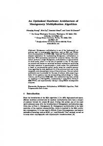
AU Control
Control Signals
USER
Main Control
AU Control
Register File
Data
Datapath
Data
Arithmetic Unit (AU)
Figure 1. Top Level Diagram of the Elliptic Curve Crypto-Processor (ECCP)
3. PROCESSOR ARCHITECTURE - TOP LEVEL The top level diagram of the Elliptic Curve Crypto-Processor (ECCP) is shown in Figure 1. Its components are the Arithmetic Unit (AU) data section and control, and the main control block. The main control block interacts with the user to get the scalar multiple (k) and the point to be multiplied (P ), passing them to the AU. The AU control block provides the necessary control signals to the AU data section in order to accomplish computing kP . The Arithmetic Unit is the place were all the field computations are performed. It consists of a datapath and a register file, as shown in the Figure. The datapath logic performs basic arithmetic operations and provides needed dataflow paths to compute modular division and Montgomery multiplication using the Unified modular Division and Multiplication Algorithm (UDMA)10 which will be discussed later. More details about the main components of the ECCP are provided in the following Sections. The idea of scalable architecture was introduced for Montgomery multiplication.7, 13 The objective of a scalable architecture is to be able to handle operands of various sizes by repetitive use of the same hardware core. Therefore, the scalable approach eliminates the fixed precision constraint imposed on other specialized designs.14, 15 This characteristic is important for a flexible crypto-processor architecture. The limit on the maximum size of the precision for the scalable design is governed by the available memory that stores the inputs and internal results. Given a sufficient amount of memory space, a scalable unit can perform computation on 32-bit or 128-bit values. Moreover, the scalable architecture concepts provides a generic hardware model that enhances portability across different hardware platforms. For instance, a Field Programmable Gate Array (FPGA) with limited area may use a smaller datapath in order to have the whole system fitting into the FPGA. If performance is the primary concern, then larger datapath version can be implemented for speed.16
3.1. General ECCP Operation Given a scalar multiplication the main control activates the AU to perform the basic operations of addition, multiplication, squaring, and division. The control of each basic operation is performed by the AU control. The main control passes the operands to the register file and activates the AU control. Once complete, the main control load new operands, read results, and activate new basic operations, until the scalar multiplication is complete. There is no specialized hardware for squaring, and the multiplier is used for this purpose.
Inputs: 0 ≤ X < p, 0 < Y < p, 2n−1 < p < 2n , F ield, Op, n Output: Z = XY 2−n mod p when Op = mult, Z = X Y mod p when Op = div Algorithm: IF Op = mult THEN /* M ultiplication M ode */ D = 0, U = 0, W = X, C = Y , δ = n ELSE /* Division M ode */ D = p, U = X, W = 0, C = Y , δ = 0 END IF; WHILE [(C 6= 0 AND Op = div) OR ( δ 6= 0 AND Op = mult)] IF c0 = 0 THEN C := C >> 1 δ := δ − 1 /* Integer Operation */ ELSE IF (Op = div) THEN IF δ < 0 THEN C ⇔ D, U ⇔ W , δ := −δ END IF; END IF; δ := δ − 1 C := (C + D) >> 1, U := (U + W ) END IF; U := (U + u0 ∗ p) >> 1 END WHILE; IF Op = div THEN Z := W ELSE Z := U END IF;
Figure 2. Simplification of Unified Modular Division/Multiplication Algorithm (UDMA) to work on GF (2n ) only
The AU can be seen as a hardware support for the field operations, with specific instructions to allow the activation of these operations, data transfers (to and from the register file), and status verification. A detailed list of these instructions is beyond the scope of this work.
4. ALGORITHM FOR MODULAR DIVISION AND MONTGOMERY MULTIPLICATION The datapath is responsible for the operations needed to accomplish the scalar point multiplication according to the ”Double and Add” point multiplication algorithm in the projective coordinates shown in.12 The AU architecture is defined by an algorithm for unified modular division/multiplication, which was devised and proved to be correct in.10, 17 Unified implies the algorithm to be functional in both prime GF (p) and binary extension field GF (2n ), also referred to as being dual field. In this work we are interested in GF (2n ) field only, since the unified architecture has some unavoidable overhead. The algorithm is an extension of the unified division algorithm presented in another work18 and combines the Montgomery multiplication and modular division in a single flow, maximizing the reuse of the same data path. The tradeoff involves an increase in control complexity. The pseudo code that represents the simplified version the algorithm in17 to work in GF (2n ) only is shown in Figure 2. Notice that modular inverse calculation is possible by forcing the numerator to a value of one during a modular division operation. The full version of the algorithm was completely implemented (including control signal timing and datapath structure) and described in.10 There the reader can obtain more details of the unified and scalable design, together with performance analysis for the algorithm. This paper describes a simpler and more efficient architecture that works for GF (2n ) only. The simplified UDMA mode of operation is controlled by input Op (div or mult). For simplicity, the polynomials X(x), Y (x), and p(x) are denoted as X, Y , and p, respectively, which corresponds to the bit-vector representation of these polynomials. The algorithm integrates the Extended Binary GCD algorithm and the Montgomery multiplication algorithm. To compute Montgomery multiplication, the algorithm performs n iterations. The counter δ is initialized with value n, and in each iteration it is decremented by one. The variables used in the algorithm are initialized as: C = Y , D = 0, U = 0, and W = X. The result is ready (Z = U ) when δ = 0. The partial product U is reduced
mod the field polynomial p in each iteration. While multiplying, addition is used in the operations that update C and D. The >> operator indicates a 1-bit right shift operation. The simplified UDMA computes modular division using the same structure used by the Extended Binary GCD Algorithm for modular division.18 The variables are initialized as: C = Y , D = p, U = X, W = 0, and δ = 0. The division is completed when C = 0, and the final result is available in W . The unified division/multiplication algorithm (UDMA) proposed in10 has certain operations that performed in (GF (p) only and under certain conditions. These operations are time consuming (such as addition with carry). In GF (2n ), there is no carry since the addition in this field is accomplished by bit-wise XORing. As a result, the simplified version of the UDMA has simpler operations and control flow which yields to a more efficient datapath implementation.
5. EECP HARDWARE DESCRIPTION The ECCP architecture was coded in VHDL. Every module was described using generic parameters, such that the size of the architecture can be set to any desired value. Since we are proposing a scalable architecture, there are some issues that need to be clarified before the details about the EECP implementation are presented.
5.1. Data Dependency Between Words In order to provide a word-by-word operation the input operands are divided into groups of smaller bit length, referred in this text as words. For example, a 1024-bit value can be divided into two 512-bit words. Since the algorithm contains right shifts, there is a dependency between consecutive words. Figure 3 illustrates the information exchange needed to achieve a correct full-precision result. Upper Word
Lower Word LSB
Overlap Bit
MSB
Figure 3. Data dependency between operand Words.
A bit value at a position that is one bit higher than the most significant bit of the current word needs to be extracted for a correct right shift operation. This bit corresponds to the least significant bit of the next consecutive word. During arithmetic right shift of individual words, the bit value to be shifted into its most significant bit position cannot be determined without the information from the connecting higher word. Considering the most significant bit of a word as a sign bit and shifting accordingly leads to an incorrect result. It is important to realize that the most significant bit of a word within the scalable design does not represent the most significant bit of the full-precision result. This extra bit is referred to as an ”overlap bit” because the value is read twice in an overlapped fashion. Acquiring overlapped bit occurs inside the register file. The bit tapping memory system has an extra output that extracts the least significant bit from the next consecutive word, which is illustrated in Figure 4. Consequently, the size of the scalable datapath is expended by one bit to include this overlap bit.
Precision = 16 bits Word = 8 bits Word 1
Word 0
MSB
1
LSB
8
Overlap Bit
Data Out
Figure 4. Overlap Bit Extraction.
5.2. Multi-word operation The control flow in the algorithm is determined by the least significant bit of the full precision operand value, which is used to test even condition (c0 = 0). Following this observation, the logical word flow of the scalable architecture begins with the least-significant (LS) word and move on to most-significant words, as shown in Figure 5. The true LS bit of an operand is saved into a register such that the higher words can follow the same control flow in the algorithm.
Begin Last Word
Intermediate Word
Intermediate Word
MSB
First Word LSB
n precision
Figure 5. Word Execution Sequence.
5.3. Partial Zero Detection Since the ECCP operates on words of the full-precision operand, checking for zero condition is tested in a partial manner. The word-based version of the zero detection unit is composed of a pass or fail register in addition to zero test logic. The zero test logic checks if the word under execution matches the zero condition. The pass or fail register retains the zero test information throughout different word executions.
5.4. Register File The register file serves as a storage space for initial, intermediate, and final data results. The register file consists of one input and two output ports, which can be viewed as a synchronous dual port memory. Dual output ports supply two input values to the datapath for computation and the computed result is written back to the register file. Both read and write timing of the memory is synchronous with the clock signal. For simplicity, the architecture of single operand is provided in Figure 6, showing the access to the overlap bit. With the aim to reduce unnecessary register space, the address bit length and the total number of addresses can both be specified. For example, an address bit length of three can allow maximum of 23 = 8 addresses, but if only five addresses are needed then it is possible to create five addresses by initial user setting. As a requirement of supporting the scalable architecture, the register file is capable of reading the overlap bit in addition to reading a specified word.
Register File
m < n
MSB
LSB
m < n
Data In
m
Data Out
1
m 1
m 1
m 1 1
Overlap Bit
Read Addr
Figure 6. Register for Multiple-word Operand - Component of the Register File.
5.5. Datapath The datapath is responsible for data transfers and manipulations. Multiplexers direct dataflow and slightly modified full adders manipulate input values. An adder is capable of computing addition in GF (2n ). Extra logic gate for a full adder in conjunction with small increase in control unit permits the design to operate in GF (2n ) and GF (p) fields. Figure 7 displays the layout of the m-bit datapath (m ≤ n) implementing the simplified UDMA. Each “while iteration” of the algorithm is implemented in one clock cycle for multiplication mode, and in three clock cycles for division mode if C is odd, and 2 clock cycles if C is even. The proposed datapath has two inputs which receive their values from the output ports of the register file. The main components of the datapath are the two adders, the results hif ter and the Y shif ter. The Yshifter shown in Figure 7 is a shift register that is used to implement the 1-bit right shift operation (C >> 1) only in the multiplication mode. The Yshifter is loaded with the input Y (multiplier) when laodY = 1. In both cases when C (remember that C = Y ) is even or odd, it is shifted right by 1-bit when shif tY = 1. The least significant bit of the shifted C goes to the control section to perform the test c0 = 0. The output of the datapath is shifted 1-bit to the right by correct wiring. The result shif ter at the output of the second adder is used to choose between the output and its shifted value. This module is implemented as 2-input multiplexers with select line shif t. When shif t = 1, the shifted output is selected. The MUX shown on top of Adder1 in Figure 7 is used to select between the value 0 or W depending weather C is even or odd (depending on c0 ), respectively. On the other hand, the multiplexer shown at the top of Adder2 is used to select between the value 0 or the modulus P depending weather U is even or odd (depending on u0 ), respectively.
5.6. Control The major component in the control unit is a finite state machine which was implemented using a hardwired control methodology. With the intention to design a robust and reliable control unit, the state machine was coded as a Moore machine where the output signals depend solely on the present state, this way minimizing or eliminating glitches.
Table 1. The critical path delay of the ECCP in nano-seconds for operand precision form (16-512) bits and different datapath word sizes
DELAY (nano-seconds) P recision(bits) 16-bit 32-bit 64-bit 128-bit 256-bit 512-bit
16 17.2 17.6 17.6 17.5 16.5 16.7
Datapath 32 64 17.8 19.2 20.4 19.2 20.8 19.1 20.7 18.2 20.7
word size 128 256 20 20.4 19 20.5 19.5
512 20.2
The algorithm’s swap functions (C ⇔ D and U ⇔ W ) are accomplished within control unit to avoid actual data transfer between registers. An actual transfer of data would be costly in terms of time, especially for a system with large precision. Thus, the swap is performed exchanging the addresses of the register in question, inside the control unit. Another important component of the control unit is the delta counter. This counter is used to control the swapping operation and the major algorithm control flow. The functionality for delta counter includes decrementing and negating the count value. With the goal of implementing a fast counter, a ring counter design was chosen. The delay of the ring counters are independent of size.19
6. EXPERIMENTAL RESULTS AND ANALYSIS The experimental data presented in this Section were generated using Mentor Graphics CAD tools. The target technology was set to AM I05 f ast auto (0.5 µm CMOS with hierarchy preserved) provided in the ASIC Design Kit (ADK) from the same company..20 The scalable architecture of the Elliptic Curve Crypto-Processor (ECCP) was described in VHDL and simulated in M odelSim to validate functional correctness. It was synthesized using Leonardo synthesis tool for the available technology. ADK provides a consistent environment for comparison between the designs, and a reasonable approximation of the system performance when using commercial ASIC technology. Table 1 shows the critical path delays (in nano-seconds) of the ECCP for the precision range from 16 bits to 512 bits at different combinations of the datapath word size (form 16 to 512 bits). From the delay Table, we can see that at word size 16, the critical path delay of the ECCP at operand precision of 16 bits is 17.2 nsec, at 256 it is 16.5 nsec, and at 512 bits it is around 20.7 nsec. We also notice that the minimum delay happens when the datapath word size is 16. When the word size increases the delay increases slightly for a fixed operand precision, and the delay increases as the number of bits increase and it saturates at higher precision. The proposed architecture that implements the simplified modular multiplication algorithm (UDMA) shown in Figure 2 performs one iteration of the algorithm in each clock cycle when computing Montgomery multiplication. This means that we need n cycles to compute Montgomery modular multiplication. The ECCP has no dedicated hardware for squaring (x2 ), and therefore the multiplication algorithm is used for squaring. On the other hand, it takes a maximum of 2 iterations/bit and on average 1.5 iterations/bit to compute the modular inverse in GF (2n ) using the simplified algorithm. The ECCP architecture performs each iteration of the algorithm in 2 clock cycles on average (one to compute C + c0 .D) and another to compute U + W with the modulus reduction). Therefore, the GF (2n ) inversion by the simplified algorithm takes on average 1.5 × 2 = 3 cycles for each bit. In computing kP using the double-add method,12 where P=(X1 , Y1 , Z1 ), Q=(X2 , Y2 , Z2 ) are points on the curve in the projective coordinates, we can assume that Z2 = 1, Computing point addition (P 6= Q) requires 13 field multiplications and computing point doubling (P = Q) required 7 field multiplications.21 To compute the
Table 2. The total area of the ECCP in gates for operand precision form (16-512) bits and different datapath word sizes
AREA (Gates) P recision(bits) 16-bit 32-bit 64-bit 128-bit 256-bit 512-bit
16 3857 4251 5012 6389 8212 12602
32 5567 6267 7664 10310 13861
Datapath 64 8945 10265 12928 18109
word size 128 256 15727 18274 29434 23473 34458
512 56570
scalar point multiplication (kP ) using equation 1, n point doubling operations are needed (n is the order of the field), and approximately n/2 point additions are needed (given that the number of 1’s in the binary expansion of k is 0.5n). Let the total average computation time of a given design to compute multiplication or division be Tdesign which is given by: Tdesign = (cycles/bit) ∗ n ∗ clock period. At operand precision of n= 512-bits, the time required to compute one multiplication by the ECCP is Tmult = 1 ∗ 512 ∗ 20.2 ∗ 10−9 = 10.3µsec. Then at n= 512-bits, the ECCP computes point addition in: TP Add = 13 ∗ Tmult ≈ 134µsec and half of that time is required to compute point doubling TP Double = 0.5 ∗ TP Add . To compute the scalar point multiplication (kP ), an inversion operation is required to transform back the result form the projective to the affine coordinates. The total time to compute the modular division (inverse) by the ECCP is Tinv = 3 ∗ Tmult ≈ 31µsec. Then, the total time to compute kP by the proposed ECCP is: TkP = 0.5n ∗ TP Add + n ∗ TP Double + Tinv = 13/2n ∗ Tmult + 7n ∗ Tmult + 3Tmult = (13.5n + 3) ∗ Tmult = (13.5n + 3)(n ∗ clock period) = (13.5n2 + 3n) ∗ clock period At precision n= 512-bits, TkP = 71 m sec. The proposed ECCP computes the kP faster than previously proposed elliptic curve architectures. As an example, the FPGA implementation of the Elliptic Curve processor presented in22 computes the scalar point multiplication in 80.3 m sec at operand size of 163-bits. Also, the ECCP has an advantage over other design by being scalable. I.e., the user can choose the word size to achieve the required performance. Table 2 shows the total area (in number of gates) for the ECCP design as a function of operand precision and different datapath word size. The area for the ECCP design was extracted from the experimental data presented in Table 2 as: AECCP = 236.12 ∗ n + 180 = O(n) gates Form the above Table, we can see that the proposed ECCP has area complexity of O(n) at a given datapath word size. This results is compatible with many other designs23, 24
7. CONCLUSION In this work we present an Elliptic Curve Crypto-Processor (ECCP) architecture to compute point multiplication in GF (2n ). The speed of the crypto-processor depends on the arithmetic operations performed in the underlying field. So, we used a new efficient algorithm to compute modular division and Montgomery modular multiplication. The divider/multiplier that implements this algorithm is very efficient and has a scalable datapath that can handle operands of any size. Also, the word size of the datapath can be adjusted to meet the area and performance requirements. Experimental results show that the total time required to compute scalar point multiplication is 71 m sec at 512-bit operand precision. This result is competitive with many other dedicated solutions.
REFERENCES 1. T. ElGamal, “A public key cryptosystem and signature scheme based on discrete logarithms,” IEEE Trans. - Information Theory IT-31, pp. 469–472, July 1998. 2. L. Adleman, R. L. Rivest, and A. Shamir, “A method for obtaining digital signature and public-key cryptosystems,” Comm. of the ACM 21, pp. 120–126, February 1978. 3. V. S. Miller, “Elliptic curves in cryptography,” in Advances in Cryptology Crypto’85, pp. 417–246, Lecture Notes in Computer Science No. 218, Springer-Verlag Berlin, Germnay, 1985. 4. N. Koblitz, “Elliptic curve cryptosystems,” Mathematics of computation 48, pp. 203–209, January 1987. 5. I. Blake, G. Seroussi and N. Smart, Elliptic curves in cryptography, Cambridge University Press, UK, First ed., 1999. 6. P. L. Montgomery, “Modular multiplication without trial division,” Mathematics of Computation 44, pp. 519–521, April 1985. 7. E. Savas, A. F. Tenca, and C ¸ . K. Ko¸c, “A scalable and unified multiplier architecture for finite fields GF (p) and GF (2m ),” in Cryptographic Hardware and Embedded Systems — CHES 2000, C ¸ . K. Ko¸c and C. Paar, eds., Lecture Notes in Computer Science, No. 1717, pp. 281–296, Springer, Berlin, Germany, 2000. 8. Alexandre F. Tenca and Lo’ai A. Tawalbeh, “An efficient and scalable radix-4 modular multiplier design using recoding techniques,” in The Thirty-seventh Annual Asilomar Conference on Signals, Systems, and Computers, pp. 1445–1450, IEEE Press, Pacific Grove, California, November 9-12, 2003. ¸ . K. Ko¸c, “High-radix design of a scalable modular multiplier,” in Cryp9. A. F. Tenca, G. Todorov, and C tographic Hardware and Embedded Systems — CHES 2001, C ¸ . K. Ko¸c and C. Paar, eds., Lecture Notes in Computer Science, No. 1717, pp. 189–206, Springer, Berlin, Germany, 2001. 10. Lo’ai. A. Tawalbeh, A novel unified algorithm and hardware architecture for integrated modular division and multiplication in GF (p) and GF (2n ) suitable for public-key cryptography. PhD thesis, Oregon State University, Oregon,USA, October 2004. 11. W. Trappe and L. C. Washington, Introduction to Cryptography with Coding Theory, Prentice Hall, New Jersey, 2002. 12. P1363, “Standard specifications for public key cryptography (draft vrsion 13), IEEE, November 1999.” 13. A. F. Tenca and C. K. Koc, “A word-based algorithm and scalable architecture for montgomery multiplication,” in Cryptographic Hardware and Embedded Systems — CHES 1999, C ¸ . K. Ko¸c and C. Paar, eds., Lecture Notes in Computer Science, No. 1717, pp. 94–108, Springer, Berlin, Germany, 1999. 14. A. Vandemeulebroecke and et al, “A new carry-free decision algorithm and its application to a single-chip 1024-b rsa processor,” IEEE Journal of Solid-state Circuits 25, pp. 748–755, June 1990. 15. A. Royo, J. Moran, and J. C. Lopez, “Design and implementation of a coprocessor for cryptography applications,” in European Design and Test Conference, pp. 213–217, (Paris, France), March 17-20 1997. 16. S. Park, “Hardware design of scalable and unified modular division and Montgomery multiplication,” Master’s thesis, Oregon State University, Oregon, USA, June 2005.
17. Lo’ai. A. Tawalbeh and Alexandre. F. Tenca, “An algorithm and hardware architecture for integrated modular division and multiplication in GF (p) and GF (2n ),” in The In The IEEE 15th International Conference on Application-Specific Systems, Architecture, and Processors (ASAP), pp. 247–257, ieeecs, September 2729, 2004. 18. Alexandre F. Tenca and Lo’ai A. Tawalbeh, “ An algorithm for unified modular division in GF (p) and GF (2n ) suitable for cryptographic hardware,” IEE Electronics Letters 40, pp. 304–306, March 2004. 19. M. Stan, A. Tenca, and M. Ercegovac, “Long and fast up/down counters,” IEEE Transactions on Computers 47, pp. 722–734, July 1998. 20. ASIC Design Kit. Mentor Graphics Co, “http://www.mentor.com /partners/hep/AsicDesignKit/dsheet/ami05databook.html.” 21. G. B. Agnew, R. C. Mullin, and S. A. Vanstone, “An implementation of elliptic curve cryptosystems over GF (2155 ),” IEEE Journal on Selected Areas in Communications 11(5), pp. 804–813, 1993. 22. G. Orlando and C. Paar, “Implementation of elliptic curve cryptographic Coprocessor over GF (2m ) on an FPGA,” in Cryptographic Hardware and Embedded Systems — CHES 2000, C ¸ . K. Ko¸c and C. Paar, eds., Lecture Notes in Computer Science, No. 2162, pp. 25–40, Springer, Berlin, Germany, 2000. 23. J. Goodman and A. P. Chandrakasan, “An energy-efficient reconfigurable public-key cryptography processor,” IEEE Journal of solid-state circuits 36, pp. 1808–1820, November 2001. 24. J. Wolkerstorfer, “Dual-field arithmetic unit for GF (P ) and GF (2n ),” in Cryptographic Hardware and Embedded Systems — CHES 2002, B.S. Kaliski Jr. et al., ed., Lecture Notes in Computer Science, No. 2523, pp. 484–499, Springer, Berlin, Germany, 2003.
W
Zero
U
Y
(c 0)
MUX
Adder1 P
LoadY shiftY
Zero
Yshifter LSBit of U (u 0 ) (c 0)
control
MUX
Adder2
result_shifter U Figure 7. The Datapath of The ECCP.
sh
shift