IEEE TRANSACTIONS ON VERY LARGE SCALE INTEGRATION (VLSI)
SYSTEMS. VOL. I. NO. 2, JUNE 1993 network the number of extra stages can be
...
IEEE TRANSACTIONS ON VERY LARGE SCALE INTEGRATION (VLSI) SYSTEMS.VOL. I. NO. 2, JUNE 1993 network the number of extra stages can be arbitrarily chosen whereas the number of stages in the multibuttertly is completely determined by the system size and the dilation factor.
171
An Efficient Logic Emulation System Joseph Varghese, Michael Butts, and Jon Batcheller
REFERENCES G. B. Adams, D. P. Agrawal and H. J. Siegel, “Fault-tolerant multistage interconnection networks,” Computer, vol. , pp. 14-27, June 1987. G. B. Adams and H. J. Siegel, “The extra stage cube: a fault-tolerant interconnection network for supersystems,’’ IEEE Trans. Computers, vol.
C-31, pp. 443-454, May 1982. D. M. Dias and M. Kumar, “Preventing congestion in multistage interconnection networks in the presence of hotspots,” in Int. Conj on Parallel Processing, pp. 19-11 3, 1989. A. Gottlieb, R. Grishman, C. P. Kruskal, K. P. McAuliffe, L. Rudolph arid M. Snir, “The NYU ultracomputer-designing an MIMD shared memory parallel computer,” IEEE Trans. Computers, vol. C-32, pp. 175-189, Feb. 1983. P. Kermani and L. Kleinrock, “Virtual cut-through: A new computer communication switching technique,” Computer Networks, vol. , pp. 267-286, Sept. 1979. T. Knight, A. DeHon, and H. Minsky, “Fault-tolerant design for multistage interconnection networks,” in Int. Symp. on Shared Memory Multiprocessing, pp. 60-7 I , 199I . S. Konstantinidou and E. Upfal, “Experimental comparison of multistage interconnection networks,” IBM Research Report, RJ 845I , November 1991. A. Ho, R. Cypher, S. Konstantinidou and P. Messina “Architectural requirements of parallel scientific applications with explicit communication,” IBM Research Report, RJ 9079, Nov. 1992. L. Kurisaki and T. Lang, “The performance of faulty multistage interconnection networks with diverting switches and correction links,” Inr. Conj on Parallel Processing, vol. I, pp. 190-193, 1990. T. Lang and L. Kurisaki, “Nonuniform traffic spots (NUTS) in multistage interconnection networks,” Int. Conj on Parallel Processing, pp. 191-195, 1988. T. Leighton and B. Maggs, “Expanders might be practical: fast algorithms for routing around faults on multibutterllies,” in Proc. 30th Ann. Symp. on Foundations of Computer Science, pp. 384-389, 1989. D. Mitra and R. Cieslak, “Randomized parallel communications,” in Int. Con5 on Parallel Processing, pp. 224-230, 1986. G. F. F’fister, W. C. Brantley, D. A. George, S. L. Harvey, W. J. Kleinfelder, K. P. McAuliffe, E. A. Melton, V. A. Norton and J. Weis, “The IBM research parallel processor prototype (RP3): introduction and architecture. Int. Con5 on Paralel Processing, pp. 76477 I , 1985. G. F. Pfister and V. A. Norton, “Hot-spot” contention and combining in multistage interconnection networks,” IEEE Trans. Computers, vol. C-34, pp. 943-948, 1985. S. L. Scott and G. S. Sohi, “Using feedback to control tree saturation in multistage interconnection networks,” in 16th Int. Symp on Computer Architecture, pp. 167- 176, 1989. Y. Tamir and G. L. Frazier, “High-performance multi-queue buffers for VLSI communication switches,” in Proc. 15th Int. Symp. on Computer Architecture, pp. 343-354, 1988. Y. Tamir and G. L. Frazier. The design and implementation of a multiqueue buffer for VLSI communication switches,” Int. Conj on Computer Design, pp. 466471, 1989. E. Upfal. “An O(10.gS )deterministic packet routing scheme,” in Proc. 21st Symp. on Theory of Computing, pp. 24 1-250, 1989. L. G. Valiant and G. J. Brebner, “Universal schemes for parallel communication,” in ACM Proc. 13th Symp. on Theory of Computing, pp. 263-277, 1981.
Abstract-The Realizer is a logic emulation system that automatically configures a network of Field-Programmble Gate Arrays (FPGA’s) to implement large digital logic designs. Logic and interconnect are separated to achieve optimum FPGA utilization. Its interconnection architecture, called the partial crossbar, greatly reduces system-level placement and routing complexity, achieves bounded interconnect delay, scales Iinearly with pin count, and allows hierarchical expansion to systems with hundreds of thousands of FPGA devices in a fast and uniform way. An actual multiboard system has been built, using 42 Xilinx XC3090 FPGA’s for logic. Several designs, including a 32-bit CPU datapath, have heen automatically realized and operated at speed. They demonstrate very good FPGA utilization. The Realizer has applications in logic verification and prototyping, simulation, architecture development and special-purpose execution.
I. INTRODUCTION The Realizer logic emulator [ I ] , [2] is a system consisting of both hardware and software that can take a large gate-level logic design (at least tens of thousands of gates) and automatically map it into hardware form by configuring a set of tens or hundreds of Field-Programmable Gate Arrays (FPGA’s) [3]. Once the design has been configured into the Realizer hardware it can then be run at speeds that are orders of magnitude faster than those achievable by software simulators or even hardware accelerators. In our experiments, designs have been emulated at several million clock cycles per second. The hardware system consists of a set of interconnected FPGAs along with other special-purpose modules and interfaces. The way in which these FPGA’s are interconnected has a profound impact on the emulator’s logic utilization and delay uniformity. The separation of logic and interconnect simplifies the placement and routing problem and it improves the efficiency of the system as a whole. In Section 11, we discuss the hardware architecture of the Realizer with emphasis on the partial crossbar interconnection scheme. The software system partitions the design, maps the logic onto the FPGA’s and also programs the interconnect. It is briefly described in Section 111. In Section IV, we discuss experimental results obtained from a working prototype of the Realizer as well as from a commercial logic emulator. In addition to its use as a design verification tool, there are many other areas where a logic emulator could be put to use and these are described in Section V.
11. HARDWARE ARCHITECTURE
The functionality of a logic emulator is not much different from that of an individual FPGA; if arbitrarily large FPGA’s were available, there would be no need for emulators. What logic emulators provide is a scalable architecture that can be expanded to fit designs of all sizes. Manuscript received December 12. 1992; revised February I , 1993 and February 16, 1993. The authors were with Mentor Graphics Corporation, Wilsonville, OR. They are now with Quickturn Systems Inc., Mentor Graphics Campus, Wilsonville, OR 97070. IEEE Log Number 9209320.
1063-82 10/93$03.00 0 1993 IEEE
I
IEEE TRANSACTIONS ON VERY LARGE SCALE INTEGRATION (VLSI) SYSTEMS,VOL. I , NO. 2, JUNE 1993
172
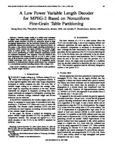
Logic Boards
of pins
Net X
I I I I
I I I I
I I I I
I I I I
Paths to next level of interconnect
Chips
I I 9w’+c*cP I I Connectionsto Other Cardcages
Fig. 1. Partial crossbar interconnect. Fig. 2. Second-level partial crossbar.
Interconnect Architecture Previous logic emulators [4] connected M A ’ s in a twodimensional array. Each FPGA in that emulator has two jobs: logic and interconnection. Many pins are used up by nets passing through an FPGA but not connecting to its logic. Fewer pins are available for logic and low FPGA utilization results. In addition, overall net delays vary widely, since some nets may pass through many FPGA’s from end-to-end. This variation not only slows down the network, but also introduces hold time violations which prevent correct operation unless compensated for. Another disadvantage of this approach is that placement becomes a nontrivial problem and makes the software architecture much more complex. Logic and interconnection are separated in the Realizer architecture. FPGA’s which emulate logic are not connected to each other and are served by a circuit-switched interconnect. All logic FPGA pins are used for connections to intemal logic permitting maximum utilization. The ideal circuit-switched interconnect would be economical, reliable in that it succeeds in interconnecting all designs, scale in size directly with logic size, and has small and bounded propagation delay. A full crossbar is ideally reliable, with fast and bounded delay, but its size grows as the square of its pin count and so is not economical [5]. However, a logic emulator does not need its full generality. FPGAs offer an additional degree of freedom in that they can be configured to use any of their U 0 pins for any given net. This freedom is critical to the viability of the partial crossbar interconnect.
Partial Crossbar Interconnecr The partial crossbar interconnect (Fig. I ) consists of a set of small full crossbars, connected to logic FPGA’s but not to each other. The 110 pins of each logic FPGA are divided into proper subsets, using the same division on each one. The pins of each crossbar chip are connected to the same subset of pins from each logic chip. Thus crossbar chip I I is connected to subset I I of each logic chip’s pins. As many crossbar chips are used as there are subsets, and each crossbar chip has as many pins as the number of pins in the subset times the number of logic chips. Each logic chipkrossbar chip pair is interconnected by as many wires, called paths, as there are pins in each subset. The partial crossbar’s size increases linearly with the total number of logic chip pins. This, in tum, is directly related to the number of logic chips and thus logic capacity, which is the desired result. It is fast, in that all interconnections pass through only one crossbar chip. It is relatively easy to use and, since it is regular, its paths can be represented in a table and determining how to interconnect a particular cut net is simply a matter of searching that table for the best available set of paths. Partial crossbars can be applied recursively to interconnect large systems, as shown in Fig. 2. In addition to the pins that connect to logic chips on the same board, each crossbar chip has additional pins that go off-board. Multiple boards can be interconnected by a second-
level set of crossbar chips; multiple cardcages can be interconnected by yet another level of crossbar chips, and so on. Using multilevel partial crossbars introduces a modest placement task to minimize the number of nets which must traverse multiple levels. Very large systems may be interconnected with little delay. The path from gate to gate on one board goes through at most one crossbar chip. Three crossbar chips connect any gate on one board to any gate on another board, and the path across cardcages goes through five chips. This delay uniformity minimizes the number and degree of setup and hold time violations introduced by the emulator.
Capability of the Partial Crossbar A partial crossbar interconnect cannot handle quite as many nets as a full crossbar serving all pins could. There may be situations where there is no way to interconnect a net even though there are free pins on the relevant logic and interconnect chips. This happens less frequently when fewer crossbar chips with more pins each are used, since the number of pins per subset increases. However, larger crossbar chips are more expensive. The need to quantify the effectiveness of partial crossbar interconnect configurations motivated the following study. To compare the partial crossbar’s ability to interconnect networks with that of a full crossbar, a special program generates a random synthetic network that fully saturates all logic chip pins with a collection of nets. The number of pins per net is according to a predefined distribution representative of logic design networks. Various net pincount distributions and partial crossbar configurations were modeled. One hundred networks were generated and interconnected for each configuration. The results for the case with 33% 2-pin, 38% 3-pin, 19% 4-pin, and 10% 5-pin nets are shown in Table I. The final three columns show the number of nets in the generated saturating network, the number connectable by the partial crossbar, and the ratio of those two. A full crossbar would succeed for 100% of the nets. These results indicate that a narrow partial crossbar is nearly as effective as a wide one or even a full crossbar. By providing a small additional margin of logic chip pins and crossbar chips, we find that logic designs are nearly always interconnectable by a narrow partial crossbar. Across many actual design cases, a failure to connect all nets has yet to be observed. 111. SOFTWARE ARCHITECTURE
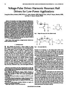
The Realizer software system consists of the configuration system and the run-time system. The configuration system is depicted in Fig. 3. It takes a design file as input, and creates a configuration file as output; these are used by the run-time system to configure and use the Realizer hardware. The design reader reads in the design file and creates data structures that correspond to the primitives and nets in the design. Since the primitives in the input may not correspond to those available in the FPGA, some form of primitive conversion
IEEE TRANSACTIONS ON VERY LARGE SCALE INTEGRATION (VLSI) SYSTEMS, VOL. I , NO. 2, JUNE 1993
Logic Chips boardper
I
Crossbars
Pins per chip
Chips per board
I
Nets connected (avg.)
% nets
connected
step is a configuration bit file for each chip. These are collected by the configuration file collector, which creates a single configuration file. The Realizer run-time software uses the configuration file to program each chip in the hardware system. Once a design has been downloaded, it is ready for emulation; bit vectors can be used to stimulate the design inputs and samplers on the design outputs can be used to observe the behavior of the system. The Realizer run-time system provides an S-window interface to the hardware so that it can be accessed as a network resource.
Primitive Converter Partitioner
Nets generated (avg.)
Pins per
Pins per chip
Design Reader
I
I73
I
IV. RESULTS
m1$m l el Conversion Conversion Conversion Conversion
A A A A
ConfigurationFiles for Each Lo~icand Interconnect Chip
“
Y
Y
Y File
Fig. 3. Realizer software system. must be performed. Some optimization is also performed to remove primitives and nets that do not affect the outputs of the design thereby helping to decrease its logic requirements. After a design has been converted, it is partitioned into FPGAsized bins. The goal of the partitioner is to minimize the number of cut nets that result from the partitioning. Minimizing cut nets is important because FPGA’s tend to be pin-limited. The partitioning is hierarchical because there are different constraints at different levels of the interconnect hierarchy and they must all be simultaneously satisfied. Placement of the FFGA-sized bins is fairly easy since the interconnect is so symmetric. Once a design has been partitioned, it must be interconnected in order to retain the connectivity of the original design. Interconnection is accomplished by picking a set number for each cut net. The set determines which subset of pins on a logic chip are used as well as which interconnect chip connects these logic chip pins. Once all the cut nets have been assigned a set, pin assignments can be chosen for each logic and interconnect chip. At this point each of these chips has all the information it needs to be placed and routed. The design is then written out as a collection of netlist files, one for each chip. Each chip can be independently placed and routed using the software provided by the FPGA vendor. The result of the chip place and route
An actual Realizer system has been built and operated.The system’s logic board has 14 Xilinx XC3090-70 logic FPGA’s [3], with 128 pins each used for interconnect, and 32 Xilinx XC2018-100 FPGAs used as crossbar chips. These 32 subsets have 4 pins each. In addition, 16 pins from each crossbar chip go off-board, totaling 5 12. A secondlevel crossbar of 64 XC2018-100 chips, interconnects up to 8 logic boards, of which 3 have been built. The Realizer has emulated many actual designs (Table 11); the gate utilizations are substantially better than those shown by previous emulators. A commercial product called the Enterprise Emulation System [6] manufactured by Quicktum Systems is a more advanced embodiment of the ideas presented here. It also uses the partial crossbar interconnection scheme. A complete system is capable of emulating up to 330K gates and is composed of 1 I Emulation Modules (EM’S). Each EM has 46 Xilinx FPGA’s and 46 fill custom interconnection chips. Each logic chip has 138 pins that are organized as 46 subsets with 3 pins each. There are 1380 pins coming out of each EM connecting to the second-level interconnect which has I44 interconnection chips. In addition, a third level of interconnect can be used to connect multiple Enterprise systems to provide multimillion gate emulators. The Enterprise system has configured and emulated dozens of designs [7] and some of the results are presented in Table 111.
v.
APPLICATIONS AND FURTHER WORK
Currently logic emulators are used to prototype logic designs, for real-time verification and operation [4]. They are also used with stimuluskesponse vector memories as very high-speed simulation accelerators, modeling without delay and with two or three logic states. A number of researchers have built arrays which are similar to logic emulators for use as reconfigurable accelerators [8], [9]. In these applications, the partial crossbar architecture improves FPGA utilization, allowing larger logic capacity for a given amount of hardware, and its bounded delay characteristics provide more reliable implementation. An application worthy of further development is the use of a logic emulator as a workbench for experimental architectures. An architecture may be implemented and tested on real applications in a short time, then modified and retested without building any hardware. The flexibility and reusability of an emulator allows more
I
174
IEEE TRANSACTIONS ON VERY LARGE SCALE INTEGRATION (VLSI) SYSTEMS, VOL. I , NO. 2, JUNE 1993
TABLE I1 REALIZER RESULTS
Design
DesiRn size (gates) 3K 7K 17K 35K
1
2 3 4
Number of chips 3 12 16 28
Gates per chip IO00 583 1037 I257
Notes Register file RISC CPU datapath Communications controller Array of multipliers
TABLE I11 ENTERPRISE SYSTEM RESULTS
No. of emulation
Design
Design size (gates)
No. of chips
Gates per chip
I
48K 66K 87K
42 121 I62
1 I42
I
545 537
3 3
2 3
architectures to be implemented and experimented within a shorter time span than is possible when chip fabrication is required. A Realizer logic emulation system with memory and arithmetic functional units as well as logic FPGA’s may be configured to execute a variety of computing functions. Applications include DSP, pattem matching, data compression, visualization, neural networks and fast format translation.
REFERENCES M. Butts and J. Batcheller, “Method of using electronically reconfigurable logic circuits,” U.S. Patent 5 036 473, July 30, 1991. M. Butts, J. Batcheller and J. Varghese, “An efficient logic emulation system,” in Proc. fnt. Con$ on Computer Design, pp. 138-141, Oct. 1992.
modules
Notes Register file CPU interface buffer
[3] Xilinx, Inc., The Programmable Gate Array Dura Book, Xilinx, San Jose, 1992. [41 S. Walters, “Computer-aided prototyping for ASIC-based systems,’’ IEEE Design & Test, pp. 4- IO, June 1991. 151 G. Masson, G. Gingher, and S. Nakamura, “A sampler of circuit switching networks,” IEEE Computer, pp. 32-48, June 1979. [61 L. Maliniak, “Multiplexing enhances hardware emulation,” Electronic Design, pp. 76-78, Nov. 1992. [7] M. Butts, J. Batcheller, and M. Heising, “Programmable interconnect for logic emulation,” Quicktum Systems, Oct. 1992, (in review). [81 C. Cox and W. Blanz, “Ganglion-A fast hardware implementation of a connectionist classifier,” in P roc. fEEE Custom Integrated Circuits Con&, 1991. [9] M. Shand, P. Bertin, and J. Vuillemin, “Hardware speedups in long integer multiplication,” ACM Computer Architecture News,pp. 106- I 13, Mar. 1991.