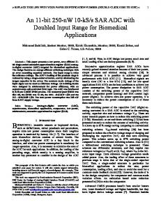
An Ultra-Low-Power SAR ADC with an Area-Efficient DAC Architecture Pouya Kamalinejad, Shahriar Mirabbasi, and Victor C.M. Leung University of British Columbia, Department of Electrical and Computer Engineering, Vancouver, BC, Canada, V6T 1Z4
[email protected],
[email protected],
[email protected]
Abstract—An ultra-low-power area-efficient 8-bit successive approximation register (SAR) analog-to-digital converter (ADC) is presented. To achieve ultra-low-power performance a DAC architecture is proposed that employs two rail-to-rail low-power unity-gain buffers and only 4 minimum-size capacitors instead of the conventional binary-weighted capacitor array. Thereby, power consumption and area are drastically reduced by virtue of lower switching activity and smaller size capacitor array. The proposed 8-bit SAR ADC is designed and simulated in a 0.13µm CMOS process. Simulation results show that for a 2.4 kHz (12.4 kHz) input signal while sampling at 25 kHz, the ADC achieves an ENOB of 7.9 (7.8), consumes 290 nW (350 nW) form a 0.8 V analog supply and a 0.6 V digital supply, and achieves a FoM of 48 fJ/conversion-step (62 fJ/conversion-step).
I. I NTRODUCTION Emerging mixed-signal applications such as radio-frequency identification (RFID) systems, wireless sensor networks, portable biometric devices and energy scavenging systems demand a high power efficiency to secure a long autonomous operation. Analog-to-digital converters (ADCs) are among critical components that are used in most of such systems and usually consume a fair share of the overall power budget. Among different ADC architectures, successive approximation register (SAR) ADCs [1-6] are the most popular candidate for the aforementioned applications which typically require highresolution, low-to-medium speed and low power. Conventional SAR ADCs use the standard binary search technique [1-6]. Generally, in a SAR ADC there are two major contributors to power consumption: comparator and charging/discharging of the DAC array. However, comparator’s power consumption is usually not a matter of concern unless a very high-speed and high resolution is required. (Yet, a comparator architecture compatible with the proposed digitalto-analog converter (DAC) structure is briefly discussed in the paper.) Typical SAR structures use bulky DAC capacitive arrays which are usually the area and power bottleneck of the design. From the power dissipation perspective, in order to sample a full-scale sine wave at the Nyquist frequency, a traditional capacitive array on average consumes [7]: Pin =
CT VR2 Ts
(1)
This research is funded in part by the Natural Sciences and Engineering Research Council of Canada (NSERC) and the Institute for Computing, Information and Cognitive Systems (ICICS) at UBC. CAD support and access to technology is facilitated by CMC Microsystems.
978-1-4244-9474-3/11/$26.00 ©2011 IEEE
13
where Pin is the power drawn from the input, CT is the total capacitance of the array, VR is the reference voltage and Ts is the conversion period. The average power drawn form the reference generator for charge redistribution is [7] : Pref =
CT VR2 2Ts
(2)
Accordingly, layout area and power consumption grow exponentially (CT = 2n C0 ) with the number of bits (n) which compromises the advantage of SAR ADCs in terms of area and power, especially as the number of bits increases. Extensive studies have been carried out on energy-efficient DAC structures [1-8]. [2] proposes the capacitor splitting scheme which reduces the average switching energy of the array by splitting the most significant bit (MSB) capacitor into n − 1 binary scaled sub-capacitors (where n is the number of bits). Consequently, for down transitions [2], the charge on the MSB capacitor will be restored for further conversions. Although the proposed technique significantly saves the switching energy for small output codes, it fails to perform equally well for higher output codes where less down transitions occur. Moreover, this approach is still dependant on a bulky DAC array and requires twice as many switches as the conventional scheme. In another structure, [8] reduces the average switching energy of the capacitive array by separating the decoding of MSB and least significant bit (LSB) through using two different capacitor arrays with unequal size. However, the lowpower consumption is achieved at the cost of two additional clock cycles which poses energy overhead due to additional comparison steps required. Moreover, the layout occupies a higher area than that of the traditional architecture due to MSB DAC, memory storage with logic and the extra comparator. This paper proposes an area-efficient DAC architecture that both reduces the power consumption and the layout area. The proposed DAC architecture consists of four minimum-size capacitors and two low-power buffers for which the binary search algorithm is carried out at no extra cost in terms of clock cycles and comparison steps. Also, the use of four minimum-sized capacitor DAC relaxes capacitor mismatch and parasitic requirements. To further save area and power consumption, the two low-power buffers are dually used as the comparator preamplifier blocks in an open-loop fashion. Section II presents the DAC architecture while Section III describes the proposed comparator. In Section IV, the sample-
VREF
VREF
Ctop1
Ctop2
S3
S5
S1 St1
VTOP1 VMID1
VTOP2 B1
Sb1 Conventional SAR architecture
Sb2
B2
S2
VBOT2 S6
S4
Cbot1
and-hold architecture is described, and Section V provides the simulation results.
VTOP1
VREF
The operating principles of a SAR converter are well known [1-7] . Simply put, the capacitive DAC main task is to provide the appropriate voltage levels to implement the binary search algorithm as shown in Fig. 1. The algorithm starts by setting the MSB to ’1’ and all other bits to ’0’. Thereby, Vin is compared with V2ref . Charge recycling is then carried out based on the output of the comparator, i.e., if D1 (comparator output) is high, the second largest capacitor is charged to Vref setting VDAC = 3V4ref . This is called an ”up” transition. Conversely, if D1 is low, the largest capacitor is discharged and the second largest one is charged to Vref which is called a ”down” transition. The sequence continues until all the bits are decided. The binary search algorithm described above can be interpreted as follows: two voltage levels are defined as Vtop and Vbot which are the upper and lower voltage bounds at each clock cycle and they converge toward Vin with each bit decision. Vmid is then produced from Vtop and Vbot as:
down transition VTOP2
down transition
VMID2
VTOP1
VBOT1
VBOT2
VBOT1
Bit1=0
Bit2=0
Bit3=1
Vmid =
Vtop + Vbot 2
(3)
For the mth bit, this voltage, i.e., the output of the DAC, is compared with Vin and the comparison result Dm updates the value of Vtop or Vbot in the next clock cycle such that if Dm = 1 (’up’ transition), Vtop maintains its old value while Vbot is shifted up to Vmid . Conversely, if Dm = 0 (’down’ transition), Vbot retains the old value and Vtop is shifted down to Vmid . The procedure continues until all bits are concluded. As shown in Fig. 2 the algorithm can be implemented using four capacitors and two unity gain buffers. For a given output of ’001...’ (where the first three bits are evaluated) the operation of the proposed DAC architecture can be described as follows: Each bit decision cycle is divided into two time slots, comparison cycle and charge recycling cycle. During each comparison cycle one capacitor set (Ctopi , Cboti ) performs as a capacitive V +V divider producing Vmid = top 2 bot and the other set holds the same two voltage levels (Vtop , Vbot ) that are being processed (the two capacitor sets interchangeably switch these two tasks in subsequent comparison cycles). Voltage levels are then updated at charge recycling cycle based on the previous decision. At the beginning of conversion (sampling phase), (S1 , S7 ) and (S2 , S8 ) are on, charging (Ctop1 , Ctop2 ) and (Cbot1 , Cbot2 ) to VREF
14
VIN
VMID1
VGND
Fig. 2.
S8
Cbot2
II. DAC A RCHITECTURE VMID1
St2
VMID2
VBOT1 Fig. 1.
S7
VTOP2 VBOT2
up transition
New DAC architecture and timing diagram.
and VGND , respectively. Then in the first comparison cycle, (S1 , S2 ) and (S7 , S8 ) turn off and (St1 , Sb1 ) turn on to form a capacitive divider (from Ctop1 , Cbot1 ) which gives VMID1 = V2REf . Note that as stated earlier when each capacitor set is active, i.e., providing VMID for comparison (Ctop1 , Cbot1 ), it is essential that the other capacitor set (Ctop2 , Cbot2 ) holds the same voltage levels being searched at the time, which in this case is VTOP2 = VREF and VBOT2 = 0. Then VMID1 is compared with VIN which yields D1 = 0 based on the assumption made for the first three bits. Voltage levels are updated in the succeeding charge recycling cycle. As mentioned earlier for each ’down’ transition Vbot maintains its value and Vtop is shifted down to VMID . For this purpose, (St1 , Sb2 ) and (S4 , S5 ) are switched on while all other switches are off. Buffer B1 provides a copy of VMID1 for Ctop2 thus shifting Vtop2 down to VMID1 . At the same time, buffer B2 returns Cbot1 voltage back to VBOT1 = VGND in order for (Ctop1 , Cbot1 ) to have a copy of new voltage levels that are to be processed in the next comparison cycle. At this point, Vtop1 = Vtop2 = VREF and Vbot1 = Vbot2 = 0 and the 2 capacitors are all set for the next comparison cycle where (St2 , Sb2 ) turn on and all other switches are off. The capacitive BOT2 divider produces VMID2 = VTOP2 +V = VREF 2 4 . This voltage is compared with Vin and results in D2 = 0 which corresponds to a ’down’ transition. In the next charge recycling cycle, (St2 , Sb1 ) and (S3 , S6 ) are switched on. Buffer B2 shifts VTOP1 down to VMID2 = VREF 4 and buffer B1 returns VBOT2 back to VGND such that Vtop1 = Vtop2 = VREF and Vbot1 = Vbot2 = 0. Therefore, 4 in the next comparison (Ctop1 , Cbot1 ) produce VMID1 = VREF 8 which yields D3 = 1. In the next charge recycling cycle (St2 , Sb1 ) and (S3 , S6 ) are switched on. Buffer B1 pulls VBOT2 up VREF to VMID1 = VREF 4 and buffer B2 returns VTOP1 back to 2 . All the next bits are decided in the same manner. In terms of power, the proposed architecture outperforms
VREF
VREF
CLKcomp OUT+
CLKcomp
VIN VMID1 VMID2
CLKcomp1
CLK-latch
Mp1
OUT-
OUT+
B1
Mp2
OUT+
OUT
CLK-pre CLKcomp2
CLKcomp2 CLKcomp1
OUT-
B2
CLKcomp
VMID2 VMID1 VIN
CLKcomp
CLK-latch CLK-pre
CLK-latch
OUT-
CLK- pre
CLKcomp
Fig. 3.
OUT
SL
CLKcomp1,2
Mn1
CLK-latch
Mn2
CLK- off
Proposed comparator architecture and timing diagram.
Fig. 4.
Low-power latch architecture. VREF
the conventional SAR architectures. As the algorithm suggests, during a conversion cycle, each of the two buffers contribute in the charge recycling process for at most n times. So, the total charge drawn from VREF during the conversion cycle is: Qtot = 4 · n · Ib · TCR
OUT
IB VIN-
VIN+
CC
(4) CLK- off
where n is the number of bits, Ib is the bias current for each buffer stage, TCR is the charge recycling period and the factor ’4’ accounts for the two, two-stage amplifiers. the two factors governing Ib are the required voltage gain and speed. To achieve the desired resolution, the buffer output has to settle within 12 LSB of the input, which for an 8-bit resolution requires an open loop gain on the order of 50 to 60 dB. The two-stage low-power amplifier (described in Section III) provides such a gain by drawing only 124 nW from VREF . Regarding speed, since the load capacitance is minimum-sized, slew-rate is not that critical and charge-recycling period (TCR ) can be very short. The aforementioned algorithm is implemented in the proposed ADC with some minor amendments. To further save power, the buffers turn off whenever their service is not required. This is achieved by shutting off the supply current (the buffer architecture is described in Section III ). An example for such a power saving mode is when the destination voltage, VTOP or VBOT is supposed to be updated to VREF or VGND , respectively. In this situation the respective buffer will not perform the task, instead one of (S1 , S7 ) or (S2 , S8 ) turns on to update VTOP or VBOT to VREF or VGND , respectively. This power saving scheme proves useful particularly for very large or very small inputs. For instance, for a very small output code starting with several consecutive ’0’s (0000...), at each charge recycling cycle, one buffer remains inactive until the first ’1’ is detected. The same goes for very large output codes. III. C OMPARATOR A RCHITECTURE As mentioned in Section I, to further save area and power, the two buffers employed in DAC are used as the preamplifier stages for the comparator by opening the loop through CLKcomp , as shown in Fig. 3. At each comparison phase, one capacitor set provides VMID to be compared with VIN for which
15
Sb2 Sb1 CLK- off
Fig. 5.
Low-power amplifier.
the appropriate clock (CLKcomp1 or CLKcomp2 ) goes high. To better utilize the available hardware, the two amplifiers operate simultaneously to amplify the voltage difference between the input voltages. For this purpose VIN and VMIDi are applied to opposite terminals of B1 and B2 . Thus, as one of OUT+/OUTcharges up to VREF , the other one is pulled down to VGND . This scheme brings a twofold benefit: on the one hand, the pre-amplification phase would be twice as fast. On the other hand the overall comparator resolution is improved. Almost at the end of comparison cycle where OUT+ and OUT- are about their extreme voltage levels (note that clock periods are not drawn to scale in Fig. 3), a very short pulse CLKpre , connects OUT+ and OUT- to the input terminals of the regenerative latch as shown in Fig. 4. CLKpre turns off after a short period so that B1 and B2 do not drive the latch for the rest of the latch cycle. The buffer/amplifier architecture is shown in Fig. 5. After the pre-amplified voltages are properly delivered to the latch at the end of CLKpre , CLKoff goes high which turns the amplifiers off by shutting off the bias currents through Sb1,2 . Latch phase starts simultaneously with CLKpre and the regenerative latch produces a digital level output in a very short interval. At the end of process, SL resets the latch by connecting the input and output of the back-to-back inverters to set them close to VREF which speeds up the next latch 2 operation. To further save power, Mn1,2 and Mp1,2 perform the power-gating task by blocking the latch input current in inactive mode when CLKlatch is off.
VREF CLKH
CLKH
Crefresh CLKH
CLKH
Cboost CLKSAMPLE
MH2
Sampling Period
MS2
-VREF
V
G S
VGS
Msample
Simulated DNL and INL at 25kS/s.
VREF
MS1 CLKSAMPLE
VIN
Fig. 7.
CLKSAMPLE
MH1
Mdummy
Csample
CLKSAMPLE
Fig. 6.
Proposed Sample-and-Hold architecture and timing diagram. Fig. 8.
IV. S AMPLE AND H OLD A RCHITECTURE A switched-capacitor clock-boosted architecture is used for the sample-and-hold circuit due to its rail-to-rail capability and low-power operation. As shown in Fig. 6, after a few clock periods, Cboost is charged to VREF and subsequently acts as a floating voltage source. At each sampling phase (CLKSAMPLE ), Cboost connects the gate-source terminals of Msample in such a way that: VGS = VREF . Therefore in sampling phase, the gate voltage of Msample will always be as much as VREF higher than its source voltage, regardless of the value of VIN . This presents a rail-to-rail operation. On the other hand, in the hold phase, MH1 , MH2 turn on and MS1 , MS2 turn off, providing a negative voltage between the gate-source terminals of Msample such that for the entire hold phase: VGS = −VREF . This negative bias alleviates the leakage current and fully isolates the sampled voltage from input fluctuations. CLKH can be picked from any of the clock signals already generated in the circuit, however, for a better performance, it has to be a high frequency clock such as CLKcomp . As shown in Fig. 6, Crefresh updates the voltage on Cboost at every CLKH . Mdummy is employed to cancel the charge-injection effect. However, special care has to be given to the size of Mdummy SizeMSample which is not the conventional due to the fact that the 2 gate-source voltages that the two transistors experience are not the same. Note that this architecture almost imposes no power consumption penalty as the current drawn from VREF is limited to the leakage current of Cboost and switching transistors and thus is on the order of few nano Watts. V. S IMULATION R ESULTS The proposed DAC/comparator architecture is designed and laid out in an 8-bit 25kS/s SAR ADC in a 0.13µm CMOS technology. DAC capacitors are implemented by a MIM structure with the unit capacitor of 50 fF and the sampling capacitor is 500 fF. As shown in Fig. 7, at 25kS/s the simulated DNL and INL are within 0.25 LSB and 0.5 LSB, respectively. The spectra for an input full-scale sine wave at 2.24 kHz and 12.4 kHz are shown in Fig. 8, for which the SNDRs of 49.4 dB (ENOB=7.91) and 48.8 dB (ENOB=7.81) are obtained, respectively.
16
Output spectrums for input sine wave @ 2.24kHz and 12.4kHz.
The entire digital circuitry is custom designed and dissipates 24 nW from a 0.6 V supply. The total power consumption for 2.24 kHz and 12.4 kHz input sine-wave are simulated to be 290 nW and 350 nW which exhibits a FoM of 48 fJ/conversion-step and 62 fJ/conversion-step, respectively. A comparison of the proposed architecture with the state-ofthe-art SAR ADCs is provided in Table I. TABLE I C OMPARISON OF THE P ROPOSED SAR ADC S TATE - OF - THE -A RT R ESULTS [1]? [3]? [4]? Technology (µm) 0.18 0.18 0.13 Supply Voltage (V) 1 (1) 0.9 1.2 Sampling Rate, fs (kS/s) 200 (100) 200 1000 Input Frequency, fin (kHz) 100 (50) 100 101 ENOB (@fin ) 7.96 (10.55) 7.44 8.39 Power Dissipation (µW) 19 (25) 2.47 150 FoM† (fJ/conversion-step) 381 (166) 65 437‡
WITH THE
[5]?? 0.13 1 100 48.5 9.17 1 17
This work?? 0.13 A: 0.8, D: 0.6 25 12.4 7.81 0.35 62
?Measurement results. ?? Simulation results. † FoM = Pdiss /(2 · fin · 2ENOB ) ‡ FoM = Pdiss /(fs · 2ENOB )
R EFERENCES [1] N. Verma and A. Chandrakasan, “An ultra low energy 12-bit rateresolution scalable SAR ADC for wireless sensor nodes,” IEEE Journal of Solid-State Circuits, vol. 42, no. 6, pp. 1196 –1205, Jun. 2007. [2] B. Ginsburg and A. Chandrakasan, “An energy-efficient charge recycling approach for a SAR converter with capacitive DAC,” IEEE International Symposium on Circuits and Systems (ISCAS), pp. 184 – 187, May. 2005. [3] H.-C. Hong and G.-M. Lee, “A 65-fJ/conversion-step 0.9-v 200-kS/s railto-rail 8-bit successive approximation ADC,” IEEE Journal of Solid-State Circuits, vol. 42, no. 10, pp. 2161 –2168, 2007. [4] Z. Zeng, C.-S. Dong, and X. Tan, “A 10-bit 1MS/s low power SAR ADC for RSSI application,” IEEE International Conference on Solid-State and Integrated Circuit Technology (ICSICT), pp. 569 –571, Nov. 2010. [5] R. Lotfi, R. Majidi, M. Maymandi-Nejad, and W. Serdijn, “An ultra-lowpower 10-bit 100-ks/s successive-approximation analog-to-digital converter,” IEEE International Symposium on Circuits and Systems (ISCAS), pp. 1117 –1120, May 2009. [6] M. Scott, B. Boser, and K. Pister, “An ultralow-energy ADC for smart dust,” IEEE Journal of Solid-State Circuits, vol. 38, no. 7, pp. 1123 – 1129, Jul. 2003. [7] A. Agnes, E. Bonizzoni, and F. Maloberti, “Design of an ultra-low power SA-ADC with medium/high resolution and speed,” IEEE International Symposium on Circuits and Systems (ISCAS), pp. 1 –4, May. 2008. [8] R.-k. Choi and C. ying Tsui, “A low energy two-step successive approximation algorithm for ADC design,” IEEE International Symposium on Circuits and Systems (ISCAS), pp. 17 –20, May. 2009.