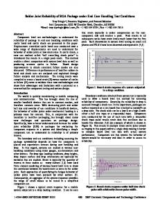
Ball Grid Array (BGA) Solder Joint Intermittency Detection: SJ BIST James P. Hofmeister Ridgetop Group, Inc. 6595 N. Oracle Rd. Tucson, AZ 85750 (520) 742-3300
[email protected]
Pradeep Lall Dhananjay Panchagade Auburn University Dept. of Mech. Engineering and CAVE Auburn, AL 36849 (334) 844-3424
[email protected] [email protected]
Terry A. Tracy Raytheon Missile Systems Bldg. M02, MS T15 1151 Hermans Road Tucson, AZ 85706-1151 (520) 794-3962
[email protected]
Justin B. Judkins Kenneth L. Harris Ridgetop Group, Inc. 6595 N. Oracle Rd. Tucson, AZ 85750 (520) 742-3300
[email protected] [email protected]
Abstract—This paper presents test results and specifications for SJ BIST™, an innovative sensing method for detecting faults in solder-joint networks that belong to the I/O ports of Field Programmable Gate Arrays (FPGAs), especially in Ball Grid Array packages. It is well-known that fractured solder joints typically maintain sufficient electrical contact to operate correctly for long periods of time. Subsequently the damaged joint begins to exhibit intermittent failures: the faces of a fracture separate during periods of stress, causing incorrect FPGA signals. SJ BIST detects faults of 100 Ω or lower with zero false alarms: minimum detectable fault period is one-half the period of the FPGA clock; guaranteed detection is two clock periods. Being able to detect solder joint faults in FPGAs increases fault coverage and health management capabilities, and provides support for condition-based and reliability-centered maintenance12.
1. INTRODUCTION This paper presents test results and specifications for SJ BIST™ (Solder Joint Built-in-Self-Test™), which is an innovative sensing method for detecting faults in solder-joint networks that belong to the I/O ports of Field Programmable Gate Arrays (FPGAs), especially FPGAs in Ball Grid Array (BGA) packages such as a XILINX® FG1156 [1-6]. FPGAs are widely used as controllers in aerospace applications, and being able to detect faults in solder-joint networks increases both fault coverage and health management capabilities and support for condition-based and reliability-centered maintenance. As both the pitch between the solder balls of the solder joints of BGA packages and the diameter of the solder balls decrease, the importance a real-time solder-joint fault sensor for FPGAs increases. SJ BIST is the first known for detecting highresistance faults in solder joint networks of operational FPGAs.
TABLE OF CONTENTS 1. 2. 3. 4. 5. 6. 7. 8. 9. 10.
INTRODUCTION .................................................1 SJ BIST .............................................................4 INTERMITTENCY MITIGATION .........................5 PIN SELECTION .................................................6 TEST ACTIVITIES ..............................................6 DEMONSTRATION BOX......................................8 SUMMARY AND CONCLUSION ...........................8 ACKNOWLEDGEMENT .......................................9 REFERENCES .....................................................9 BIOGRAPHY .................................................10
The current version of SJ BIST is a Verilog-based, two-pin test group core to be incorporated within an end-use application in the FPGA. Test assemblies of printed wire (circuit) boards (PWBs) with programmed FPGAs have been assembled and are being tested to failure at the Center for Advanced Vehicle Electronics (CAVE) at Auburn University; in Germany under the sponsorship of an automobile manufacturer, and at Ridgetop Group facility in Tucson, Arizona. Raytheon Missile Systems, Tucson, has acquired demonstration boxes for both evaluation and for testing.
1 1 2
Norman N. Roth DaimlerChrysler AG Cabin/Power Train E/E 050/G009-BB GR/EEH 71059 Sindelfingen, Germany 49-(0) 7031-4389-398
[email protected]
SJ BIST correctly detects and reports instances of highresistance with no false alarms: test results are shown in this
1-4244-1488-1/08/$25.00 ©2008 IEEE. IEEEAC paper #1148, Version 8, Updated 2007:10:23.
1
BGA Package
paper. The program for the test boards contains temporary data collection routines for statistical analysis and uses less than 250 cells out of over 78,000 cells for a 5-million gate, 1156-pin FPGA to test 8 pins.
Contact Pad Solder Ball PCB Land
Crack Layer 1
Initial testing indicates SJ BIST is capable of detecting highresistance faults of 100 Ω or lower and which last one-half of a clock period or longer. In addition to producing no false alarms in the current period of testing, no additional failure mechanisms are introduced to an assembly because, with the exception of fault reporting and handling, SJ BIST is (1) not invasive to an application program; (2) is not compute intensive and so timing problems are not anticipated; and (3) any failures in SJ BIST itself is a failure in the FPGA or the board. Therefore either a real failure is reported or no failure is reported and neither is a false alarm.
Multi-Layer PCB
Layer 2
Dielectric
Layer 3 00056
Figure 3: Crack at Solder Ball-PCB Junction. BGA Package Contact Pad
Fracture
PCB Land
Solder Ball Layer 1
Multi-Layer PCB
Layer 2
Dielectric
Layer 3
Mechanics of Failure
Failure Point: Fracture of the Solder Ball
Solder-joint fatigue damage caused by thermo-mechanical and shock stresses is cumulative and manifests as voids and cracks, which propagate in number and size. Eventually, the solder ball (or bump) of the joint fractures [7-10] and FGPA operational failures occur. An illustration of a damaged solder bump on the verge of fracturing is shown in Figure 1.
00017
Figure 4: Fractured Solder Ball. Intermittent Behavior of Fractured Solder Bumps Over time, contamination and/or oxidation films form on the fractured surfaces and a failure progression occurs: from degraded joints to intermittent opens of short duration (nanoseconds or less) to longer durations (microseconds) to very long durations lasting milliseconds or longer. The latter case, with intermittent faults lasting milliseconds or longer, are very likely to cause faults in the correct FPGA operation. Test results confirm this physics of failure behavior. As seen in Figure 5, during periods of high stress, fractured bumps tend to momentarily open and cause hard-to-diagnose, intermittent faults of high resistance of 100s of Ohms [1012]. Such faults typically last for periods of hundreds of nanoseconds, or less, to more than 1 µs [7, 11, 13-16]. The intermittent faults are caused by the opening and closing of the fractured faces of the solder balls, as depicted in Figure 6.
Figure 1: Cracked Solder Ball (Bump), 15mm BGA [8]. Figure 2 and Figure 3 depict a cracked solder ball of a BGA package attached to an electronic printed circuit board (PCB); Figure 4 depicts a fractured solder ball, which is what happens to a crack as an end result of accumulated fatigue damage. A fracture is the complete separation of a solder ball that can result in a break in the electrical connection between the BGA and the electronic board. BGA Package Crack
Contact Pad PCB Land
Solder Ball Layer 1
Multi-Layer PCB
Layer 2
Dielectric
Layer 3 00055
Figure 5: Shock-actuated Failure: Transient Strain (Blue) and Intermittent Opens (Mauve) (From Lall).
Figure 2: Crack at BLM and Solder Ball.
2
These intermittent faults increase in frequency as evidenced by a practice of logging BGA package failures only after multiple events of high-resistance: an initial event followed by some number (for example, 2 to 10) of additional events within a specified period of time, such as ten percent of the number of cycles of the initial event [14-16]. Even then, an intermittent fault in a solder-joint network might not result in an operational fault. For example, the fault might be in a redundant ground or power connection; or it might occur during a period when the network is not being written; or it might be too short in duration to cause a signal error. In Figure 5, the duration of the fault in the 5th cycle of stress is over 3 milliseconds. Vibration flexes components, intermittently opening and closing the circuit
Figure 8: XILINX FPGA HALT Test Results [15].
BGA Package FPGA
State of the Art
FPGA
The use of leading indicators of failure for prognostic indication of impending failure has been previously demonstrated [17-20]. One important reason for using an in-situ solder-joint fault sensor is that stress magnitudes are hard to derive, much less keep track of [21]; another reason is that even though a particular damaged solder-joint might not result in immediate FPGA operational faults, the fault indicates the FPGA is likely to have, or will soon have, other damaged I/O ports—in short, the FPGA is no longer reliable. In a manufacturing environment, SJ BIST addresses a concern that failure modes caused by the PWBFPGA assembly are not being detected during component qualification [12].
Fracture Solder Ball
PCB Closed Circuit
Open Circuit
00057
Figure 6: Intermittent Open and Closed Connection. Damage accumulates and eventually there is a catastrophic failure, such as might happen when a solder ball becomes displaced as depicted in Figure 7.
FPGAs are not amenable to the measurement techniques typically used in manufacturing reliability tests such as Highly Accelerated Life Tests (HALTs) [10]. This is because, for example, a 4-point probe measurement requires devices to be powered-off; and because FPGA I/O ports are digital, rather than analog, circuits (see Figure 9).
Figure 8 represents Highly Accelerated Life Tests (HALT) results performed on XILINX FG1156 Daisy Chain packages in which 30 out of 32 tested packages failed in a test period consisting of 3108 HALT cycles. Each temperature cycle of the HALT was a transition from -55oC to 125 oC in 30 minutes: 3-minute ramps and 12-minute dwells. What is not immediately apparent is that each of the logged FPGA failures (diamond symbols) represents at least 30 events of high resistance: a FAIL was defined as being at least 2 OPENS within the same temperature cycle. A single OPEN in any temperature cycle was not counted as a FAIL event; and the package was deemed as failed only after 15 FAILS [15] had been logged.
Modern BGA FPGAs have more than a thousand pins and very small pitch and ball sizes, for example, the left side of Figure 10 shows the position of the XILINX FG1156 FPGA die with respect to the FPGA mount, and the right side shows the bottom of the package—a footprint of 35x35 mm2, and an array of 34x34 solder balls. The dense array of fine-pitch and ultra fine-pitch BGA packages with very small pitch and solder ball tends to make physical-, optical-, X-ray- and sonic-based inspection techniques impractical for detecting the onset of damage.
BGA Package Contact Pad Missing Solder Ball
PCB Land
Ridgetop authors physically ground down one of the test boards to create the cut view shown in Figure 11. The cut view shows the FPGA die is connected by either flip-chip collapsed connections or by bonding to a ceramic base. Wire interconnects connect the die to ball limiting metallurgy (BLM), to which solder balls are attached. The FPGA package is then placed over connection lands on the
Layer 1
Multi-Layer PCB
Layer 2
Dielectric
Layer 3 00058
Figure 7: Displaced (Missing) Solder Ball.
3
printed circuit board (PCB) and soldered. Note the presence of voids in the two solder balls on the right-hand side of Figure 11: such voids lead to early onset of solder ball failure.
2. SJ BIST SJ BIST requires the attachment of a small capacitor to two unused I/O ports as near as possible to a corner of the package. Figure 12 is a block diagram of an FPGA containing SJ BIST with a capacitor connected to two I/O pins. FPGA SOLDER BALL
FAULT
SJ BIST
CAPACITOR VOLTAGE
Figure 12: SJ BIST Block Diagram Figure 13 shows the signal for a no-fault condition (A) and a fault condition (B). SJ BIST writes a logical ‘1’ to charge the capacitor and then reads the voltage across the charged capacitor. If the solder-joint network of the I/O port of the FPGA is undamaged, the write causes the capacitor to be fully charged and a logical ‘1’ is read by SJ BIST. When the solder-joint network is damaged, the effective resistance of the SJ network increases, the charging time constant increases, the write fails to sufficiently charge the capacitor, and a logical ‘0’ instead of a logical ‘1’ is read: a fault occurs, is detected by SJ BIST and is reported.
Figure 9: FPGA Diagram, I/O Buffer [22].
Die
(A) Figure 10: FG1156: Size is 35x35 mm2; Pitch: 1.0 mm. Ball: 0.6 mm [23].
(B)
Figure 13: SJ BIST: 1 MHz Capacitor Signal. (A) No Fault; (B) 100 Ω Fault − 0.5 µs x 2.0V Grid.
Figure 11: View Showing FPGA Die to PCB Connection.
4
Test Results
For clock frequencies of one-half or higher of the maximum clock frequency of the FPGA, the capacitance of the I/O port is sufficient – no external capacitance needs to be connected for SJ BIST to correctly detect faults with no alarms. Initial test results indicate a fault resolution of about 600 Ohms at full FPGA clock speed.
Tests have been run at various clock frequencies ranging from 10 KHz to 100 MHz and for varying solder-joint network conditions ranging from no fault to over 100 Ω of fault resistance: All faults of 100 Ω or larger were detected, and there were no false alarms.
SJ BIST Signals and Controls
Referring to Figure 13, voltages on a 1.0 µF capacitor connected to a group of two I/O ports are shown. Figure 13A shows the capacitor voltage when one of the two ports connected to the capacitor has a 1 Ω resistor connected in series with the solder joint: the resistance is not high enough cause a write fault to occur, and SJ BIST correctly did not report a detected fault. Figure 13B shows the capacitor voltage when the resistance is increased to 100 Ω, a write fault occurs. SJ BIST correctly reported the fault and incremented the fault count for that I/O pin.
SJ BIST needs to present at least one error signal (a fault indicator) either to an external FPGA I/O port or to an internal fault management program. At least one control signal is required: an enable (disable) BIST. Error Signals and Fault Counts—Each SJ BIST core has two error signals: (1) at least one previous fault has been detected and (2) a fault is currently active. A fault counter (1:255) is also provided. For a deployed SJ BIST, we anticipate most applications would only the first error signal without any count: we use the count for statistical purposes
Clock Frequency, Capacitor Value and Fault Resistance The relationship between the frequency of the FPGA clock, the value of the connected capacitor to each group of two I/O pins, and the detectable fault resistance is shown in Figure 14.
Control Signals— In addition to CLK, SJ BIST has two input signals: ENABLE and RESET. ENABLE is used to turn SJ BIST detection on and off; RESET is used to reset both the fault signal latches and the fault counters. For a deployed SJ BIST, RESET might not be used.
3. INTERMITTENCY MITIGATION SJ BIST is a very useful sensor for mitigating intermittencies. Early detection of failure of an unused I/O pin allows the electronic board to be replaced before subsequent fatigue damage causes an application I/O pin to fail, and therefore intermittent operational anomalies are avoided. Intermittent Behavior of Fractured Solder Joints As previously seen in Figure 5, fractured solder joints tend to maintain electrical contact until periods of increasing stress occur: a hard open longer than a millisecond did not occur until the fifth shock wave. SJ BIST would have recorded at least eight instances of faults: two in each of the first three waves and one each in the fourth and fifth waves Intermittent Confirmation and Prognostic Warning Detection of intermittent faults can be used to confirm that the electronic board with that FPGA is a likely candidate for replacement to address reported operational anomalies. In the absence of any reported operational anomalies, detected faults can be used as a prognostic warning that the board is likely to experience future operational anomalies.
Figure 14: Frequency, Capacitor and Resistance. SJ BIST Sensitivity and Resolution For a given clock frequency, there is a capacitor value that will cause SJ BIST to always detect a fault resistance at least as low as 100 Ω with a duration of at least two clock periods. Faults of shorter duration are detectable when they occur at the beginning of the write and last for about onehalf of a clock period.
5
4. PIN SELECTION Our recommendation is the following: A deployed SJ BIST application should use at least four groups of cores: one group of two I/O pins near each corner of the FPGA die shadow or at each corner of the FPGA package (the pinkshaded pins in Figure 15). Research indicates the solder balls nearest the corner of the package or the FPGA die are most likely to fail first. The stress diagram in Figure 16 indicates that of the two areas, the corners nearest the FPGA die are likely to fail first. High stress caused by physical mounting coupled with thermal-mechanical stresses is the most likely cause of the observed failure distribution of solder balls in BGA packages. Further evidence of the validity of these observations is the reserving of the four I/O pins at each corner for ground and all of the pins under the die for power and ground (the orange-shaded pins).
Figure 16: FG1156 Strain Diagram.
HALT Test Board
5. TEST ACTIVITIES
Figure 17 is a block diagram of the HALT test board we designed. The SJ BIST test program is loaded into a PROM, which then loads the program into each FPGA when the board is powered on. Each FPGA generates 640 bits of data (64 x (2 faults signals + 8 bits of count)); each board generates 2560 bits of data. We wrote a LabVIEW® program to control the collection of data, and we wrote a MATLAB® program to process the data.
Extensive experiments, including HALTs, have been planned and are presently being conducted. The primary objectives are the following: (1) perform final sensitivity, resolution and clock frequency measurements to verify Figure 14; (2) collect, evaluate and publish statistical data related to test I/O port location, first failure and probability of failure distribution. The pink- and light-blue-shaded pins in Figure 15 are the sixty-four pins we selected for HALT testing: 32 groups of two-pin SJ BIST cores.
Figure 18 shows a manufactured, populated and soldered HALT test board. There are three connectors: (1) XILINX programmer connection, (2) power input and (3) experiment control connections.
Figure 17: HALT Test Board Block Diagram. Figure 15: FG1156 I/O Pin Footprint [22].
6
Figure 18: HALT Experiment Board with Four XILINX FG1156 FPGAs.
Figure 20: HALT Test Board Mounted on Vibrator.
At the Center for Advanced Vehicle Electronics at Auburn University, Alabama, test boards are placed in a thermal oven (Figure 19) and cycled from -55 oC to 125 oC in 30 minute ramps and 15 minute dwells. The boards are subjected random cyclic shock with variable frequency superimposed with random vibrations (Figure 20). A drop test is performed and the test board is placed in the oven for 5 days. Data is collected at the beginning of the test and then twice a day. At the end of 5 days, another drop test is performed with data collected before and after the drop test. This procedure is repeated for each test board until the boards are damaged.
Figure 21 shows the HALT test block diagram: a National Instrument (NI) 6541 digital generator is connected to test board and a CB 2162 connector board to collect the digital data. The power board provides 1.2 V, 1.8 V, 2.5 V and 3.0 V power to the FPGA test board. Data from the test board is extracted using a platform cable USB.
Figure 21: HALT Test Block Diagram. Independent Test Result Figure 22 shows a test result from Sindelfingen, Germany, using a known fault of 300 Ω, a 50 MHz clock and a 47 pF capacitor. The result is actually better than that predicted by Figure 14, which shows for a 10 MHz clock, a 500 pF capacitor, the fault sensitivity is 300 Ω, and by extrapolation a 100 MHz clock and a 50 pF capacitor should result in a fault sensitivity of 300 Ω. The total capacitance is the sum of the external, the parasitic capacitance of the port plus the capacitance of everything connected to the port, including the oscilloscope. Note the display of the digital oscilloscope indicates a detected frequency of 24.9 MHz, indicating the oscilloscope the lower voltage signals were not included.
Figure 19: Thermal Oven for Solder Joint HALT Testing – CAVE, Auburn University, Alabama.
7
Figure 24: SJ BIST Demonstration Box, XILINX Spartan-3 XC3S200FT256 Board.
Figure 22: 50 MHz CLK, 47 pF, 300 Ω Fault Test.
Figure 25 is a picture of the display control board for the SJ BIST demonstration board. The board provides the interface and control between the box front panel and the FPGA. Not shown is a small board upon which the 7segment LED is mounted. We have since designed, fabricated and assembled a printed wire board to replace the wire-wrapped bread board.
6. DEMONSTRATION BOX Figure 23 is a picture of one of the SJ BIST demonstration boxes being tested for delivery to Raytheon Missile Systems. The front panel shows a fault count of 7, a previously detected fault in an upper-right pin, and both an active (the fault inject button is depressed) and a previously detected fault in a lower-right pin. The purpose of the box is to allow for portable demonstrations, and to allow nonRidgetop personnel to independently demonstrate and evaluate SJ BIST.
Figure 25: SJ BIST Demonstration Box, Display Board.
7. SUMMARY AND CONCLUSION In this paper we provided updated information on SJ BIST. A brief overview of the mechanics-of-failure was included: the primary contributor to fatigue damage is thermomechanical stresses related to coefficient of temperature expansion (CTE) mismatches, shock and vibration, and power on-off sequencing. Solder-joint fatigue damage can result in fractures that cause intermittent instances of highresistance spikes that are hard-to-diagnose. In reliability
Figure 23: SJ BIST Demonstration Box. An inside view of the demonstration box is shown in Figure 24. The FPGA is programmed to test 8 pins; two of the pins are configured to enable injection of a 100 Ω fault. As faults occur, they are summed and displayed. The control board supports an ENABLE switch and a RESET switch. 8
testing, OPENS (faults) are often characterized by spikes of a 100Ω or more lasting for less than 100 ns to 1 µs or longer.
[5]. James P. Hofmeister, Pradeep Lall, Edgar Ortiz, Jeremy Ralston-Good, and Douglas Goodman, “Prognostic Solder Joint Sensors for Programmed FPGAs,” CMSE Conference 2007, Components Technology Institute, Inc., Los Angeles, CA., Mar. 12-15, 2007, pp. 159-68. [6]. James P. Hofmeister, Pradeep Lall, Edgar Ortiz, Doug Goodman and Justin Judkins, “Real-Time Detection of Solder-Joint Faults in Operational Field Programmable Gate Arrays,” IEEE Aerospace Conference 2007, Big Sky, MT, Mar. 4-9, 2007, Track 11-0908, pp. 1-9.
Prior to SJ BIST, there were no known methods for detecting high-resistance faults in solder-joint networks belonging to the I/O ports of operational, fully-programmed FPGAs. An in-situ SJ BIST to test or monitor selected I/O pins is useful because stress magnitudes are hard to derive, which leads to inaccurate life expectancy predictions; and even though a particular damaged solder-joint port might not result in immediate FPGA operational failure, the damage indicates the FPGA is no longer reliable. SJ BIST can also be used in newly designed manufacturing reliability tests to investigate failure modes related to the PWB-FPGA assembly.
[7]. Accelerated Reliability Task IPC-SM-785, SMT Force Group Standard, Product Reliability Committee of the IPC, Published by Analysis Tech., Inc., 2005, www.analysistech.com/event-tech-IPC-SM-785. [8]. P. Lall, M.N. Islam, N. Singh, J.C. Suhling and R. Darveaux, “Model for BGA and CSP Reliability in Automotive Underhood Applications,” IEEE Trans. Comp. and Pack. Tech.,Vol. 27, No. 3, Sep. 2004, pp. 585-593. [9]. R. Gannamani, V. Valluri, Sidharth and M-L Zhang, “Reliability evaluation of chip scale packages,” Advanced Micro Devices, Sunnyvale, CA, in Daisy Chain Samples, Application Note, Spansion, July 2003, pp. 4-9.
8. ACKNOWLEDGEMENT The foundation work presented in this paper was supported by Small Business Innovation Research contract awards from the Department of Defense, Naval Air, Joint Strike Fighter program. Final patent applications have been filed: one for SJ BIST technology; one for a related SJ Monitor technology. U.S. Patent 7,196,294, Mar. 27, 2007, has been issued for a third related technology.
[10]. Sony Semiconductor Quality and Reliability Handbook, Revised May 2001, http://www.sony.net/products/SC-HP/tec/catalog, Vol. 2, pp. 66-67, Vol. 4, pp. 120-129. [11]. Use Condition Based Reliability Evaluation: An Example Applied to Ball Grid Array (BGA) Packages, SEMATECH Technology Transfer #99083813A-XFR, International SEMATECH, 1999, pg. 6.
9. REFERENCES
[12]. Comparison of Ball Grid Array (BGA) Component and Assembly Level Qualification Tests and Failure Modes, SEMATECH Technology Transfer #00053957A-XFR, International SEMATECH, May 31, 2000, pp. 1-4.
[1]. J.P. Hofmeister, P. Lall, D. Goodman, E.O. Ortiz, M.G.P. Adams, and T.A. Tracy, “Intermittency Detection and Mitigation in Ball Grid Array (BGA) Packages,” paper accepted for publishing in the proceedings of IEEE AUTOTESTCON 2007, Baltimore, MD, Sep.17-21, 2007. [2]. J.P. Hofmeister, P. Lall and R. Graves, “In-Situ, RealTime Detector for Faults In Solder Joint Networks Belonging to Operational, Fully Programmed Field Programmable Gate Arrays (FPGAs), IEEE Instrumentation and Measurement Magazine, Aug., 2007, pp. 32-37. [3]. J.P. Hofmeister, P. Lall and Russ Graves, “In-Situ, Real-Time Detector for Faults in Solder Joints Belonging to Operational, Fully Programmed FPGAs,” Proceedings, IEEE AUTOTESTCON 2006, Anaheim, CA, Sep. 18-21, 2006, pp-237-243. [4]. Pradeep Lall, Prakriti Choudhary, Sameep Gupte, Jeff Suhling, James Hofmeister, Justin Judkins, Douglas Goodman, “Statistical Pattern Recognition and Built-in Reliability Test for Feature Extraction and Health Monitoring of Electronics Under Shock Loads,” 57th IEEE Electronic Components and Technology Conference, June 1, 2007.
[13]. R. Roergren, P-E. Teghall and P. Carlsson, “Reliability of BGA Packages in an Automotive Environment,” IVF-The Swedish Institute of Production Engineering Research, Argongatan 30, SE-431 53 Moelndal, Sweden, http://www.ivf.se, accessed Dec. 25, 2005. [14]. D.E. Hodges Popp, A. Mawer and G. Presas, “Flip chip PBGA solder joint reliability: power cycling versus thermal cycling,” Motorola Semiconductor Products Sector, Austin, TX, Dec. 19, 2005. [15]. The Reliability Report, XILINX, xgoogle.xilinx.com, Sep. 1, 2003, pp. 225-229. [16]. J-P. Clech, D.M. Noctor, J.C. Manock, G.W. Lynott and F.E. Bader, “Surface mount assembly failure statistics and failure-free times,” in Proceedings, 44th ECTC, Washington, D.C., May 1-4, 1994, pp. 487-497. [17]. P. Lall, P. Choudhary and S. Gupte, “Health Monitoring for Damage Initiation & Progression during Mechanical Shock in Electronic Assemblies,” Proceedings 9
of the 56th IEEE Electronic Components and Technology Conference, San Diego, California, pp. 85-94, May 30-June 2, 2006.
Ridgetop Group in 2003. He received a BS in electrical engineering from the University of Hawai’i, Manoa Campus, and a MS in electrical and computer engineering from the University of Arizona.
[18]. P. Lall, M. Hande, M.N. Singh, J. Suhling and J. Lee, “Feature Extraction and Damage Data for Prognostication of Leaded and Leadfree Electronics,” Proceedings of the 56th IEEE Electronic Components and Technology Conference, San Diego, California, pp.718-727, May 30-June 2, 2006.
Pradeep Lall is the Thomas Walter Professor, Department of Mechanical Engineering and Associate Director of NSF Center for Advanced Vehicle Electronics at Auburn University, Alabama. Dr. Lall has over ten years of industry experience and has published extensively in the area of electronic packaging with emphasis on modeling and predictive techniques. He holds several U.S. patents, and he is an Associate Editor for the ASME Journal of Electronic Packaging, IEEE transactions on Components and Packaging Technologies and IEEE Transactions on Electronic Packaging Manufacturing. He received the MS and Ph.D. degrees from the University of Maryland and the M.B.A. from Kellogg School of Management Society.
[19]. P. Lall, N. Islam and J. Suhling, “Leading Indicators of Failure for Prognostication of Leaded and Lead-Free Electronics in Harsh Environments,” Proceedings of the ASME InterPACK Conference, San Francisco, CA, Paper IPACK2005-73426, pp. 1-9, July 17-22, 2005. [20]. P. Lall, M.N. Islam, K. Rahim and J. Suhling, “Prognostics and Health Management of Electronic Packaging,” Accepted for Publication in IEEE Transactions on Components and Packaging Technologies, Paper Available in Digital Format on IEEE Explore, pp. 1-12, March 2005. [21]. P. Lall, “Challenges in Accelerated Life Testing,” Inter Society Conf., Thermal Phenomena, 2004, pg. 727. [22]. XILINX Fine-Pitch BGA (FG1156/FGG1156) Package, PK039 (v1.2), June 25, 2004.
Dhananjay Panchagade is a post-doctoral fellow with the Department of Mechanical Engineering and the NSF Center for Advanced Vehicle Electronics at Auburn University. His research involves failure and reliability analysis and damage prediction techniques of portable electronic products in shock/vibration and thermal environment. Dr. Panchagade previously worked on a research project funded by Semiconductor Research Corporation (SRC). He received a MS in mechanical engineering from Wayne State University and Ph.D. in mechanical engineering from Auburn University.
[23]. R.R Tummala, EJ. Rymaszewski and A.G. Klopfenstein, Ed., Microelectronics Packaging Handbook, Semiconductor Packaging Part II, Kluwer Academic Publishers, 2nd Ed., 1999, Vol. II, pp. 62-185. IBM is a registered trade mark of IBM Corp. LabVIEW is a registered trade mark of National Instruments MATLAB is a registered trade mark of Mathworks, Inc. SPARTAN is a registered trade mark of Xilinx, Inc. TSMC is a registered trade mark of Taiwan Semiconductor Manufacturing Corporation. XILINX is a registered trade mark of Xilinx, Inc.
10. BIOGRAPHY Norman Roth is a member of the reliability research team led by Dr. Wondrak of Daimler for four years now. He is doing his diploma thesis in Electrical Engineering with the University of Karlsruhe. He is currently investigating on Prognostic Health Monitoring, Electronic Reliability and FEM Simulations. Furthermore, he has a diploma in Mathematics from the University of Applied Sciences in Darmstadt and a toolmaker skilled education.
James Hofmeister is a senior principal engineer and engineering manager. He has been a software developer, designer and architect for IBM and represented IBM as a member of the board of directors of the Southern Arizona Center for Software Excellence. At Ridgetop Group, he is a principal investigator and lead design engineer, specializing in analog and digital circuit designs for electronic prognostics. He is a co-author on six patents (5 IBM and 1 Ridgetop) and five other pending Ridgetop patents. He retired from IBM in 1998 after a 30-year career and joined 10
Terry Tracy is a Raytheon senior principal engineer. He is the point of contact for Diagnostics and Prognostics at Raytheon Missile Systems in Tucson, Arizona. Terry is also a co–chair of the Raytheon Systems Engineering Technology Network (SETN) Health Management Systems Technical Interest Group (HMS TIG). He received his BS Electrical Engineering from Purdue University in 1967. His 40 year career has been entirely within Reliability Engineering. Terry is a Raytheon Subject Matter Expert on Highly Accelerated Life Testing and Highly Accelerated Stress Screening with a patent on Randomized Environmental Life Testing.
Justin Judkins is Vice President of Research and oversees the research and implementations of electronic prognostics. His research interests involve applying sensor array technology to various reasoning engines to provide optimum performance for electronic modules and systems. He is a co-author on three pending Ridgetop Group patents. He previously held senior-level engineering positions at Bell Labs and Lucent involving high-reliability telecom transmission. He received his Ph.D. in electrical engineering from the University of Arizona. Kenneth Harris is the senior technical writer at Ridgetop Group. An expert in usability and cross-cultural communication, he has served as plenary speaker and symposium chair for advanced topics in technical communication and information design. Over a 25-year career, he has become an awardwinning writer, designer, and illustrator with awards ranging from academic contests to juried national and international competitions. He received a BA in English from the University of New Mexico, graduating cum laude and with departmental honors. He has taught graduatelevel technical writing and graphic design at Georgia Tech and Southern Polytechnic State University and is a senior fellow in the Society for Technical Communication.
11