236
IEEE ELECTRON DEVICE LETTERS, VOL. 33, NO. 2, FEBRUARY 2012
Co-Occurrence of Threshold Switching and Memory Switching in Pt/NbOx/Pt Cells for Crosspoint Memory Applications Xinjun Liu, Sharif Md. Sadaf, Myungwoo Son, Jubong Park, Jungho Shin, Wootae Lee, Kyungah Seo, Daeseok Lee, and Hyunsang Hwang
Abstract—To integrate bipolar resistive switching cells into crosspoint structures, we serially connect a threshold-switching (TS) Pt/NbO2 /Pt device with a memory-switching (MS) Pt/Nb2 O5 /Pt device and observe the suppression of the undesired sneak current. A simpler Pt/Nb2 O5 /NbO2 /Pt bilayer oxide device was designed; it simultaneously exhibits TS and MS. The unique device characteristics in the metal/oxide/metal structure can be directly integrated into a crosspoint memory array without the diode; this can significantly reduce the fabrication complexity. Index Terms—Crosspoint memory, niobium oxide, nonvolatile memory, resistive switching (RS), threshold switching (TS).
I. I NTRODUCTION
M
ULTIPLE reports of threshold switching (TS) in electroformed metal–oxide–metal (MOM) devices containing oxides of V, Nb, Ti, and Fe have been published [1]. This TS is attributed to the formation of a metallic phase conductive filament as a result of local Joule-heating-induced insulator–metal transitions (IMTs) of the corresponding suboxides such as VO2 , NbO2 , Ti2 O3 , and Fe3 O4 [2]. To solve the general problem of sneak path currents through neighboring cells in crosspoint memory, VO2 -based TS was introduced as the selection device for NiO unipolar resistive switching (RS) [3]. This TS behavior of VO2 , which is symmetric about voltage polarity, can also be used as a selective device for bipolar RS, as shown by our group [4]. Early reports for NbOx in the 1960s mainly focused on TS [5], [6], which was related to a metallic filament of NbO2 suboxide [2]. Most recent reports regarding NbOx have concentrated on memory switching (MS), namely, unipolar RS [7]–[10] and bipolar RS [11], in which relatively conductive Manuscript received September 29, 2011; accepted October 29, 2011. Date of publication December 15, 2011; date of current version January 27, 2012. This work was supported by the National Research Foundation of Korea, Korea Government (MEST), under Grant 2011-0018646. The review of this letter was arranged by Editor T. San. X. Liu, S. Md. Sadaf, J. Park, J. Shin, W. Lee, and D. Lee are with the School of Materials Science and Engineering, Gwangju Institute of Science and Technology, Gwangju 500-712, Korea (e-mail:
[email protected]). M. Son and K. Seo are with the Department of Nanobio Materials and Electronics (WCU), Gwangju Institute of Science and Technology, Gwangju 500-712, Korea. H. Hwang is with the School of Materials Science and Engineering, Gwangju Institute of Science and Technology, Gwangju 500-712, Korea, and also with the Department of Nanobio Materials and Electronics (WCU), Gwangju Institute of Science and Technology, Gwangju 500-712, Korea (e-mail:
[email protected]). Color versions of one or more of the figures in this letter are available online at http://ieeexplore.ieee.org. Digital Object Identifier 10.1109/LED.2011.2174452
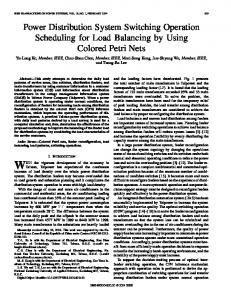
Fig. 1. Operation and schematic representation of (a) a single Pt/Nb2 O5 /Pt device, (b) a single Pt/NbO2 /Pt device, and (c) a merged serially connected device. Operation of the serial device shows the required switching region between −1.8 and +1.3 V (gray region), which inhibits switching.
Nb suboxide, NbOδ (δ < 2), filaments are formed with more oxygen vacancies (VO s) [7], [8]. However, NbO2 -based TS selection devices have received little attention compared with VO2 -based devices. In this letter, we demonstrate the feasibility of a Pt/NbO2 /Pt device for TS and a Pt/Nb2 O5 /Pt device for MS and obtain the required characteristics for crosspoint memory applications by connecting these two devices in series. Furthermore, the co-occurrence of TS and MS is observed in the asymmetric Nb2 O5 /NbO2 bilayer structure. II. E XPERIMENTS Metal Nb films, 30 nm thick, were deposited on Pt/Ti/SiO2 /Si substrates by the dc magnetron sputtering method. Then, polycrystalline Nb2 O5 and NbO2 thin films were formed by rapid thermal annealing at 500 ◦ C for 10 min with an oxygen pressure of 0.6 and 0.1 torr, respectively. In addition, 50-nm-thick Nb films were annealed at 500 ◦ C for 10 min at 0.1 torr and then for 5 min at 0.6 torr to form the bilayer Nb2 O5 /NbO2 structure. The crystallization of NbOx films was confirmed by X-ray diffraction. Subsequently, 50-nm-thick Pt top electrodes with a diameter of 50 µm were deposited on these films. Electrical measurements were carried out using an Agilent 4155C semiconductor parameter analyzer in air. III. R ESULTS AND D ISCUSSION Fig. 1(a) shows the bistable MS properties of Pt/Nb2 O5 /Pt device. After the initial electroforming process, the memory cell was switched to the low-resistance state (RLRS ).
0741-3106/$26.00 © 2011 IEEE
LIU et al.: CO-OCCURRENCE OF TS AND MS IN PT/NBOx /PT CELLS FOR CROSSPOINT MEMORY APPLICATIONS
By increasing the negative voltages imposed on the cell, a pronounced change in resistance from RLRS to the highresistance state (RHRS ) was observed at about −0.8 V (Vreset ); this is called the “RESET” process. Subsequently, an opposite “SET” process could also be seen when sweeping the positive voltage. The switching from the RHRS to RLRS occurs at about 1.9 V (Vset ), and nonvolatile switching was achieved. In general, broad dispersion of switching parameters in binary oxides is a big obstacle on the way of resistive memory application. In comparison with a previous work on Nb2 O5 operated in unipolar mode [7]–[10], better endurance and reproducibility properties are observed in bipolar mode due to the beneficial effect of the polarity reversal on limiting the oxygen runout process, which is in agreement with reports in other binary oxides [12]. Fig. 1(b) shows the monostable TS properties of Pt/NbO2 /Pt device. As the applied voltage increased from 0 to 2 V, the current suddenly increased at 1.8 V, called the threshold voltage (Vth,+ ). The electrical property of NbO2 changed from the insulating state (Rinsulating ) to the metallic state (Rmetal ). In contrast, as the applied voltage decreased from 2 to 0 V, the current suddenly decreased at 1.2 V, called the hold voltage (Vh,+ ). The electrical property of NbO2 went back to the insulating state. Similar IMT behavior is also observed in negative voltage sweeping. Generally, the I–V curve was symmetric with respect to polarity: Vth = |Vth,− | = |Vth,+ |, Vh = |Vh,− | = |Vh,+ |. In addition, no significant changes in Vth and Vh were observed even after 100 switching cycles, which is important for selection devices. For the crosspoint memory application, we connected two aforementioned electroformed devices by external contacts. Fig. 1(c) shows the combined I–V behavior with the gray region where the current is suppressed. The read voltage (Vread ) that we can choose is between Vth,4 and Vth,3 . By using, for example, a 1/2Vread scheme, the full voltage is applied only to the addressed cell [4]. The voltages at all nonaccessed cells are limited to values below the threshold voltage Vth,2 (Vth,3 , respectively) and are not affected. Note that the achievable safe margin for the 1/2Vread scheme depends on the Vreset and Vset in MS device and on Vth and Vh in TS device, and thus, it can be optimized by selecting the appropriate memory and switch materials. In addition, the window between Vth,3 and Vth,4 also depends on the RLRS in MS device and Rmetal in TS device. By using a resistor in series with the hybrid device with a resistance in the range of the LRS, the window will be more controllable and reducible. Based on the aforementioned results, we removed the middle Pt electrode and constructed asymmetric Nb2 O5 /NbO2 bilayer structures to reproduce the 1-memory + 1-switch properties of the aforementioned hybrid devices. Fig. 2(a) shows the asymmetric device structures and the measuring conditions. Ideal I–V behavior with built-in selectivity is shown in Fig. 2(b) in the gray region where the current is suppressed. The continuous “Read” processes (solid lines), after SET or RESET (line symbols), confirmed that these cells exhibit nonvolatile switching behavior with selective properties. It is noteworthy that all the threshold voltages (Vth,1 , Vth,2 , Vth,3 , and Vth,4 ) are significantly less than those of the serial cases in Fig. 1(c). To confirm the bilayer structure, the chemical composition of the NbOx films was examined by X-ray photoelectron spectroscopy (XPS) depth profiling. Fig. 2(c) shows the typical Nb
237
Fig. 2. (a) Schematic illustration of asymmetric Nb2 O5 /NbO2 bilayer memory devices and measurement conditions. (b) Typical I–V resistance switching measured under voltage sweeping. (c) XPS depth profiling spectra and deconvolution results of the Nb 3d core level of bilayer NbOx films. The black squares and yellow lines represent the measured and simulated spectra, respectively. The red, blue, black, and green lines represent the fitting curves for Nb2 O5 , NbO2 , NbOδ , and NbO phases, respectively. The relative area ratios are also shown.
Fig. 3. Schematic illustrations of (a) the structure of the initial bilayer Nb2 O5 /NbO2 devices and (b) the formation of metallic NbO2 filament and the movements of oxygen species during the electroforming transient. The center temperature of NbO2 layer rises as high as the IMT temperature of NbO2 due to Joule heating, which is denoted by the red color region. The simplified distributions of oxygen vacancies and free oxygen species (c) after electroforming, (d) during RESET process, (e) after RESET, and (f) during SET process.
spectra at different etch times from 0 to 18 min. A very distinct Nb 3d doublet was observed at the 2-min depth level, which indicates that a layer of Nb2 O5 was formed on the top layer of the NbOx films. Using a conventional fitting procedure, we simulated the XPS spectra of Nb 3d at the 8- and 13-min depth levels. Four doublets around 203.6, 204.5, 205.6, and 207.5 eV were required to simulate each XPS spectra and match the binding energies of NbO, NbOδ (1 < δ < 2), NbO2 , and Nb2 O5 , respectively [8]. Although localized phase separation occurs in our NbOx film, the typical I–V properties in Fig. 1(b) show TS behavior, which is consistent with the fitting results that the NbO2 phase is dominant. Therefore, it is suggested that the Nb2 O5 /NbO2 structure is formed, corresponding to the simplified schematic diagram in Fig. 3(a). During the electroforming process, the movement of oxygen species may be driven by both diffusion and drift as a result of the huge local temperature nonuniformity and the applied voltage, respectively [12]. With increasing the applied voltage,
238
IEEE ELECTRON DEVICE LETTERS, VOL. 33, NO. 2, FEBRUARY 2012
is going to be weakened. Nonetheless, this is only the first step toward a large passive crosspoint array. Clearly, more work is needed to improve the endurance and to scale the device down to the nanoscale. IV. C ONCLUSION
Fig. 4. (a) Typical I–V resistance switching measured under current sweeping and (b) dc endurance of Nb2 O5 /NbO2 bilayer structure devices.
the center temperature of NbO2 layer reaches the IMT temperature of NbO2 suboxide [Fig. 3(b)]. Then, the insulating NbO2 changes to metallic NbO2 , i.e., “switch on.” Here, the cathode shifts to the top of the NbO2 layer, i.e., a “virtual cathode.” The larger voltage drops at the Nb2 O5 layer. Neutral oxygen •• + atoms and VO s are generated near the anode [13], OxO → VO − 2e + O. Under a high electric field, these VO s drift toward the virtual cathode, and as a result, the filaments start to develop from the virtual cathode. In contrast, the evacuation of oxygen through Pt layers during electroforming may occur, as reported elsewhere [13], [14], because of the high mobility of the oxygen species in Pt layers. More oxygen atoms are removed from the oxide and chemisorbed at the Pt grain boundaries near the anode interface. Consequently, filaments consisting of metallic Nb suboxides NbOδ (δ < 2) are formed across the Nb2 O5 layer [7], [8]. Once the applied voltage is removed, the center temperature of NbO2 layer decreases, and then, metallic NbO2 filament goes back to insulating, i.e., “switch off.” The total resistance of the device remains high: RLRS + Rinsulating [Fig. 3(c)]. During the RESET process, the metallic NbO2 filament first formed, and then, the VO s recombine with the chemisorbed oxygen at the top of the Pt/Nb2 O5 interface [Fig. 3(d)]. After the RESET process, the total resistance remains high again: RHRS + Rinsulating [Fig. 3(e)]. During the SET process, the metallic NbO2 filament of NbO2 layer first forms, and then, the VO filaments across the Nb2 O5 layer form again [Fig. 3(f)]; this is similar to the electroforming process. As a result, the upper Nb2 O5 with local filaments shows MS, and the NbO2 layer shows TS. Furthermore, a current-controlled negative differential resistance (NDR) phenomenon with significant loop behavior was observed on the I–V curve under the current-sweeping mode, as shown in Fig. 4(a). This is a typical coexistence phenomenon of memristance and NDR, as observed below 155 K in the TiO2 /Ti4 O7 system [15]. In contrast, this co-occurrence of TS and MS in Nb2 O5 /NbO2 bilayer devices occurs at room temperature and is potentially attractive for a range of possible applications, including the above crosspoint memory arrays and oscillations [15]. Using the current-sweeping mode, more than 20 dc I–V cycles and a little fluctuation of resistive states have been recorded, as shown in Fig. 4(a) and (b), respectively. After 20 cycles, with the current increase at 1/2Vread , the selectivity
In this letter, we have demonstrated a method for applying bipolar RS materials to crosspoint memory arrays by connecting a Pt/Nb2 O5 /Pt memory and a Pt/NbO2 /Pt switch in series. Furthermore, by removing the middle Pt electrode, we observed the co-occurrence of MS and TS in the asymmetric Nb2 O5 /NbO2 bilayer structure. This MOM device can potentially reduce the fabrication complexity in high-density crosspoint memory arrays. R EFERENCES [1] G. Dearnaley, A. M. Stoneham, and D. V. Morgan, “Electrical phenomena in amorphous oxide films,” Rep. Prog. Phys., vol. 33, no. 3, pp. 1129– 1191, Sep. 1970. [2] F. A. Chudnovskii, L. L. Odynets, A. L. Pergament, and G. B. Stefanovich, “Electroforming and switching in oxides of transition metals: The role of metal–insulator transition in the switching mechanism,” J. Solid State Chem., vol. 122, no. 1, pp. 95–99, Feb. 1996. [3] M.-J. Lee, Y. Park, D.-S. Suh, E.-H. Lee, S. Seo, D.-C. Kim, R. Jung, B.-S. Kang, S.-E. Ahn, C. B. Lee, D. H. Seo, Y.-K. Cha, I.-K. Yoo, J.-S. Kim, and B. H. Park, “Two series oxide resistors applicable to high speed and high density nonvolatile memory,” Adv. Mater., vol. 19, no. 22, pp. 3919–3923, Nov. 2007. [4] M. Son, J. Lee, J. Park, J. Shin, G. Choi, S. Jung, W. Lee, S. Kim, S. Park, and H. Hwang, “Excellent selector characteristics of nanoscale VO2 for high-density bipolar ReRAM applications,” IEEE Electron Device Lett., vol. 32, no. 11, pp. 1579–1581, Nov. 2011. [5] D. V. Geppert, “A new negative-resistance device,” Proc. IEEE, vol. 51, no. 1, p. 223, Jan. 1963. [6] K. L. Chopra, “Current-controlled negative resistance in thin niobium oxide films,” Proc. IEEE, vol. 51, no. 6, pp. 941–942, Jun. 1963. [7] K. Jung, Y. Kim, W. Jung, H. Im, B. Park, J. Hong, J. Lee, J. Park, and J.-K. Lee, “Electrically induced conducting nanochannels in an amorphous resistive switching niobium oxide film,” Appl. Phys. Lett., vol. 97, no. 23, p. 233 509, Dec. 2010. [8] K. Jung, Y. Kim, Y. S. Park, W. Jung, J. Choi, B. Park, H. Kim, W. Kim, J. Hong, and H. Im, “Unipolar resistive switching in insulating niobium oxide film and probing electroforming induced metallic components,” J. Appl. Phys., vol. 109, no. 5, p. 054 511, Mar. 2011. [9] H. Sim, D. Choi, D. Lee, S. Seo, M.-J. Lee, I.-K. Yoo, and H. Hwang, “Resistance-switching characteristics of polycrystalline Nb2 O5 for nonvolatile memory application,” IEEE Electron Device Lett., vol. 26, no. 5, pp. 292–294, May 2005. [10] H. Sim, D. Choi, D. Lee, M. Hasan, C. B. Samantaray, and H. Hwang, “Reproducible resistance switching characteristics of pulsed laser–deposited polycrystalline Nb2 O5 ,” Microelectron. Eng., vol. 80, no. 1, pp. 260–263, Jun. 2005. [11] L. Chen, Q.-Q. Sun, J.-J. Gu, Y. Xu, S.-J. Ding, and D. W. Zhang, “Bipolar resistive switching characteristics of atomic layer deposited Nb2 O5 thin films for nonvolatile memory application,” Curr. Appl. Phys., vol. 11, no. 3, pp. 849–852, May 2011. [12] L. Goux, P. Czarnecki, Y. Y. Chen, L. Pantisano, X. P. Wang, R. Degraeve, B. Govoreanu, M. Jurczak, D. J. Wouters, and L. Altimime, “Evidences of oxygen-mediated resistive-switching mechanism in TiN\HfO2\Pt cells,” Appl. Phys. Lett., vol. 97, no. 24, p. 243 509, Dec. 2010. [13] D. S. Jeong, H. Schroeder, U. Breuer, and R. Waser, “Characteristic electroforming behavior in Pt/TiO2 /Pt resistive switching cells depending on atmosphere,” J. Appl. Phys., vol. 104, no. 12, p. 123 716, Dec. 2008. [14] J. J. Yang, F. Miao, M. D. Pickett, D. A. A. Ohlberg, D. R. Stewart, C. N. Lau, and R. S. Williams, “The mechanism of electroforming of metal oxide memristive switches,” Nanotechnology, vol. 20, no. 21, p. 215 201, May 2009. [15] M. D. Pickett, J. Borghetti, J. J. Yang, G. Medeiros-Ribeiro, and R. S. Williams, “Coexistence of memristance and negative differential resistance in a nanoscale metal–oxide–metal system,” Adv. Mater., vol. 23, no. 15, pp. 1730–1733, Apr. 2011.