Computer-Aided Fault to Defect Mapping (CAFDM) for Defect Diagnosis Zoran Stanojevic
Hari Balachandran
D. M. H. Walker
Fred Lakhani
Dept. of Electrical Engineering Texas A&M University College Station TX 77843-3124 Tel: (979) 862-6610 Fax: (979) 847-8578 Email:
[email protected]
Texas Instruments, Inc. Mixed Signal Products Dallas TX Tel: (214) 480-7602 Fax: (214) 480-7676 Email:
[email protected]
Dept. of Computer Science Texas A&M University College Station TX 77843-3112 Tel: (979) 862-4387 Fax: (979) 847-8578 Email:
[email protected]
International Sematech Yield Management Tools 2706 Montopolis Drive Austin TX 78741 Tel: (512) 356-7011 Fax: (512) 356-7640 Email:
[email protected]
Sri Jandhyala
Jayashree Saxena
Kenneth M. Butler
Texas Instruments, Inc. Mixed Signal Products Dallas TX Tel: (214) 480-7598 Fax: (214) 480-7676 Email:
[email protected]
Texas Instruments, Inc. P.O. Box 660199 MS 8645 Dallas TX Tel: (214) 480-1646 Fax: (214) 480-2356 Email:
[email protected]
Texas Instruments, Inc. P.O. Box 660199 MS 8645 Dallas TX Tel: (214) 480-1431 Fax: (214) 480-2356 Email:
[email protected]
Abstract Defect diagnosis in random logic is currently done using the stuck-at fault model, while most defects seen in manufacturing result in bridging faults. In this work we use physical design and test failure information combined with bridging and stuck-at fault models to localize defects in random logic. We term this approach computer-aided fault to defect mapping (CAFDM). We build on top of the existing mature stuck-at diagnosis infrastructure. The performance of the CAFDM software was tested by injecting bridging faults into samples of a streaming audio controller chip and comparing the predicted defect locations and layers with the actual values. The correct defect location and layer was predicted in all 9 samples for which scan-based diagnosis could be performed. The experiment was repeated on production samples that failed scan test, with promising results.
I. Introduction Fault localization or fault isolation is the process of identifying a region within an integrated circuit that contains a circuit fault, such as a short or open circuit. This region must be small enough that the defect causing the fault can be found and analyzed. This is very important for quickly debugging new products, ramping yields, identifying test and reliability problems in customer returns, and resolving quality assurance (QA) part failures. Advancing integrated circuit technology has resulted in more interconnect layers, smaller geometries, greater chip complexity, and flip-chip packaging. All of these greatly increase the complexity of fault isolation. Often a direct view of the defect from the front or backside of the chip is not available. This makes it increasingly difficult to locate the defect using defect localization methods that detect light or heat given off by the defect. Fault isolation has become the most time-consuming part of defect diagnosis, and often a diagnosis cannot be performed since the fault cannot be localized. As a result, fault isolation is listed as a difficult
challenge in the International Technology Roadmap for Semiconductors, with its complexity projected to grow by 142 times in the next 15 years [1]. The alternative to defect localization techniques is to use electrical tests to isolate the circuit fault, with the assumption that the defect is closely associated with the fault. In memory arrays this localization process is straightforward since there is a direct mapping between the bit fail map and the possible defect locations. In logic circuits such a straightforward mapping between electrical failures and locations is not available. Current state-of-the-art practice for localizing faults in logic circuits is to use a stuck-at fault diagnosis approach, which can be applied to circuits that are full scan or mostly scan. In this approach, a set of passing and failing vector outputs is captured, and fed into the diagnosis system. Diagnosis can be done with a variety of techniques such as Boolean difference [2] and critical path tracing [3], to identify a list of suspect nets where stuck-at faults best explain the observed failure patterns. The nets are ranked based on how many faulty output patterns they explain. The suspect list includes logically equivalent nets. For example, a stuck-at-0 fault on an AND gate output is equivalent to a stuck-at-0 fault on any of the AND gate inputs. Stuck-at diagnosis tools are commercially available, typically as part of an automatic test pattern generation (ATPG) system. Two examples are Mentor Graphics FastScanTM and IBM TestBenchTM. TestBench also supports the more general pattern fault model. The list of suspect nets from the diagnosis system can be visualized in the chip layout database using a tool such as Knights Technology LogicMapTM, which integrates the Knights CADNAVTM layout navigation system with FastScan [4][5]. The top few suspect nets are then examined with a scanning electron microscope (SEM) in order to locate the fault within the net. Voltage contrast is often used to locate open circuits within these nets. This
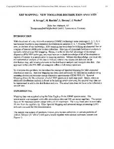
Electrical Test Data
Table 1. Project Metrics
Inline Data
Description
Suspect Nets
hours, days
SEM Isolation of Defects
hours
FIB, EDX etc. Physical Failure Analysis
Diagnosis
Run Diagnostic Test
minutes
Design & Test Data
Experience
Defect Knowledge Base
Likely Source
Figure 1. Current Defect Sourcing Approach current defect sourcing approach is shown in Figure 1. As shown, most of the time is spent in the SEM search. The drawback of using a stuck-at diagnosis approach is that most circuit faults are bridging faults, and the stuck-at fault model is not a very accurate model for them [6][7]. It is well known that the more accurately the fault model matches actual fault behavior, the better the diagnosis. The result of this limitation is that a significant fraction of the time, the real faulty nets do not appear on the list of suspects, or the faulty net is far down the ranked list of suspects, and so is never examined due to resource limitations. A second problem with the stuck-at approach is that it does not provide any ranking in terms of chip locations or process layers. Even if only one suspect net is reported, if it is a very large net, it may not be feasible to locate the fault with the SEM. This is particularly true if the net traverses primarily interior interconnect layers, and so is not directly visible from the top or backside of the chip. The increased number of interconnect layers in deep submicron circuits means that most signal routing is on an interior layer. Often such cases can only be diagnosed if, during fabrication, defect inspection detected a defect at the same location as one of the suspect nets. However inspection information is only available for a small fraction of chips, and is rarely available for customer returns. Overall, the result of these limitations is that the fault cannot be located in about 30% of all chips. This is not such
Goal
30%