This is achieved by adopting a set/reset behavior that is reminiscent of the operation of ... The goal of this paper is to propose a technique, derived from the properties of .... 3) Variations of delays due to the process variations. Here we ..... [5] D. Chinnery and K. Keutzer, âReducing the timing overhead,â in Closing the Gap ...
Coping with the variability of combinational logic delays J. Cortadella Univ. Polit`ecnica Catalunya Barcelona, Spain
A. Kondratyev Cadence Berkeley Labs Berkeley, CA
Abstract— This paper proposes a technique for creating a combinational logic network with an output that signals when all other outputs have stabilized. The method is based on dual-rail encoding, and guarantees low timing overhead and reasonable area and power overhead. This is achieved by adopting a set/reset behavior that is reminiscent of the operation of dynamic logic, but which is suitable for static logic as well. We also discuss various scenarios in which completion detection can be used to measure the delay of a synchronous circuit at fabrication time or at run time, and of an asynchronous circuit at run time. We conclude by showing, on a large set of benchmarks, the effectiveness of the proposed technique.
I. I NTRODUCTION Variability is a growing concern to digital circuit designers. While statistical timing analysis techniques try to apply various empirically derived models to combine together all sources of variability along a critical path, designers would like to have a way to measure rather than just predict the actual delay of a circuit. The reason is that a large fraction of circuits work faster or much faster than worst-case analysis would predict. Unfortunately delay fault testing is a costly proposition, because it requires the designer to start from a very expensive initial two-level representation, and then use only a subset of the logic optimization techniques [1]. Moreover, delay test patterns are more numerous than functional fault test patterns, and hence require more time on expensive testing machines. The goal of this paper is to propose a technique, derived from the properties of dynamic logic circuits but adapted to work with any static CMOS library, that enables ASIC designers to easily measure exactly when a combinational circuit is done computing. In practical terms, we guarantee that without almost any timing overhead and with some area overhead, every combinational logic block has an additional completion detection output that rises a few gate delays after the last primary output has settled. This paper improves with respect to the state of the art in the following directions, by proposing: • a technique for dual-rail network creation with much lower area, power and delay overhead than previously known techniques, and requiring only standard static CMOS gates. • a novel method, using timing assumptions rather than completion detection, for fast reset to the spacer (inactive) state. • an architecture for completion detection based on standard combinational gates, rather than Muller C elements, again exploiting timing assumptions in the reset phase. We show in Section VI that circuits obtained using our logic synthesis flow have a nominal delay which is on average within 33% of the corresponding circuit optimized using traditional techniques, with a 100% area overhead. However, by using the completion detection output their true delay can be measured and used to reliably latch their output values, thus reducing the margins that must be taken at design time. Moreover, most of this overhead is due to the completion detection network, that currently is generated to check all outputs, not just critical ones, and thus can be further optimized. Regarding power consumption, we can assume that it will increase approximately by a factor of 2, because our circuits do not have
L. Lavagno Politenico di Torino Torino, Italy
C. Sotiriou ICS-FORTH Crete, Greece
any glitches (which are known to consume about half of the active power in combinational logic), but have on average twice as much capacitance and twice as many transitions as traditional combinational logic. The increase in transitions due to the set/reset phase operation described below, approximately offsets the reduction due to absence of glitches. Leakage and dynamic power thus approximately doubles, due to the doubling of active area and wiring. Two key assumptions motivate the use of circuits with completion detection: •
•
The difference between worst case and true delays is in the range of 60-100% (see the detailed breakdown of worst case delay penalties in Section II), and will most likely increase over time. The fraction of “truly critical” register-to-register combinational logic blocks is relatively small (10-20% according to internal sources). Many such blocks, especially in ASIC designs, have significant timing slack.
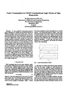
Based on these two assumptions, we believe that, by using circuits with completion detection, one can achieve at least 25% of performance increase with 10% to 20% penalty in power and area purely remaining in the synchronous domain. In this paper we are considering the following application scenarios for our design flow: 1) Fully synchronous design, when the circuit must be tested off-line for operation speed and binned accordingly. In this scenario, a few test patterns are applied (preferably in normal operation mode, but also possibly in scan mode) in order to sensitize the longest paths, and the completion detection output is sensed in order to determine the speed. 2) Almost synchronous design, when the circuit must be robust with respect to dynamic parametric variation, due e.g. to temperature and/or supply voltage. In this case, failures to raise the completion output in time can be used to slow down or stop the clock, or to trigger a system reset in the worst case. 3) Asynchronous circuit design, in which one takes advantage of both parametric variations and data-dependent computation times (e.g. it is well-known that the average case delay for a ripple carry adder is logarithmic in the number of bits, assuming uniformly distributed input values). 4) Low-EMI design, in which the circuit must absorb current from its power supply with patterns that do not depend on the actual data values, in order to minimize emission and make security attacks based on Differential Power Analysis much harder. II. M OTIVATION The main advantage of completion detection in combinational circuits is the ability to run the circuit using true rather than worst-case delays. Figure 1 shows the delay penalty stemming from two main factors: a) static timing analysis technology (the industry standard for doing timing sign-off) that estimates delays for the worst case scenario and b) clocking overhead in the conventional synchronous methodology.
Combinational overhead Real Computation time 100%
Fig. 1.
Library: worst vs typical 50%
Crosstalk, IR-drop 20%
Clock overhead Process Clock variability skew 30% 10%
Unbalanced stages 20%
Delay penalties in the modern synchronous methodology
These penalties are: 1) The difference in the library files between typical and worst case. This may account for up to a 50% penalty. 2) Conservative estimation of the slowdown caused by signal integrity violations: namely IR drop and crosstalk. Each of them could be responsible for a 10% penalty [2], [3]. 3) Variations of delays due to the process variations. Here we assumed it to be about 30% for the latest technologies (see e.g. [4]), though more aggressive forecasts also exist. 4) Clock skew, which is about 10% of the clock cycle for the modern ASIC methodology [5]. 5) Non-ideal balancing of synchronous stages, which increases the clock cycle with respect to the mean cycle time by up to 20% [5]. The first three sources come from the combinational logic itself, while the last two are coming from the clocking scheme. Summing these penalties gives a quantitative estimation of the margin that separates true from worst-case delays. This margin shows the optimization room that is available when implementing circuits with completion detection. Part of this advantage is offset by the overheads due to the dual rail conversion, the two-phase operation and the completion detection logic itself. However, as shown in Section VI, these penalties are lower than the combinational logic penalty cited above. Clock penalties, as well as exploiting data-dependent delays, may provide additional performance improvements when the circuits with completion detection are used in an asynchronous environment, as discussed below. III. P REVIOUS W ORK Our work has been inspired by two active research areas: asynchronous design and synthesis of dynamic logic. Asynchronous systems do not rely on timing assumptions to reason about settling of data at the circuit outputs. Instead they coordinate behaviors in a causal way. As a result, logic synthesis for asynchronous circuits needs to take care not only of the functionality but also the proper ordering of the gates switching. This is achieved by introducing redundancy a) in the protocol with which the circuit input/output is handled (also called “mode of operation”) and b) in the circuit itself, in order to derive information about completion of the evaluation. One of the most popular operation modes in asynchronous design alternates data communication between set and reset phases [6], with the two-fold goal of: a) providing a clean separation between two consecutive data sets and b) ensuring monotonic behavior at circuit outputs, avoiding spurious transitions known as hazards [7]. Circuit inputs and outputs change from a spacer in the reset phase, which carries no data information and serves only synchronization purposes, to a proper data codeword during the set phase, and then back to the spacer in the next reset phase. The simplest scheme for such communication is given by dualrail encoding, in which each signal a is represented by two wires a.t and a.f : a = 1 is encoded as a.t = 0, a.f = 1, and a = 0 is encoded as a.t = 1, a.f = 0. The spacer for the reset phase is usually encoded as a.t = a.f = 0 (the complementary encoding,
with spacer a.t = a.f = 1 and exactly one signal falling to indicate a valid codeword, can also be used). An attractive property of dualrail encoding is the capability to determine that a proper codeword has settled by checking the codeword itself, without making timing assumptions. Indeed, if the circuit is hazard-free, then the fact that exactly one of the wires in each dual-rail pair goes high, tells that the output has settled and the set phase is over. Two regular methods for implementing an arbitrary Boolean network with two-phase operation and dual-rail encoding were suggested in [8] and [9]. In both techniques every node of a network representing Boolean function f is implemented by two logic cones f.t and f.f , where f.t represents the original function f , while f.f represents its inverse f . In the DIMS method [8] f.t and f.f are implemented as sums of minterms, with every minterm being realized by a Celement (a sequential gate with equation c = ab + ac + bc). When inputs make transitions from the spacer to a codeword, then one (and only one) output rises. Moreover, since only one of the minterms in the cone can rise during the set phase, the rising of the corresponding output rail happens as the last transition in the cone. In this way the information about completion is transmitted from inputs of the cone to its outputs, providing 100% observability for every circuit path. This advantage, however, comes at a significant cost, because none of the conventional logic optimizations are possible in DIMS circuits without losing completion detection properties. This difficulty is partially addressed in the NCLX design flow [9] which is the closest approach to ours. In [9] a dual-rail network is created by 1) simply adding duals to every gate and 2) eliminating inversions by using corresponding complementary rails. Completion detection is carried out separately from the data evaluation. Partitioning a circuit into loosely connected functional and completion detection parts allows a designer using the flow described in [9] to optimize and implement circuits using the full power of logic synthesis and EDA tools. This results in lowering the area penalty, which however cannot be reduced beyond 2x because of the dual-rail encoding. Such area overhead may or may not be acceptable depending on other advantages (speed/power) that these circuits could provide. The main goal of detecting completion is to cover the increasing gap between “true” and worst case nominal delays. Unfortunately this is impossible in both approaches mentioned above, because the speed advantage, due to using the true delays instead of worst-case approximations, is offset by the need to use two operational phases (set and reset) in a single computational cycle. The nearly 2x delay penalty from the two-phase operational mode is difficult to recover through reducing delays from worst case to true. Dual-rail networks with two-phase operation are also used in dynamic logic synthesis [10], [11]. In the following we discuss about domino logic, even though most considerations extend to other dynamic logic styles. A major limitation of domino logic is that it can only implement non-inverting logic (other styles require strict layering of, e.g. pre-charged and pre-discharged gates). Hence complements of internal signals need to be realized through separate cones of logic using dual functions and giving rise to partially or fully dual-rail circuits. Similar to asynchronous systems, dynamic circuits work in two phases, namely pre-charge and evaluate. This feature, however, allows dynamic logic to achieve significant speed improvements over static CMOS, because the reset (pre-charge) phase is very short. Unfortunately, the inherent noise sensitivity and chargesharing problems associated with this design style limit its application to small timing-critical portions of systems, which are usually handdesigned.
Area
P
4x
P
N
P
3x Our work
P
P
P
NCLX
N
P
2x
(a)
Dynamic logic 0.5x
Fig. 3.
Static CMOS
1x
1x
Delay
P
N
DIMS
P
P P
? N (b)
(a) Monotonic network, (b) non-monotonic network.
xi is positive and fi is increasing in xi , or xi is negative and fi is decreasing in xi . A node ni with local function fi is negative if for each input xi in its local fanin it holds that • xi is negative and fi is increasing in xi , or • xi is positive and fi is decreasing in xi . A node is monotonic if it is either positive or negative. While this definition works for any network which admits a consistent labeling of each node (including primary inputs and primary outputs) as positive or negative, for the sake of simplicity in the following we assume that all primary inputs are dual-rail encoded with spacer 00, and hence are defined to be positive. Definition 4.4 (Monotonic and positive Boolean networks): A Boolean network is monotonic (MBN) if all its nodes are monotonic. An MBN is positive (PBN) if all its nodes are positive (e.g. a domino logic network is positive). Theorem 4.1 (Hazard-free behavior of an MBN): An MBN is hazard-free under a monotonic input transition. Proof: See [12] Figure 3 depicts a monotonic and a non-monotonic network. The labels P and N indicate the positive and negative nodes, respectively. The network in Fig. 3(b) is not monotonic since it is not possible to assign a phase to the output node. Note that the input transition 000 → 111 applied to all inputs may produce a glitch at the output, if the inverter and the OR gate switch before the AND gate. •
•
Fig. 2.
Architecture-dependent area-delay trade-offs
Our paper makes an attempt to take the best of both worlds and develop a design flow that combines performance advantages inherent in true delay measurement, with the robustness and simplicity of static standard cell CMOS, all within a standard ASIC design flow. The objective of this this work in terms of area-delay trade-offs is shown in Figure 2. The figure already takes into account the fact that circuits with completion detection (our work, DIMS and NCLX) work with true delays, and hence faster than static CMOS. IV. M ONOTONIC B OOLEAN NETWORKS A. Hazards Glitches in combinational circuits are called hazards [7]. A hazard is a transient change on a signal caused by the gate propagation delays. To characterize the dynamic behavior of a combinational circuit we need to define the allowed transitions at the primary inputs of the circuit. We will focus on a specific set of transitions that are relevant for the work in this paper. Definition 4.1 (Monotonic Input Transition (MIT)): A monotonic input transition consists of the change in the value of a subset of primary inputs in the same direction, i.e. all changes are either 0 → 1 or 1 → 0. Definition 4.2 (Monotonic operation mode (MOM)): The monotonic operation mode works by iteratively alternating two sub-phases, each of which is a Monotone Input Transition (MIT): (a) a subset of the inputs changes monotonically and (b) a subset of the outputs changes monotonically. In order to use this mode of operation for completion detection, the set of changing outputs must be known in advance. In particular, with dual-rail encoded signals exactly one input and one output in every pair changes value in each phase. Dual-rail operation normally alternates (a) and (b) sub-phases in which half of the inputs and half of the outputs rise in the set phase, with (a) and (b) sub-phases in which all inputs and outputs return to zero in the reset phase. B. Monotonic Boolean networks We assume the reader to be familiar with the basic concepts on Boolean functions and Boolean networks. Each non-input node ni of a Boolean network has an associated Boolean function fi in terms of its local fanin. Now we introduce the concept of monotonicity of the nodes of a Boolean network. Monotonicity is related to the fact that each node can be assigned a positive or negative phase in the network, which reflects the direction in which its output changes due to a change in value of primary inputs. Definition 4.3 (Monotonicity): A node ni with local function fi is positive if for each input xi in its local fanin it holds that
C. Use cases Combinational logic with completion detection can be used in two different environments: synchronous and asynchronous (see Figure 4(a) and (b)). In the synchronous environment, the output of the completion detector (denoted by CD in Figure 4(a)) is used to check whether a circuit can work at a given clock frequency. If a change at the output of a completion detector happens before the clock edge, then data inputs of receiving flip-flops have settled before the clock rises and no synchronization fault occurs. If, however, the completion detector makes a transition after the clock edge, then there are chances that erroneous values have been stored in flip-flops, and the error signal must be raised. The error signal may be used: • during production test to bin chips according to their performance • to provide an on-line testing capability, assuming that the system may roll back and repeat the computation cycle or is capable of stretching the clock. In order to give a qualitative estimation of the potential performance benefits from using circuits with completion detection, let us compare their cycle time with the cycle time of conventional synchronous designs. The cycle time in a synchronous circuit must satisfy the following timing constraints:
a.t b.f CL
FF
CL
FF CD
reset
FF a b
CD
reset
comp
comp
r s
c d
a.f (a)
Fig. 5. M
M
CLK gen
M
S
CD
reset Cm
CLK gen
(b)
x.t y.f y.t x.f
(c)
From single-rail (a) to dual-rail (b), and technology mapping (c).
S
CD
V. T RANSFORMATIONS TO OBTAIN AND PRESERVE A M ONOTONIC B OOLEAN N ETWORK
Cs
CLK gen
CLK gen
CLK gen
CLK gen
(b)
Fig. 4.
a.t x.t b.f c.f b.t y.f d.t d.f y.t c.t x.f a.f
CL
S reset
s.f r.f
CLK (a) CL
x d.f
s.t
y c.t
Error
Error
b.t c.f d.t
r.t
Architectures with completion detection
CLmax + Tskew + Tsetup + TCQ max ≤ Tcycle setup constraint hold constraint CLmin + TCQ min ≤ Thold + Tskew In these inequalities CLmax and CLmin stand for worst and best case propagation delays through combinational logic, while TCQ is the clock-to-output delay of a flip-flop. The cycle time in a circuit with a completion detection also needs to satisfy hold and setup constraints which are: CLtrue + Tskew + Tsetup + TCQ max + Treset max + TCD ≤ Tcycle CLmin + TCQ min ≤ Thold + Tskew where CLtrue is the true delay of combinational logic, while TCD and Treset max are the delay overheads of the architecture with completion detection (delays of the completion detector and reset phase respectively). A circuit with completion detection must satisfy an additional timing assumption in order to function correctly in the reset phase: Treset min ≤ Thold where Treset min is the minimum delay for propagating spacer values to the outputs of the combinational logic. This constraint is similar to the hold constraint and is needed to ensure that spacer does not overwrite data values before they are stored in registers. The reset signal can be derived directly from the clock, assuming that it has an (asymmetric) duty cycle of Treset max /Tcycle . In this case the reset phase is triggered by the rising edge of the clock and its duration is defined by the width of a clock pulse. One can see that a synchronous architecture with completion detection provides a performance advantage if CLtrue + Treset max + TCD < CLmax Experimental results give a quantitative estimation of Treset max and TCD , showing that the conditions of the above inequality are indeed met very often. In order to use circuits with completion detection in an asynchronous environment, one can exploit standard micropipeline-based architectures [13]. For example, they are suitable for desynchronized circuits [14], which are derived from synchronous synthesizable specifications. The only difference is that the request signals triggering controllers are derived from completion detectors rather than from matched delays, as shown in Figure 4(b).
A. Conversion to Monotonic Boolean Network We can generate an MBN from a generic Boolean network by using a special encoding of inputs and outputs: the dual-rail code. We now present a technology-independent conversion to a MBN1 : 1) From each primary input x, two primary inputs xt and xf are created to represent the true and false evaluations of x. 2) From each node implementing the function yi = fi (x1 , . . . , xn ), two nodes are created with the functions ` ´ yit = DR (fi (x1 , . . . , xn )) yif = DR fi (x1 , . . . , xn ) where DR denotes the transformation of the function into positive unate, changing also its input signals from xi to xti and xfi as appropriate. Formally, the transformation DR can be recursively defined as follows, using Shannon’s expansion: DR(0) = 0 DR(1) = 1 DR(x · fx + x · fx ) = xt · DR(fx ) + xf · DR(fx ) As an example, the function y = ab + b(c + d) would be converted into ` ´ y t = DR “ab + b(c + d) ”= at bf + bt (ct + df ) y f = DR ab + b(c + d) = (af + bt )(bf + cf dt ) Figure 5 depicts a complete example of how a single-rail circuit (a) is converted into a dual-rail circuit (b). After technology mapping, the circuit in Fig. 5(c) can be obtained. In [15], a set of transformations that do not introduce new hazards in Boolean networks was presented. They extend the set originally given in [7] and include De Morgan’s laws, dual global flow, global flow, tree decomposition, gate replication, collapsing, kernel-factoring and cube-factoring. These transformations cover, among others, the conventional algebraic optimizations performed during technologyindependent logic synthesis [16] and during technology mapping. Thus, logic synthesis and technology mapping can be performed on MBNs as long as the set of transformations fall into the category of hazard-non-increasing. B. Fast reset and completion detection An MBN would operate at half the speed of its original counterpart, due to the need for resetting all primary inputs before another monotonic phase can begin. We can speed up this reset phase by inserting signals that force gate outputs to their “quiescent” value (i.e. to the value that they assume when all dual-rail inputs are at 0, in the spacer condition). Of course there is a trade-off here between the number of gates which are reset in this manner (the 1A
conversion for technology-mapped circuits is also presented in [12]
more numerous, the faster becomes the reset phase) and the large capacitance connected to the reset signal (which may end up slowing down the circuit too much). We are in the process of evaluating what is the optimal fraction of the total number of levels where one should insert the reset signal, and what optimization algorithms can be used here. Gates with fewer inputs are obviously better candidates, since the delay of a gate increases quadratically with the number of transistors in series. Furthermore, the network that detects when all outputs have stabilized can be built simply by using an or gate for each dualrail pair, whose output rises when one of the signals rises, and a tree of and gates. VI. R ESULTS The method described in Sect. V has been automated and a design flow has been created. The flow is compatible with commercial EDA tools and, in particular, has been integrated with the Synopsys Design CompilerT M . The steps of the flow are the following: (1) conversion from single-rail to dual-rail, (2) technology mapping and (3) buffer optimization. The flow was applied to the largest IWLS combinational benchmarks and to a set of larger Verilog RTL circuits, i.e. the pipeline stages of a DLX CPU. All circuits were mapped to the UMC 0.18µm technology library. The results for the DLX CPU were obtained from the physical layour (after placement and routing). The results are shown in Table VI. The shorthands SR, DR, DR R and DR CD in the column labels correspond to Single-Rail, DualRail, Dual-Rail with Fast Reset, and Dual-Rail with Fast Reset and Completion Detection respectively. Percentage increase is computed as 100 × (DR − SR)/SR for both area and delay. The delay penalty for the data phase of the dual-rail circuits, indicated by columns DR and DR R, is relatively small. The penalty due to completion detection, which is currently larger, can be reduced by considering it only for critical outputs. The area penalty is about two-fold. As dual-rail circuits operate using the two-phase discipline, the reset phase delay must also be taken into account. For the circuits presented here, with reset employed every 6 circuit levels, the reset time is between 0.16ns and 0.22ns. VII. C ONCLUSIONS This paper proposes a novel technique to create circuits with completion detection, based on a dual-rail encoding. We describe both theory ensuring correct hazard-free operation, and implementations working both at the technology-independent and at the technologydependent levels. The experimental results show that a 100% area and power increase and a 30% delay increase are sufficient to obtain a circuit that is fully able to signal when its outputs have stabilized. Bearing in mind the margin of 60-100% between worst case and true delays, one can conclude that circuits with completion detection could operate at 25-65% higher clock frequencies than traditional ones. This enables for the first time a trade-off between applying completion detection to the whole design, and achieving the 2565% speedup with 100% area and power penalty, versus applying it only to the most critical stages of logic, and gaining less speed with significantly smaller penalty in area and power. Exploring this trade-off is left to future work. Acknowledgments. This work has been partially funded by CICYT TIC2001-2476 and ACiD-WG (IST-1999-29119).
R EFERENCES [1] S. Devadas and K. Keutzer, “Synthesis of robust delay-fault testable circuits: Theory,” IEEE Transactions on Computer-Aided Design, vol. 11, no. 1, pp. 87–101, Jan. 1992. [2] “User guide,” in Celtic User Manual, Cadence Design Systems, Inc., 2004. [3] “Datasheet,” in Physical Studio Datasheet, Sequence Design, Inc., 2003. [4] S. Nassif, “Modeling and analysis of manufacturing variations,” in Proc. of Asia and South Pacific Design Automation Conference, May 2001. [5] D. Chinnery and K. Keutzer, “Reducing the timing overhead,” in Closing the Gap between ASIC and Custom: Tools and Techniques for HighPerformance ASIC design. Kluwer Academic Publishers, 2002, ch. 3. [6] C. L. Seitz, “System timing,” in Introduction to VLSI Systems, C. A. Mead and L. A. Conway, Eds. Addison-Wesley, 1980, ch. 7. [7] S. H. Unger, Asynchronous Sequential Switching Circuits. New York: Wiley-Interscience, John Wiley & Sons, Inc., 1969. [8] J. Sparsø and J. Staunstrup, “Delay-insensitive multi-ring structures,” Integration, the VLSI journal, vol. 15, no. 3, pp. 313–340, Oct. 1993. [9] A. Kondratyev and K. Lwin, “Design of asynchronous circuits by synchronous CAD tools,” in Proc. ACM/IEEE Design Automation Conference, June 2002. [10] M. Prasad, D. Kirkpatrick, R.Brayton, and A. sangiovanni Vincentelli, “Domino logic synthesis and technology mapping,” in Proc. International Workshop on Logic Synthesis, vol. 1, 1997. [11] R. Puri, A. Bjorksten, and T. Rosser, “Logic optimization by output phase assignment in dynamic logic synthesis,” in Proc. International Conf. Computer-Aided Design (ICCAD), 1996, pp. 2–8. [12] J. Cortadella, A. Kondratyev, L. Lavagno, and C. Sotiriou, “Coping with the variability of combinational logic delays,” www.lsi.upc.es/˜jordicf/publications/pdf/ iccd04rep.pdf, July 2004. [13] I. E. Sutherland, “Micropipelines,” Communications of the ACM, vol. 32, no. 6, pp. 720–738, June 1989. [14] I. Blunno, J. Cortadella, A. Kondratyev, L. Lavagno, K. Lwin, and C. Sotiriou, “Handshake protocols for de-synchronization,” in Proc. International Symposium on Advanced Research in Asynchronous Circuits and Systems. IEEE Computer Society Press, Apr. 2004, pp. 149–158. [15] D. S. Kung, “Hazard-non-increasing gate-level optimization algorithms,” in Proc. International Conf. Computer-Aided Design (ICCAD), 1992, pp. 631–634. [16] R. Brayton, G. Hachtel, and A. Sangiovanni-Vincentelli, “Multilevel logic synthesis,” Proceedings of the IEEE, vol. 78, no. 2, pp. 264–300, 1990.
IWLS Benchmarks C1908 C2670 C3540 C5315 C7552 alu4 apex6 dalu des frg2 i10 i2 i7 i8 i9 k2 pair rot vda x3 x4 DLX Circuits DLX IF DLX ID DLX EX DLX MEM average
SR delay (ns)
SR area (µm2 )
DR delay increase
DR area increase
DR R delay increase
DR R area increase
DR CD delay increase
DR CD area increase
2.07 1.53 2.59 2.08 2.16 1.85 0.89 1.34 1.46 0.94 2.34 0.73 0.71 1.05 1.09 1.18 1.49 1.27 0.96 0.72 0.61
9709 13592 16665 33737 35294 9079 11006 10998 51910 10965 32489 3062 8754 13149 9612 14942 21544 9132 9059 10669 5749
-4% 3% 7% 6% 26% 0% 11% -2% 34% 3% 5% 9% -40% -11% -5% 0% 6% 9% 0% -2% -3%
79% 79% 79% 77% 81% 80% 91% 84% 73% 67% 80% 94% 62% 86% 77% 87% 86% 79% 90% 91% 72%
-0% 9% 14% 40% 32% 4% 15% 2% 35% 5% 41% 16% -39% -7% -0% 4% 12% 13% 6% 4% 3%
91% 93% 90% 90% 100% 90% 107% 94% 99% 82% 96% 102% 72% 95% 85% 102% 98% 95% 99% 203% 86%
12% 34% 23% 58% 50% 13% 57% 18% 63% 45% 59% 21% 8% 25% 29% 30% 37% 42% 35% 55% 59%
99% 121% 94% 103% 111% 93% 139% 99% 108% 116% 113% 105% 96% 115% 109% 112% 116% 138% 108% 236% 116%
0.82 4.01 3.46 0.50 1.52
18340 158709 121404 3294 25791
-4% 7% -2% -18% 3%
55% 68% 88% 64% 77%
-1% 11% 5% -16% 11%
69% 86% 103% 94% 95%
47% 24% 16% 58% 33%
89% 103% 105% 184% 109%
TABLE I E XPERIMENTAL RESULTS .