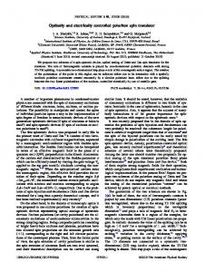
Device structure and simulation parameters: Fig. 1 shows the crosssectional view of the proposed configurable polarity-based device structure, along with the external bias required to dynamically configure as an n-, p-TFET or an n-, p-MOSFET. We chose an ultrathin lightly
I
50 nm
I
50 nm
I
Ls
PG- 1
CG Tox = 0.8 nm
I
Ls
NiSi
P-silicon, TSI = 10 nm
D
Tox = 0.8 nm CG
PG- 1
type
MOSFET N-type P-type
I
50 nm
I
PG- 2 NiSi
PG- 2
S
TFET N-type P-type
PG-1
+ 1.2 V
– 1.2 V
+ 1.2 V
– 1.2 V
PG-2
+ 1.2 V
– 1.2 V
– 1.2 V
+ 1.2 V
Fig. 1 Cross-sectional view of configurable proposed device and external bias required for PGs
1.0 0.5 0
–0.5
–1.0
CB PG-1
CG
PG-2
VB n-MOSFET p-MOSFET
energy level, eV
Introduction: Tunnel field-effect transistors (TFETs) have major performance advantages over conventional MOSFETs due to the steepness of the transition slope from the off to the on state and very low off-state current. For moderate performance requirements, TFETs not only offer a better Ion/Ioff ratio, but also power savings and superior performance for the same voltage over MOSFETs [1]. However, for higher performance requirements, MOSFETs are attractive options [2, 3]. To achieve computationally efficient (simultaneous improvement in performance and power savings) FETs, both (TFETs and MOSFETs) transistors need to be integrated into circuits that can extend the Boolean functionality of the complementary metal–oxide–semiconductor (CMOS) technology. Further, lightly doped TFETs and MOSFETs offer less susceptibility to random variability in device performance due to reduced random dopant fluctuations (RDFs) and an absence of an abrupt doping profile at the S/D junctions; as a result, the proposed device may have significantly less sensitivity to process parameter variations, reduced fabrication complexity, the thermal budget and leakage current [4]. In this Letter, we propose an electrically doped dynamically configurable double-gate FET that can be configured dynamically by applying an appropriate polarity bias. In other words, the same device can be operated either as a TFET or MOSFET, hence yielding the benefits of both devices and the freedom to dynamically switch between high-performance and low-power (power saving) applications. Apart from dynamically switching between the TFET and the MOSFET, the polarity (n- and p-type) of the proposed device can also be controlled dynamically. The concept of dynamic configurability is based on the electrically doped source and drain regions, instead of relying on the abrupt doping profile at the junctions. The proposed device employs the same concept for realisation of dynamically configurable TFETs and MOSFETs, and they can be programmed dynamically to an n-TFET (or MOSFET) or p-TFET (or MOSFET). Recently, configurable logic gates using polarity-controlled silicon nanowire (SiNW) FETs have been demonstrated with configurable n- and p-MOSFETs using extra polarity gates (PGs) and they have shown good potential for higher packaging density and compatibility with the CMOS process [5, 6]. For the proposed device, we chose lightly doped double-gate FETs as they exhibit good scalability and better short-channel effects [7]. In our device, two sets of gate electrodes are employed: (a) the control gate (CG) acts identically to a conventional gate for switching on and off the device and (b) PGs embedded on the side regions of the channel close to the source and drain contacts; they control the polarity and conduction mechanism, i.e. the nature of the device, hence, dynamically switch to an n-TFET (or MOSFET) and a p-TFET (or MOSFET). Further, we show that the proposed configurable TFET exhibits symmetric IDS − VGS characteristics, which are indispensable for configurable logic gates. However, the proposed device also has the drawback of requiring extra PGs; hence, extra metal deposition and isolation are required which may cause more parasitic effects. Two-dimensional (2D) SILVACO TCAD simulation results show that the proposed device (either n-, p-TFETs or n-, p-MOSFETs) has good agreement over conventional static devices and has the requisite qualities for low-power and high-performance applications.
1.0 CB n - MOSFET 0.5 p- MOSFET VB 0 CB –0.5 PG-1 PG-2 –1.0 VB
0 0.04 0.08 0.12 0.16 distance along x-axis, µm a
0 0.04 0.08 0.12 0.16 distance along x-axis, µm b
n - TFET 2.0 CB p- TFET 1.5 CB 1.0 VB 0.5 VB 0 –0.5 –1.0 –1.5 PG-1 CG PG-2 –2.0 0 0.04 0.08 0.12 0.16 distance along x-axis, µm c
2.0 CB CB 1.5 1.0 VB VB 0.5 n - TFET 0 p- TFET –0.5 –1.0 –1.5 PG-1 CG PG-2 –2.0 0 0.04 0.08 0.12 0.16 distance along x-axis, µm d
energy level, eV
The concept of an electrically doped dynamically configurable fieldeffect transistor (FET) is presented, which provides freedom to dynamically switch between a high-performance MOSFET and a low-power tunnel FET that can be ideal for complementary circuit implementation. The charge carrier concentration, polarity and conduction mechanism of the device are precisely controlled by the appropriate application of an external polarity control signal, instead of the conventional ion-implantation process. Two-dimensional TCAD simulation results confirm the dynamic configuration of the proposed device and good functionality agreement with existing devices as well as it having the requisite qualities for low-power and high-performance applications.
energy level, eV
A. Lahgere✉, C. Sahu and J. Singh
doped (1 × 1015 cm−3) p-type SiNW of thickness (TSI) 10 nm having a uniform carrier concentration from the source to the drain region. The simulation parameters considered in this Letter are gate length (control and polarity), is 50 nm; effective gate oxide thickness (TOX), 0.8 nm; and spacer length (LS) at the source and drain side, 5 nm, in line with recent work relating to junctionless TFETs [8] and polarity-controlled SiNWFETs [5]. The source and drain regions (either p+ or n+) are electrically induced on an ultrathin lightly doped silicon body by applying an external bias to the PGs of the same metal, such as TiN, as the control gate. Further, the source and drain contacts are made up of nickel silicide (NiSi) as it features a near midgap work function with a barrier height of 0.45 eV. The configurable device structure shown in Fig. 1 was simulated using the 2D ATALS TCAD tool [9]. The working mechanism of the proposed device is illustrated by electrical characteristics and functionalities supported by the TCAD simulator after incorporating different models. For the MOSFET, the hydrodynamic transport model is enabled [5], whereas for the TFET the non-local band-to-band tunnelling model is enabled in order to account for the tunnelling mechanism [7].
energy level, eV
Electrically doped dynamically configurable field-effect transistor for low-power and high-performance applications
Fig. 2 Band diagrams of configurable n- and p-MOSFETs under off-state (Fig. 2a) and on-state (Fig. 2b) condition, and n- and p-TFETs under offstate (Fig. 2c) and on-state (Fig. 2d) condition
Simulation results and discussion: To show the functionality of a configurable FET, initially we simulated energy band diagrams for the different configurations. Fig. 2a shows n-type (VCG = 0 V, VPG-1 = VPG-2 = 1.2 V and VDS = 50 mV) and p-type (VCG = 0 V, VPG-1 = VPG-2 = −1.2 V and VDS = −50 mV) MOSFETs in the off-state along the horizontal cut-line near the top surface of the silicon film of the proposed device. Similarly, on the application of the control signal (i.e. on-state), there is an occurrence of appropriate band bending for n- and p-type MOSFETs, as shown in Fig. 2b. Similarly, Fig. 2c shows an energy band diagram for n-type (VCG = 0 V, VPG−1 = 1.2 V, VPG−2 = −1.2 V and VDS = 50 mV) and p-type (VCG = 0 V, VPG−1 = −1.2 V, VPG−2 = 1.2 V and VDS = −50 mV) TFETs in the off-state. One can observe that both devices (MOSFETs and TFETs) in off-state offer a sufficient barrier and obstruct the flow of carriers. Similarly, on the application
ELECTRONICS LETTERS 6th August 2015 Vol. 51 No. 16 pp. 1284–1286
CG
PG-2
ON - state : electron
n+
p
n+
n+
PG-1
CG
PG-2
PG-1
CG
PG-2
PG-1
CG
PG-2
PG-1
CG
PG-2
source drain OFF - state : electron
n+
i
PG-1
CG
p+
PG-2
10–5
source
n+
n+
source drain ON - state : electron
n+
n+ PG-1
CG
e–
increasing
h+
increasing a
IDS, A/µm
nMOSFET n - TFET
PG-1 drain
MOSFET TFET
10–7 10–9 10–11
p+
10–13
PG-2
10–15
p -type n-type
–1.2 –0.8 –0.4 0
0.4 0.8 1.2
VCG, V b
Fig. 3 Contour plots of electron and hole carrier concentrations in off-state and on-state conditions for configurable FET (Fig. 3a), and transfer characteristic of n-, p-TFETs and n-, p-MOSFETs (Fig. 3b)
Impact of spacer length (LS) and offset between PG-1 (or PG-2) and NiSi contact: Spacer length (LS) in the proposed FET plays a significant role in maintaining the configurability, and tunnelling rate in a TFET; therefore, we have considered the same LS on both sides of the drain and source, and observed the impact of its scaling. A larger LS may relax the fabrication process constraints while degrading the tunnelling rate, and result in poor Ion and SS. Figs. 4a and b show the impact of spacer length (LS) scaling for n-, p-MOSFETs (and the TFET). One can observe that for n-, p-type MOSFETs as we are scaling the spacer length, the Ion current improves but simultaneously SS slightly degrades. The reason for this behaviour is due to the confinement of the lateral extension of the depletion region beyond the CG edge. Finally, relaxation of the fabrication complexity may arise due to the 5 nm of spacer length; LS may be chosen to be 10–12 nm which has less impact on both Ion and SS. For the TFET, scaling the spacer length significantly modulates both Ion and SS, but there is a slight difference for n- and p-TEFT configurations. This makes the configurable TFET an ideal candidate for the realisation of CMOS Boolean functionality, since there is a very small difference in Ion and SS for the configurable TFET beyond 10 nm of spacer length. Hence, an optimal value of LS may relax the fabrication constraints and meet the indispensable symmetric behaviour of the device. In addition to this, scaling the spacer thickness improves both the SS and Ion current for n-, p-type TFETs, this being very similar to past reported results [7]. This has occurred due to lowering of the tunnelling barrier. Hence, for gaining better SS and Ion the spacer thickness should be as small as possible.
60 10.0 12.5 7.5 spacer length, Ls,nm a
65
15
10–4
7.5 10.0 12.5 spacer length, Ls,nm b n-TFET p-TFET
10–5 10–6
35 30 25
10–7
20
10–8
60 9 12 15 6 3 offset variation, nm c
25 20
5.0
75 70
30 n-TFET p-TFET
Ion, µA /µm
n-MOSFET p-MOSFET
0
Ion, µA /µm
Ion, A /µm
68
64
Ion, A /µm
10–3 10–4 10–5 10–6 10–7 10–8 10–9
n-MOSFET p-MOSFET
1.8 1.5 1.2 0.9 0.6 0.3 0
0
SS, mV / dec
PG-2
72
SS, mV / dec
CG
drain source OFF - state : electron
76
SS, mV / dec
PG-1
10–3
on-state
off-state
FET
10–3 10–4 10–5 10–6 10–7 10–8 5.0
SS, mV / dec
of the control signal (i.e. on-state), there is an occurrence of appropriate band bending for n- and p-type TFETs, as shown in Fig. 2d. To further validate the dynamic configurability of the proposed device, Fig. 3a shows carrier concentration contour plots for the proposed device. These plots help us to understand how the electron and hole carrier concentrations vary across the device under off-state and on-state conditions. On application of a suitable bias over PGs, as specified in Fig. 1, the configurable FET shows perfectly doped S/D regions under different configurations. For example, an n-MOSFET in off-state (VCG = 0 V, VPG-1 = VPG-2 = 1.2 V and VDS = 50 mV) shows electron concentration of the order of ×1019 cm−3 underneath the PGs (PG-1 and PG-2), and an almost intrinsic channel underneath the CG. However, on application of the control signal (i.e. on-state) the electron concentration (1019 cm−3) is uniform throughout from the drain to the source. Similarly, an n-TFET in off-state (VCG = 0 V, VPG−1 = 1.2 V, VPG−2 = −1.2 V and VDS = 50 mV) perfectly exhibits the n+−i−p+ structure; however, on application of the control signal (i.e. on-state) the structure becomes n+−n+−p+. Hence, carrier concentration in the on- and off-state of the configurable FET under different configurations (MOSFET and TFET) perfectly matches with the static conventionally doped MOSFET (or TFET). Similarly, in Fig. 3b, we show the simulated transfer characteristic (IDS−VCG) of all four configurable devices. For instance, if PG-1 is set to 1.2 V and PG-2 is biased with −1.2 V, then the resulting device will behave like an n-TFET, and yields a steep subthreshold swing (SS) and significantly very low off-state current, as shown in Fig. 3b. However, it shows slightly low on-state current as compared with a device when it is configured as n-MOSFET (both PG-1 and PG-2 are set to 1.2 V). This happens because in the TFET the on-state (Ion) current is governed by the effective mass (m*) and bandgap of the material [3], whereas in the MOSFET the on-state (Ion) current is governed by the thermal injection of majority carriers over the barrier.
15 9 12 15 3 6 offset variation, nm d
Fig. 4 SS and Ion for n-, p-MOSFET (Figs. 4a and c), and for n-, p-TFETs (Figs. 4b and d), with variation of spacer length (LS) and offset between PG-1 (or PG-2) and NiSi contact
In Figs. 4c and d, we consider the impact of the offset between the PG-1 (or PG-2) and the NiSi contact on Ion and SS. One can observe that increasing the offset between PG-1 (or PG-2) and the NiSi contact degrades Ion and increases SS for the proposed device. This happens due to increasing the NiSi/Si contact resistance. Hence, a larger offset may relax fabrication process constraints, but simultaneously affects the device performance. Conclusion: The concept of the configurable PG FET is affirmed using 2D TCAD simulation; the p- and n-regions are induced on lightly doped silicon film by using PG biasing. The device behaviour and polarity can be controlled by PG biasing. Furthermore, the proposed device possesses a degree of freedom to use the same device for both low-power and highperformance switching applications. The lightly doped silicon channel and abrupt free doping profile at junctions relaxes the fabrication process. Hence, the proposed concept may provide an incentive and guidance for future research and experimental exploration of configurable FETs. © The Institution of Engineering and Technology 2015 Submitted: 9 April 2015 E-first: 16 July 2015 doi: 10.1049/el.2015.0079 One or more of the Figures in this Letter are available in colour online. A. Lahgere, C. Sahu and J. Singh (Department of Electronics and Communication Engineering, PDPM Indian Institute of Information Technology Design and Manufacturing, Jabalpur, MP 482005, India) ✉ E-mail:
[email protected] References 1 Choi, W.Y., Park, B.G., Lee, J.D., and Liu, T.J.K.: ‘Tunneling field-effect transistors (TFETs) with subthreshold swing (SS) less than 60 mV/dec’, IEEE Electron Device Lett., 2007, 28, (8), pp. 743–745 2 Seabaugh, A.C., and Zhang, Q.: ‘Low-voltage tunnel transistors for beyond CMOS logic’, Proc. IEEE, 2010, 98, (12), pp. 2095–110 3 Ionescu, A., and Riel, M.: ‘Tunnel field-effect transistors as energy-efficient electronic switches’, Nature Publishing, 2011, 479, pp. 329–337 4 Sahu, C., and Singh, J.: ‘Charge-plasma based process variation immune junctionless transistor’, IEEE Electron Device Lett., 2014, 35, (3), pp. 411–413 5 De Marchi, M., Zhang, J., Frache, S., et al.: ‘Configurable logic gates using polarity-controlled silicon nanowire gate-all-around FETs’, IEEE Electron Device Lett., 2014, 35, (8), pp. 880–882 6 Sahu, C., Lahgere, A., and Singh, J.: ‘A dynamically configurable silicon nanowire field effect transistor based on electrically doped source/drain’. arXiv:1412.4975 [cond-mat.mes-hall] 7 Kumar, M.J., and Janardhanan, S.: ‘Doping-less tunnel field effect transistor: design and investigation’, IEEE Trans. Electron Devices, 2013, 60, (10), pp. 3285–3290 8 Ghosh, B., and Akram, M.W.: ‘Junctionless tunnel field effect transistor’, IEEE Electron Device Lett. , 2013, 34, (5), pp. 584–586 9 Silvaco, Version 5.19.20.R. (2014). Available at http://www.silvaco.com
ELECTRONICS LETTERS 6th August 2015 Vol. 51 No. 16 pp. 1284–1286