Bonfring International Journal of Advances in Image Processing, Vol. 2, No. 4, December 2012
1
FPGA based Implementation of Embedding and Decoding Architecture for Binary Watermark by Spread Spectrum Scheme in Spatial Domain Sudip Ghosh, Somsubhra Talapatra, Navonil Chatterjee, Santi P Maity and Hafizur Rahaman Abstract--- With the increasing influence of digital network and communication, armour from perilous intrusion and corruption of information (e.g. image, video, speech etc) during transmission is a paramount issue. To protect the image and video from the unauthenticated access or tampering, watermarking is adopted as a solution. In this paper we have proposed a spatial domain Spread Spectrum (SS) watermarking scheme using binary watermark which effectively eliminates security problem while increasing robustness and enhancing perceptual quality of watermarked image. Hardware implementation of the proposed digital image watermarking algorithm using Field Programmable Gate Array (FPGA) has been accomplished. Keywords--- FPGA, Binary Watermark, Spatial Domain, Spread Spectrum, Digital Image Watermarking
T
I.
INTRODUCTION
HE process of embedding information into a digital signal which may be used for secure communication between the sender and recipient is called Digital watermarking. The information may be embedded in the digital signal such asaudio, image or video [8]. These days the use of internet has become a part and parcel in man’s life. Information in form of digital images and video can be send and receive through the internet. The ever increasing efficacy of the internet and the ease of availability of sophisticated software make it possible to manipulate the digital content. Therefore the requirement for protection of digital content against unauthorized replication and modification has become the area of concern. A Digital Rights Management(DRM) technique deals with the
The preliminary version of this work has been appeared in the proceedings of ICACC 2012 [13]. Sudip Ghosh, Assistant Professor, School of VLSI Technology, Bengal Engineering and Science University, Shibpur, Howrah, India. E-mail:
[email protected] Somsubhra Talapatra, Assistant Professor, School of VLSI Technology, Bengal Engineering and Science University, Shibpur, Howrah, India. E-mail:
[email protected] Navonil Chatterjee, Project Faculty, SMDPII, Bengal Engineering and Science University, Shibpur, India. E-mail:
[email protected] Santi P Maity, Associate Professor, Department of Information Technology, Bengal Engineering and Science University, Shibpur, Howrah, India. E-mail:
[email protected] Hafizur Rahaman, Professor, School of VLSI Technology, Bengal Engineering and Science University, Shibpur, Howrah, India. E-mail:
[email protected]
ownership rights of the digital content. Digital watermarking though not complete DRM mechanism can be utilized in DRM systems to prevent unauthorized access and undesirable manipulation, thereby assuring authentication[2],[3]. In Digital watermarking, information is embedded in the form of symbol, text or a number. In case of invisible watermark it must be ensured that the modification of the media, as a result of embedding information, is imperceptible. Depending on perceptibility, digital watermarking has been divided into two types- : (i) Visible Watermark (ii) Invisible Watermark [7]. Classification can also be made on the basis of whether or not any Transformation technique has been implemented, namely- (i) Spatial Domain Watermarking [1][12] (ii) Transform Domain Watermarking [5][16]. Information transmitted through perilous communication channels is prone to contamination with undesirable and pernicious data or information may be tampered. To prevent this, the concept of Pseudo random Noise sequence is widely used in the domain of image watermarking and in steganography. In order to ensure secure data communication through the insecure communication channels, it is therefore necessary to utilize some stern and effective mechanism. Spread Spectrum watermarking technique is such a mechanism where, the information is spread over a larger frequency so that during extraction the integrity of the information is not surrogated [4],[5]. Spread spectrum (SS) watermarking may be used in fragile and semi fragile watermarking by keeping the chip rate low [6]. The term chip rate indicates the number of cover signal’s sample over which the watermark bit is spread [9]. The objective of this paper is to design VLSI architecture for the given image watermarking algorithm that caters to the need of media authentication as well as secure transfer of image[14][15]. Hardware implementation of digital watermarking [11] provides several advantages over its software counterpart in terms of less area requirement, low execution time, and less power consumption. In this paper, the architecture that has been created for the given watermarking algorithm, enables watermarking to be implemented instantaneously at the time of capturing the image rather than using a software procedure that calls for greater execution time. Architecture has also been developed of the proposed algorithm. Digital design of the embedding portion of the proposed algorithm using FPGA has been developed. The example of TV broadcast will highlight the significance where digital media is to be marked in real time and hardware is the
DOI: 10.9756/BIJAIP.3096 ISSN 2277 – 503X | © 2012 Bonfring
Bonfring International Journal of Advances in Image Processing, Vol. 2, No. 4, December 2012
only solution. Another example is the solution to establishing the chain of custody for forensic digital photographers [10]. The rest of the paper is organized as follows. Section II describes the proposed watermarking algorithm. Section III and IV gives the Analysis and Attacks of the proposed watermarking scheme. Section V and VI represents the VLSI architecture of the Encoder and Decoder of the proposed algorithm. Section VII depicts the Result of proposed method where the device utilization table gives the synthesis report while section VIII administers the Conclusion. II.
PROPOSED WATERMARKING ALGORITHM
2
numbers of zeroes and ones are present is S then the vector Z will be a vector with zero mean. We have to generate 4 PN (Pseudo Noise) codes of length (n x n), where n = 4, 8, 16 etc. Step 5: Watermark Embedding We now embedded the cover image with the watermark image using the Spread Spectrum (SS) watermarking scheme. The rule is given as: Fe = F + KS e
F = F - KS
if bj = ‘0’ if bj = ‘1’
Where Fe = Embedded image in spatial domain.
The following two subsections describe different steps in watermark embedding and decoding process respectively. Here, Binary watermark is embedded directly to the pixel values of each block of the cover image using SS modulation. During decoding, watermark information is extracted using normalized correlation and the extraction of binary watermark is done using channel decoding and spatial bi-phase demodulation [13].
F = Cover image.
2.1 Watermark Embedding The Spread spectrum (SS) watermarking using binary watermark in spatial domain is discussed in details in the following section. Different steps for watermark embedding are described as follows:
2.2 Watermark Image Extraction & Message Decoding The watermark recovery process requires the sets of PN matrices (S) that were used for data embedding. Different steps for watermark decoding are described as follows:
Step1: Image Partitioning The cover image is taken as F, where F = {Fij, 1≤ i ≤Flength, 1≤ j ≤ Fwidth}, while Fij ∈ {0, 1,… ,255}, Flength is the image length and Fwidth the width of image. Now we partition the cover image into (m x m) blocks which is non-overlapping, where m = 4, 8, 16, 32 etc. Suppose we call them as Hij, where ‘i’ is the number of rows and ‘j’ is the number of columns. Step 2: Formation of Message Vector The message image is taken as W, where W = {Wij, 1≤ i ≤Wlength, 1≤ j ≤ Wwidth}, while Wij ∈ {0,1}, Wlength is the image length and Wwidth the width of image. We partition the watermark image into (L x L) non overlapping blocks, where L = 2, 4, 8, 16 etc. We call them as Qij. Step 3: Formation of Compare Bit The MSB plane of 2-D pixel values of Hij is converted to 1-D strings. This forms the string1. Another binary string, string2 is formed using the bit values of the binary watermark image. An extended binary string is made by incorporating redundancy (repeating each bit 16 times). Now, the set of the strings formed from the cover image and the watermark image are compared with one another. If there occurs more than 50% positional match of the bits in the above form matrix, a bit ‘1’ is assigned for the string otherwise bit ‘0’. Bit ‘1’ indicates inphase condition of two strings while out of phase condition is denoted by bit ‘0’. Step 4: Generation of PN Code We derive the vector SLxL from the PN (Pseudo Noise) sequence generated from the polynomial defined for a particular image length over which the message would be embedded. S = {s1, s2, s3,…..,sLxL}, si ∈ {0, 1}. The vector Z is created by zi = 2sj – 1, where zi ∈ {1,-1}. If there are equal
K = Modulation Index. S = PN code. bj
=
The compare bit formed in step3 of the algorithm
The value of the modulation index is calculated through experimental result evaluation.
Step 1: Image Partitioning The received image R may be tampered with noise for which the brightness of the image can vary. The received image R is partitioned into 8x8 non overlapping blocks, suppose R*ij where, i is number of rows and j is number of column. Step 2: Correlation Calculation Correlation values between the watermarked image matrix and each code pattern of the set (S) are calculated. We have a total of (Mm.Nm) (equal to the number of watermark bits) correlation values (ri) where i=1, 2… Mm.Nm. The decision rule for the decoded watermark bit is as follows: 1. For ri ≥ 0, the extracted bit is 0 2. For ri < 0, the extracted bit is 1. Step 3: Substring Decoding MSB plane of the individual blocks of watermarked image or its distorted version is picked up and a set of 1D string Pi= {P1, P2, P3, P4} is generated from the 8x8 block. Bi-phase demodulation scheme is used in this stage. Based on the value of the extracted bit in the decoded watermark, the string either remains unchanged (if detected bit is ’1’) or complemented (if detected bit is ’0’). Step 4: Message Decoding Each string obtained in the above process is used to get back the binary watermark (bit redundancy). Binary detection is then applied for each substring based on the majority decision rule i.e. if more than 50% symbols are ’1’ in a sub substring, decision for decoding is ’1’, otherwise ’0’. The embedded binary digits obtained from the substrings are then converted to the pixel (each pixel of watermark image is
ISSN 2277 – 503X | © 2012 Bonfring
Bonfring International Journal of Advances in Image Processing, Vol. 2, No. 4, December 2012
represented by single bit) and binary watermark image is extracted. III.
ANALYSIS OF WATERMARKED IMAGE
Quality Index (Q) is a characteristic [21] of an image that measures the diminution or distortion of the received image to the original one. The Normalized Correlation (NC) is used to measure the similarity between two images.
The analysis of the watermarked image and the extracted watermark is done on the basis of the image quality and the perceptibility of the image and the amount of intrusion due to watermarking in the watermarked image. Also the error calculation of the extracted binary watermark compared to the original watermark is taken into account. Last but not the least we analyzed the variation of modulation index along with image quality.
Table 1: The Value of the Retrieved Watermark Image with Original Binary Watermark of the Size (64 x 64). Value of K 1 5 10 15 20 25 30 1
The Structural Similarity (SSIM) index is a method for measuring the similarity between two images. The Peak Signal to Noise Ratio (PSNR) is the ratio of the maximum signal power to the corrupting noise power. The Mean Absolute Error (MAE) is a signal fidelity measure where the goal is to compare two signals by providing a quantitative score that describes the degree of similarity/ fidelity or, conversely, the level of error/distortion between them. Universal Image P S N R
V S
3
PSNR 3.8416 7.5382 11.7302 16.4857 21.3523 26.1236 36.1236 36.1236
MSSIM 0.1537 0.5558 0.8086 0.9371 0.9797 0.991 0.9978 0.9978
Q 0.1602 0.5778 0.8256 0.9381 0.9744 0.9855 0.9946 0.9946
NC 0.1583 0.601 0.8369 0.9432 0.9814 0.9937 0.9993 0.9993
MAE 0.4128 0.1762 0.0671 0.0224 0.0073 0.0024 0.0002 0.0002
M o d u la t io n In d e x
The PSNR Value
6 0 5 0 4 0
P S N R o f R e c o ve re d W a te rm a rk
3 0
P S N R o f W a t e r m a r k e d Im a g e
2 0 1 0 0 1
4
7
1 0
1 3
1 6
M o d u la tio n
1 9
2 2
2 5
2 8
3 1
In d e x (K )
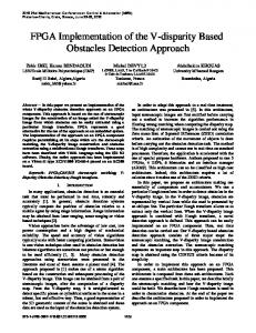
Figure 1: Graph Shows the Point of Intersection of PSNR of Watermark and Embedded Image. The Graph gives Optimized Value of Modulation Index (K) Table 2: The Values of the Embedded Image with the Cover Image. Here the Cover is of Size (256 x 256) Value of K
MSSIM VS Modulation Index 1
Q
NC
1
48.1309
MSSIM 0.998
0.9977
0.9997
MAE 0.9999
5
34.1515
0.9552
0.9515
0.9928
4.9998
10
28.1313
0.8588
0.8581
0.9724
9.9992
15
24.61
0.7556
0.7622
0.9409
14.9975
0.2
20
22.1122
0.6609
0.6738
0.9016
19.9939
0
25
20.1753
0.577582
0.5948
0.8575
24.9874
30
18.5942
0.5053
0.5252
0.8115
29.9142
31
18.31
0.4921
0.5124
0.8022
30.9706
0.8 MSSIM
PSNR
0.6 MSSIM 0.4
1 3 5 7 9 11 13 15 17 19 21 23 25 27 29 31 Modulation Index(K)
Figure 2: Graph shows that Mean Structural Similarity (MSSIM) Index Increases with Increase in Modulation Index (K) From the above tables and graph we come to a conclusion that with the increase of the value of Modulation Index (K) the Quality of the retrieved binary watermark increases. But on the other hand if we increase K, the perceptibility of the embedded image decreases. So we have to make a trade-off between the embedded image perceptibility and the quality of the recovered image.
ISSN 2277 – 503X | © 2012 Bonfring
Bonnfring Internationaal Journal of Advaances in Image Proocessing, Vol. 2, No. 4, December 20012
IV.
ATTACK T IMPLEMENTATION AND D RECOVERY
Various typpes of attack k have beeen used durring im mplementation of the algorithm to test its i robustness to meeasure the errorr from the orig ginal to the exttracted waterm mark thee above mentiooned methodollogies are usedd. The comm mon attaacks along with w JPEG com mpression are listed below in Taable 3 and 4.
4
5.1 Controller The functionality of the contrroller is goverrned by the configuuration registerr. The configuuration registerr is memory mappedd means thaat CPU can write direcctly to the configuuration register.
Table 3: The Vaalue of the Rettrieved Waterm T mark Image witth Original Binary B Waterm mark of the Sizee (64 x 64) Attacks
PSNR
MS SSIM
Q
NC
MAE E
G Gaussian Filter
36.124
0.999 0
0.998
0.9993
0.00002
Gaussian Noise G Saalt and Pepper N Noise Contrast Sttretching
29.134
0.998 0
0.994
0.9968
0.0012
19.689
0.961 0
0.956
0.9729
0.01007
27.093
0.991 0
0.998
0.995
0.0019
Siickle Noise
36.124
0.999 0
0.999
0.9993
0.00002
Shharpened
33.113
0.999 0
0.998
0.9987
0.00004
Table 4: The vaalue of the Retrrieved Waterm T mark Image witth Original Binary B Waterm mark of the Sizee (64 x 64) JPEG attack JPEG90 JPEG60 JPEG50 JPEG30 JPEG20 JPEG10
PSNR Inf 36.124 36.124 33.113 20.326 14.885
MSSIM M 1 0.99 98 0.99 98 0.99 99 0.97 73 0.88 83
Q
N NC
MAE
1 0.9946 0.9946 0.9986 0.9683 0.891
1 0 0.9993 0 0.9993 0 0.9987 0 0.9765 0 0.9179
0 0.0002 0.0002 0.0004 0.0092 0.0324
s tables error implementation and the The above shown ressults of each. The T recovery of the waterm mark image unnder thee influence of the t above errorr is quite well. Here also we can c seee that the moduulation index plays p a vital roole on the amount of recovery of the t original watermark w image and the errror ge. inttrusion in the reecovered imag
F Figure 3(a) shoow the Cover Im mage of Size (256 x 256); Fig 3((b) the Binary Watermark Im mage of Size (64 x 64); Fig 3((c) thee Embedded orr Watermarked d Image; Fig 3((d) the Recoverred Watermaark Image. V.
PROPPOSED VLSI ARCHITECTURE R FOR ENCODER R
The architectture of the pro oposed waterm mark algorithm m is shoown in figuree below. The main buildinng blocks are as folllows: (A) Conntroller (B) Meemory Block (ii) Memory Cover (ii)) Memory Wattermark (iii) Memory M Compaare (C) Assem mbly andd Compare Bloock (D) Code block. b
Figuree 4: The Embeddding Architeccture of the Waatermarking Algorithm m. The configuration is 3bit: 1st Bit (B1) - Softwaare Reset Bit, 2nd Bit (B2) - Preproccess Bit, 3rd Biit (B3) - Start Bit. These 3 bits are used to triggeer 3 consecutivve phases whoose operation is descrribed below. In thhe Software reset phase internnal register is reset r to zero, where the reset is asynchronouss. Here the images are downloaded in covver memory and watermaark memory b (the four respectiively. In Pre-pprocess phase,, b1, b2, b3, b4 bits) seet is calculatedd by reading (88 x 8) byte frrom memory cover and a (2 x 2) bit are read from memorry water in Consecuutive cycles. 64 bit strings are formed as per the Algorithhm in the Asssembly and Compare C block. Result is written in memory coompare. In Staart phase, pixeels bytes are read ouut from Memory Cover sequuentially. In thhis phase the embeddding of the coover image is done by addinng the pixel bytes with w the outpuut of the code block accorrding to the algorithhm. The embeedded image is stored in the t Memory Cover, which is extrracted by the user after thee process is completted. 5.2 Meemory Block The memory coveer is 216 x 17 bits memory which w stores N we have the memory the covver image dataa of 8 bits. Next water which w is 212 x 4 bit long. Heere the watermark image is binary image i which iss represented by b 4 bit. Lastly we have the Memoryy Compare whhich stores 4 bit b compare daata from the assemblly and comparee block. It is 210 x 4bit memoory. 5.3 Asssembly and Coompare Block A decoder is usedd where the sellect line is govverned by 12 bit interrnal register. The T two LSB bits b of registerr are used as the seleect. Depending upon the reegister value and internal strobe each e bit of waatermark data is spawned 16 times and stored in i water_64_ouut which is 6 bit long registter. Now we comparre the water__64_out with the cover_m msb_64_dout which contains c the MSB M plane of thhe cover imagee (8 x 8) non
ISSN 2277 – 503X | © 2012 Bonfring
Bonnfring Internationaal Journal of Advaances in Image Proocessing, Vol. 2, No. 4, December 20012
overlapping blocck. The two 64 6 bit string water_64_out w a and C1, covver_msb_64_ddout is comparred using four comparator (C C22, C3, C4) 16 bit each. The T output of o the individdual com mparator is concatenated and d the compare word is storedd in Meemory Embed. 5.44 Code Block Code block im mplements ± (K X S) as usedd in the proposed alggorithm given in fig. 6. The T code blocck has four PN seqquence generattor S1, S2, S3, S4 and with thhe help of b1, b2, b3, b4, it generattes a value of ±KS. ± K is a 10 bit register. MSB M t sign bit. Neext bit is the in nteger bit and next n 8 bits are for is the fraaction. This K register is memory m mapped to the exterrnal intterface. ±S is a 4 bit signed value v and when multiplied with w K register r the ouutput generates (6+8) bit longg word. The low wer 8 bits b are kept for fraction. If th he operation is perfect, the MSB M of the (6.8) is thee extended sign n bit. The bit next to MSB is the uld have identiical values. Next N siggn bit. These two bits shou fouur bits are forr integer and last l eight bits are for fractiion. Whhen this integeer is added witth (6.8) bit ±KS, decimal poiints hass to be adjustedd for the outpu ut of the transfoorm. VI.
PROPO OSED VLSI ARCHITECTURE R FOR DECODER
The decodinng architecturee of the propposed waterm mark alggorithm is show wn in figure 5. The main buuilding blocks are as follows: (A) Controller C (B) Linear Feedbaack Shift Regisster W Meemory (ii) Memory Embed (D) ( (C)) Memory (i) Watermark Coorrelator.
F Figure 5: The Decoding D Arch hitecture of thee Watermarkingg Algorrithm. 6.11 Controller The controlleer is controlss the flow off the decoder in acccordance to thhe control word d. The controll word is definned by a 2 bit register. The worrking and funnctionality of the t table 4 which w breaks the conntrol word is defined in the funnctionality intoo different phaases. These phaases are triggered by the correspondding bit pattern n of the control word. In Phase1 v and the PN thee four LFSRs are loaded with the seed value seqquence is geneerated. The PN sequences forrmed are storedd in fouur 6 bit registeers. Along witth this data (em mbedded data)) is loaaded in the Meemory Embed is the same phase. p In the next n phase B1, B2, B3, B4 (thee four bits) is i calculated by perrforming correelation between n the sub-blockks and respecttive PN N sequence. The output of the correlator is stored in the Meemory Waterm mark. Data iss extracted froom the Memoory Waatermark throuugh the externaal bus interfacee2 in Phase 3. The T strobe signal iss used for acctivation of the t system. The T
5
m of the decodder gives the detail d of the architecctural diagram control signals providded by the contrroller. Table 5: Thhe control Worrd is given beloow Control C word 01
Statte of operration Phaase I
10
Phaase II
11
Phasse III
Descriptioon (i)LFSR R set (ii)Loadd data in Embedd Memory (i) Decoding Operationn (ii) Ressultant data is stoored in Waterm mark Memory Data reead from Waterm mark Memory
6.2 Linnear Feedback Shift Register The LFSR will bee enabled by the t controller in the Phase w it sets set_seed s = ‘1’’. The seed iss fed by the LFSR when externall interface by the user. The PN (Psseudo Noise sequencce) is generateed using the feeedback mechaanism. In the above stated s algorithm m we used PN sequence of leength 64 bits. Dependding on the polyynomial the LF FSR work in accordance to the tapss to generate thhe PN sequencee. 6.3 Meemory The Memory Embbed is 216 x 17 bits memory which w stores the embbedded image. Next we havee the memory water which is 212 x 1 bit long. Thhe extracted binnary watermarkk image data is storedd in this memoory. 6.4 Correlator In thhis block the correlation c betw ween the embeedded image and the PN sequence is calculated. The method by b which the correlattion is calculatted as the 8 x 8 non-overlappping image block consisting c of 64 6 elements iss taken, each of which is multipliied with corressponding PN sequences s (S1, S2, S3, and S4) whiich are 64 bit long. l The outpuuts are added cumulatively c and thee result is divvided by 64. A comparatorr is used to calculatte whether the outputs are grreater than or less l than the thresholld, if it greaterr than the extrracted bit is 0 else 1. Now by usinng the majorityy logic we deteermine the extrracted bit. If the num mber of ‘1’ iss more than or o equal to eigght then the extracteed bit is ‘1’elsee ‘0’. VII.
RESULLTS
The proposed wattermarking meethodology is based b on the combinnation of chhannel codingg and spreadd spectrum techniquue. We considder a 1 bit/pixxel of size (644 x 64) and 8bits/pixel of size (2256 x 256) binnary images as watermark and thee cover imagee respectively for experimeent purpose. Now, thhe cover imagee is partitioned in (8 x 8) non--overlapping blocks and a the waterm mark image is partitioned in (2 x 2) nonoverlapping blocks. The T partitioninng of the cover i.e. (8x8) mage followedd by the conveersion of the and thee watermark im integer image data to t binary wass done with the help of AB. With the binary b image data d for both thhe partitioned MATLA cover annd the partitionned watermarkk image, we puut them in the test bennch as input cover c and inpput watermark image. The same prrocess in repeated for the deecoding process. After the extraction of the decoded watermarkk image, the annalysis and
ISSN 2277 – 503X | © 2012 Bonfring
Bonfring International Journal of Advances in Image Processing, Vol. 2, No. 4, December 2012
testing of the algorithm is done.
6
Table 6: The Synthesis Results from Xilinx ISE 8.1
The synthesis of the watermark embedding have been implemented on Xilinx (ISE version8.1) based FPGA. We have chosen Virtex series of FPGA to fit the complexities of the design. The device used is xc2vp30-7ff896 for the implementation and the language used is VHDL. The behavioral simulation was done with Synopsys VCS-MX to verify the functionality of the design. A test bench is also written in VHDL to give the input vectors for the simulated program. The estimated power for the proposed architecture is calculated using Xpower of Xilinx 8.1, which comes around 1300 mW and the frequency of operation of the system, is 82.26 M Hz.
Device Utilization Summary Logic Utilization Used Available
Utilization
Number of Slices Number of Slice Flip Flops
959 896
13696 27392
4% 1%
Number of 4 input LUTs
1669
27392
4%
Number of Bonded IOBs
39
416
13%
Number of MULTS 18x18S
1
136
0%
Number of GCLKs
1
16
6%
Table 7: Shows the Results of Extracted Watermark to the Original Watermark for Test Images (256 x 256) with k=20
Table 7: The Results of Extracted Watermark to the Original Watermark for some Test Images The Test Images
Evaluation of the Extracted Watermark to the Original Watermark Normalized Mean Absolute PSNR MSSIM Quality Correlation Error
Airplane
27.092700
0.94663
0.948434
0.993977
0.001953
Baboon
23.819110
0.853293
0.845930
0.987345
0.004150
Barbara
26.123599
0.918701
0.913132
0.992513
0.002441
26.5812
0.92605
0.92527
0.99323
0.0022
33.113300
0.988550
0.993745
0.998490
0.000488
Lena
27.0927
0.95958
0.96553
0.99396
0.00195
Lighthouse
23.1133
0.91431
0.9207
0.98502
0.00488
Pepper
36.1236
0.99739
0.99904
0.99925
0.00024
Boat Cameraman
The Extracted Watermark
Table 8, Gives comparative study of VLSI Architectures of Image Watermarking Systems Proposed in the Literature which shows our Experimental Results have improvement. Table 8: The comparative Study of VLSI Architectures of Image Watermarking Systems Proposed in the Literature Research Work
Multimedia Object Image
Working Domain
Invisible (Binary Watermark)
Image
Transform (Walsh Hadamard Transform)
Chip Statistics Xilinx , Virtex Series XCV50-BG256-6, 50.398MHz Xilinx 14.1, Virtex 4 XC4vlx200-11ff1513, Max. Frequency 90.131 MHz
FPGA platform
Invisible (Binary Watermark)
Image
Spatial and Transform (Dual mode)
Xilinx 14.1, Virtex 4 XC4vlx200-11ff1513, Max. Frequency 90.131 MHz
FPGA platform
Invisible
Image
Maity et. al [19]
Spatial bi-phase Modulation based
Xilinx,Spartan Series XCS-05 ; CLB count = 85 Max. Frequency = 80 MHz
Ghosh et. al [1]
FPGA platform
Invisible (Gray-scale Watermark)
Image
Spatial
Xilinx(ISE version 8.2i),Virtex 4 xc4vlx25-10ff676 Maximum Frequency: 219.542MHz
Ghosh et.al [12]
FPGA platform
Invisible (Gray-scale Watermark)
Image
Spatial
Ghosh et.al [13]
FPGA platform
Invisible (Binary Watermark)
Image
Spatial
Xilinx, Virtex Series xc2vp30-7ff896 power consumption is 650 mw maximum frequency is 82.204 MHz. Xilinx (ISE version8.1) Virtex series (xc2vp30-7ff896) Frequency of operation of the is 82.26 MHz. Estimated Power = 650 mW
Mohanty et. al [14] ,[20] Ghosh et. al [17],[18] Ghosh et. al [16]
Design Type FPGA platform FPGA platform
Watermarking Type Invisible
Spatial
ISSN 2277 – 503X | © 2012 Bonfring
Bonfring International Journal of Advances in Image Processing, Vol. 2, No. 4, December 2012
VIII.
CONCLUSIONS
In this paper we have proposed a spatial domain image watermarking scheme using binary watermark by combined use of channel coding and spread spectrum modulation. The algorithm is simple with low computation cost and can be easily implemented in hardware. Digital design of the proposed algorithm using FPGA has been developed and thus makes it suitable for real time authentication as well as secured communication. The analysis of the watermark image shows with the increase of the value of Modulation Index (K) the Quality of the retrieved binary watermark increases but the perceptual quality of the embedded image degrades. Hence there is a trade off between these two parameters. The VLSI architecture of the Encoder and Decoder had been implemented with Xilinx based Virtex 2pro FPGA and the observations are mentioned. ACKNOWLEDGMENT
[14]
[15]
[16]
[17]
[18]
This work has been partially supported by the SMDP II project, DIT, MCIT, Government of India. REFERENCES [1] [2] [3] [4]
[5] [6] [7] [8]
[9]
[10]
[11]
[12]
[13]
Sudip Ghosh, Pranab Ray, Santi P Maity and Hafizur Rahaman, “Spread Spectrum Image Watermarking with Digital Design”, IEEE International Advance Computing Conference (IACC 2009), Pp.868-873, 2009. Special issue on copyright and privacy protection, IEEE Journal on Selected Areas in Communication (JSCA), 16(4), May 1998. Special issue on enabling security technologies for digital right management, Proceedings of IEEE, 92(6), June 2004. Rui Bao, Tianqi Zhang, Fangqing Tan and Y.E. Wang, "Semi-fragile watermarking algorithm of color image based on Slant Transform and channel coding", Image and Signal Processing (CISP), 2011 4th International Congress on, On page(s): 1039 - 1043 Vol. 2, Pp.15-17 Oct. 2011 I.J. Cox, J. Kilian, T. Leighton, and T. Shamoon, Secure spread spectrum watermarking for multimedia, IEEE Transaction on Image Processing , 6 (12), Pp. 1673-1687, 1997. S.P. Maity, M.K. Kundu and T.S. Das, “Robust SS Watermarking with improved capacity”, Pattern Recognition Letters “Advances in Visual Information Processing”, Elsevier, 28, Pp. 350-357, 2007. S.P. Maity and M.K. Kundu, “A blind CDMA image watermarking scheme in wavelet domain,” Proc. Of IEEE Int. Conf. on Image Proc., Singapore, Pp. 2633-2636, 2004. N.J. Mathai, D. Kundur, and A. Sheikholeslami, Hardware implementation perspectives of digital video watermarking algorithms, IEEE Transaction on Signal Processing, Vol. 51, Pp. 925- 938, April 2003. S.P. Maity , A. Banerjee, A. and M. K. Kundu, VLSI design of Spread Spectrum Image Watermarking—13th National Conference on communications (NCC-2007), Indian Institute of Technology, Kanpur, India, January 26-28, Pp. 251-257, 2007. S.P. Maity , M.K. Kundu and Mrinal K Mandal “Performance Improvement in Spread Spectrum Watermarking via M-band Wavelets and N-ary Modulation”IET International Conference Visual Informal Engineering(VIE 2006), Pp. 35 -40,2006. E. Kougianos, S.P. Mohanty, and R.N. Mahapatra, "Hardware Assisted Watermarking for Multimedia", Special Issue on Circuits and Systems for Real-Time Security and Copyright Protection of Multimedia, Elsevier International Journal on Computers and Electrical Engineering (IJCEE), Vol. 35, No. 2, Pp. 339-358. March, 2009, Sudip Ghosh, Somsubhra Talapatra, Debasish Mondal, Navonil Chatterjee, Hafizur Rahaman and Santi P Maity, “VLSI Architecture for Spatial Domain Spread Spectrum Image Watermarking using GrayScale Watermark”, in 16th International Symposium on VLSI Design and Test (VDAT, 2012) from 1-4 July 2012 at Bengal Engineering and Science University, Shibpur, India. Pp. 375-376 (Springer, LNCS),2012. Sudip Ghosh, Somsubhra Talapatra, Debasish Mondal, Navonil Chatterjee, Hafizur Rahaman and Santi P Maity, “VLSI Architecture for
[19] [20] [21]
7
Spread Spectrum Image Watermarking using BinaryWatermark” in IEEE, International Conference on Advances in Computing and Communications(ICACC), from 9-11August 2012 at Rajagiri School of Engineering & Technology, Cochin, Kerala, India, Pp.166-169, 2012. Saraju P. Mohanty, C. Renuka Kumara and Sridhara Nayak, “FPGA based implementation of an invisible-robust image watermarking encoder” Intelligent Information Technology, Lecture Notes in Computer Science Vol. 3356, Pp. 344-353, 2005. A. Basu, T.S. Das, S. Maiti, N. Islam and S.K. Sarkar, “FPGA based implementation of robust spatial domain image watermarking algorithm”, 4th International Conference on Computers and Devices for Communication, CODEC ,Pp 1–4, 2009 Sudip Ghosh, Somsubhra Talapatra, Jayasree Sharma, Navonil Chatterjee, Hafizur Rahaman and Santi P Maity, “Dual Mode VLSI Architecture for Spread Spectrum Image Watermarking using Binary Watermark” in 2nd International Conference on Communication, Computing & Security (ICCCS-2012) from 6-8 October 2012 at National Institute of Technology Rourkela, India.Pp.784-791, 2012. Sudip Ghosh, Somsubhra Talapatra, Santi P Maity and Hafizur Rahaman “A Novel VLSI Architecture for Walsh-Hadamard Transform” in IEEE 2nd Asia Symposium on Quality Electronic Design (ASQED-2010) from 3-4 August, 2010 at Penang, Malaysia. Pp. 146 – 150, 2010. Sudip Ghosh, Somsubhra Talapatra, Sudipta Chakraborty, Navonil Chatterjee, Hafizur Rahaman and Santi P Maity, “VLSI Architecture for Spread Spectrum Image Watermarking in Walsh-Hadamard Transform Domain using Binary Watermark” in 3rd IEEE International Conference on Computer and Communication Technology ( ICCCT 2012) from 23-25 November 2012, at Motilal Nehru National Institute of Technology(MNNIT), Allahabad, India. Pp. 233-238, 2012. S.P. Maity, A. Banerjee and M.K. Kundu“An Image-inImagecommunication scheme and VLSI implementation using FPGA”,INDICON 2004, IIT Kharagpur, India. Pp.6-11, 2004. S.P. Mohanty, E. Kougianos and N. Ranganathan, “VLSI architecture and chip for combined invisible robust and fragile watermarking”,IET Computers & Digital Techniques (CDT) 1(5) Pp. 600-611, 2007. Z. Wang, A.C. Bovik, H.R. Sheikh and E.P. Simoncelli, "Image quality assessment: From error visibility to structural similarity,"IEEE Transactions on Image Processing, Vol. 13, No. 4, Pp. 600-612, Apr. 2004.
Sudip Ghosh was born at Kolkata, West Bengal, India in the year of 1977. He received his B.E. in Electronics and Communication Engineering from Sikkim Manipal Institute of Technology, Sikkim, India in the year 2001 and M.S. in VLSI CAD from Manipal Centre of Information Science (MCIS),Manipal, India, in the year of 2005.He completed his B.E. project at VECC(Variable Energy Cyclotron Centre ), kolkata(under DAE (Department of Atomic Energy , Govt. of India). After his B.E. he worked at Saha Institute of Nuclear Physics, Kolkata,India at Microelectronics division (Govt. of India) and also done his M.S. project at Indian Statistical Institute (ISI), Kolkata at Advanced Computing And Microelectronics Unit(ACMU) (Govt. of India).He is a member of CSI(Computer Society of India) and VSI (VLSI Society of India). Currently he is working as an Assistant Professor at School of VLSI Technology, Bengal Engineering And Science University, Shibpur.(BESUS), Howrah, India and also actively doing his research at BESUS. His area of specialization includes Synthesis of Digital Systems, Digital VLSI architectures, VLSI Testing and Verification and Digital Watermarking of Image and Video signals.(E-mail:
[email protected]) Santi P. Maity is working as Associate Professor in the Department of Information Technology, BESU, Shibpur, India. During January, 2009 to July, 2009 and February, 2011 to July, 2011 he did post-doctoral research work in Laboratoire des Signaux et Systems, Supelec, France. His research areas include digital image watermarking, multi-user detection in CDMA, digital signal processing, digital wireless communication, VLSI watermarking. He has contributed about 100 research papers.
ISSN 2277 – 503X | © 2012 Bonfring
Bonfring International Journal of Advances in Image Processing, Vol. 2, No. 4, December 2012
Hafizur Rahaman (IEEE SM'10) received the Bachelor of Electrical Engineering degree from Calcutta University, India, in 1986, the Master degree in Electrical Engineering and Ph.D. (Computer SC. & Engg.) degree from the Jadavpur University, Calcutta, India, in 1988 and 2003 respectively. He served CMPD Institute (R & D organization), India, from 1988 to 1995. He served as a faculty member at India Institute of Information Technology-Calcutta (IIIT-C), India, from 1995 to 2003. Since 2003, Dr. Rahaman has been on the faculty of the Bengal Engineering and Science University, Shibpur, India, where he is full professor. Dr. Rahaman has contributed to very large scale integrated computer-aided design and test, design and test of Micro-fluidic biochips and emerging nanotechnologies with major publications in journals and conferences, spanning more than 15 years. He has published more than 140 research articles in archival journals and refereed conference proceedings. Dr. Rahaman visited as Post Doctoral Research Fellow under EPSARC Grant at the department of Computer Science, Bristol University, UK, during 2006– 2007. During 2008–2009, Dr. Rahaman received Royal Society International Fellowship Award to carry out one year advanced research in the Design and Verification Division of Computer Science Department, University of Bristol, United Kingdom. He leads the VLSI design and test group at the Bengal Engineering and Science University, Shibpur, India. He is the principal coordinator of the department of Information Technology (DIT), MCIT, Govt. of India funded SMDP-II research project at Bengal Engineering and Science University, Shibpur, India. Dr. Rahaman is a Member of the VLSI Society of India (VSI), the IEEE, the IEEE Computer Society, and ACM Sigda. He served on the conference committees of the International Conference on VLSI Design, the VLSI Design and Test Workshop (VDAT), Asian Test symposium (2005), ISED (2010, 2012).
ISSN 2277 – 503X | © 2012 Bonfring
8