Image sensor array based on graphene-CMOS integration AUTHORS: STIJN GOOSSENS1, †, GABRIELE NAVICKAITE1, †, CARLES MONASTERIO1, †, SHUCHI GUPTA1, †, JUAN JOSÉ PIQUERAS1, RAÚL PÉREZ1, GREGORY BURWELL1, IVAN NIKITSKIY1, TANIA LASANTA1, TERESA GALÁN1, ERIC PUMA1, ALBA CENTENO3, AMAIA PESQUERA3, AMAIA ZURUTUZA3, GERASIMOS KONSTANTATOS1,2,*, FRANK KOPPENS1,2,* AFFILIATIONS: 1 ICFO-Institut
de Ciencies Fotoniques, The Barcelona Institute of Science and Technology, 08860 Castelldefels (Barcelona), Spain. 2 ICREA
– Institució Catalana de Recerça i Estudis Avancats, Barcelona, Spain.
3Graphenea
SA, 20018 Donostia-San Sebastian, Spain
*Correspondence to:
[email protected] ,
[email protected] † These authors contributed equally to this work
ABSTRACT: Integrated circuits based on CMOS (complementary metal-oxide semiconductors) are at the heart of the technological revolution of the past 40 years, as these have enabled compact and low cost micro-electronic circuits and imaging systems. However, the diversification of this platform into applications other than microcircuits and visible light cameras has been impeded by the difficulty to combine other semiconductors than silicon with CMOS. Here, we show for the first time the monolithic integration of a CMOS integrated circuit with graphene, operating as a high mobility phototransistor. We demonstrate a high-resolution image sensor and operate it as a digital camera that is sensitive to UV, visible and infrared light (300 – 2000 nm). The demonstrated graphene-CMOS integration is pivotal for incorporating 2d materials into the next generation microelectronics, sensor arrays, low-power integrated photonics and CMOS imaging systems covering visible, infrared and even terahertz frequencies.
1
INTRODUCTION The immense impact of microelectronics on our society is accredited to the miniaturization of silicon integrated circuits1,2. Alongside faster CPUs and higher capacity memories, it has enabled low-cost and high-performance digital imaging3, with stunning pixel densities above 100 megapixels per chip4,5. More recently, the integration of photonics with CMOS electronic circuits is paving the way to large
data communications bandwidths, higher connection capacities, and on-chip optical interconnects6. However, the difficulty in integrating nonsilicon electro-optical materials with silicon integrated circuits has been a serious impediment to unlock its vast potential for imaging beyond the visible range, on-chip low-power optical data communications and compact sensing systems. Graphene and
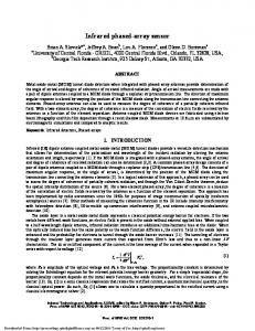
Fig. 1 Back-end-of-line (BEOL) CMOS integration of CVD graphene with 388 x 288 pixel image sensor read-out circuit. a) 3d impression of the CVD graphene transfer process on a single die containing an image sensor read-out circuit that consists of 388 x 288 pixels. b) Side view explaining the graphene photoconductor and the underlying read-out circuit. The graphene channels are sensitized to UV, visible, near infrared and short wave infrared light with PbS colloidal quantum dots: upon light absorption an electron-hole pair is generated, due to the built in electric field the hole transfers to the graphene while the electron remains trapped in the quantum dots. The schematic represents the CTIA based balanced read-out scheme per column and global correlated double sampling stage and output driver. c) 3d impression of the monolithic image sensor displaying the top level with graphene carved into s-shaped channels sensitized with a layer of quantum dots, vertical interconnects and underlying CMOS read-out circuitry. d) Photograph of the image sensor indicating the functionality for each area. To enhance contrast for different regions the photograph was taken before the colloidal quantum dots were deposited. Inset 1: Microscope image of the lower right corner of the active area of the ROIC. Inset 2: scanning electron micrograph of the active area of the image sensor displaying the s-shaped graphene channels. Both images were taken before the quantum dots were deposited.
2
related 2d materials have shown their merits for a wide range of optoelectronic 7 applications , such as data 8–10 communications , high-performance 11 LEDs , ultra-fast optical modulation12 and photodetection with speeds up to 80GHz13 and extreme broadband photodetection14– 21, for UV, visible, infrared and terahertz. Also, several high performance electronic devices and sensors have been demonstrated, such as ultra-sensitive Hall sensors22,radio frequency receivers23, strain sensors24, biosensors25, gas sensors26, and high frequency transistors27,28. However, for these lab demonstrations, separate instruments performed the read-out. In order to unlock the true potential for these application areas, monolithic integration of 2d materials with CMOS integrated circuits is required as it enables compact and low-cost devices.
realization of an image sensor with a 388x288 array of graphene-quantum dot photodetectors that is operated as a digital camera with high sensitivity for both visible and short-wave infrared light. The ~110,000 photoconductive graphene channels, are all individually integrated vertically, connecting to the individual electronic components of a CMOS readout integrated circuit (ROIC). The chip containing the circuitry is similar to those used for commercial image sensors in digital cameras3, commonly used in smartphones, but here operating for both visible and short-wave infrared light (300 – 2000 nm). This wavelength range is so far not attainable with monolithic CMOS image sensors. Therefore, a broadband sensing platform that is monolithically integrable with CMOS is highly desirable. This proof-ofprinciple monolithic CMOS image sensor is a milestone for low-cost and high-resolution broadband and hyperspectral imaging systems32, with applications in safety and security, smartphone cameras, night vision, automotive sensor systems, food and pharmaceutical inspection, and 33 environmental monitoring .
One of the key advantages of 2d materials is that they can be transferred to virtually any substrate, and is therefore a key enabler for monolithic integration with silicon integrated circuits based on CMOS. This permits strong benefit from the technological maturity and time/cost effectiveness of CMOS wafer-scale production processes and the rapid developments of wafer-scale chemical vapour deposition (CVD) growth and transfer of graphene23,29–31. Here we integration integrated integration
DEVICE STRUCTURE AND FUNCTIONALITY The integration of our CMOS graphenequantum dot image sensor is a back-end-ofline (BEOL) process schematically shown in Fig. 1a. The process starts with a graphene transfer on a CMOS die that contains the read-out circuitry of the image sensor. Now, each pixel structure is covered with a layer of graphene that is connected with the bottom readout circuitry through vertical metal interconnects (Fig. 1b and c). Next,
present the first monolithic of graphene with a CMOS circuit. In this case, the potential is shown by the 3
graphene is patterned to define the pixel shape as is shown in Fig. 1d, inset 2 and Supplementary Figure S1. Finally, a sensitizing layer of PbS colloidal quantum dots is deposited via a simple spin-casting process, on top of the graphene layer. The photoresponse is based on a photogating effect as follows16,17 light is absorbed in the quantum dot layer followed by transfer of photo-generated holes (or electrons) to the graphene, where these circulate due to a bias voltage applied between the two pixel contacts (illustrated in Fig. 1b). Therefore, the photo-signal is sensed as a change in the conductance of the graphene transport layer. Due to the high mobility of graphene (here ~1000 cm2/Vs), this photoconductor structure exhibits ultra-high gain of 108 and responsivity above 107 A/W, which is a strong improvement compared to photodetectors and imaging systems based on quantum dots only34. Our individual photodetector prototypes show detectivity above 1012 cm∙√Hz/W (Jones) and spectral sensitivity from 300-2000 nm, and together with recently demonstrated switching times of 0.1-1ms clearly validate the applicability for infrared imaging35. Apart from the array of photosensitive pixels, the imager contains a row of blind pixels that are used to subtract the dark signal as the photodetectors are voltage biased. We remark that here, the spectral range is determined by the quantum dot material and size, but this approach can be generalized to other types of sensitizing materials in order to extend or tune the spectral range of the sensor element.
The functional elements of the CMOS circuitry are shown in Fig 1b, c and d. The elements surrounding the active pixel area provide multiple functions: signal path control, photodetector biasing, tuneable compensation resistors, blind pixels, amplification and read-out of the photosignal from pixel to output, and control of the image exposure and shutter operation. The photosignal per pixel is acquired through a balanced read-out scheme as shown in the schematic in Fig 1b, that consists of the blind pixel (with resistance Rblind) and a tuneable compensation resistance Rcomp in series with the pixel resistance Rpixel that can be digitally controlled for each individual pixel. Pixels are addressed sequentially on a row-by-row basis (rolling shutter) with a frame rate of maximally 50 frames per second (fps). The signal readout chain (see Fig. 1b and Supplementary Figure S5) is based on a Capacitive Trans-Impedance Amplifier (CTIA) per column that integrates the current difference between photosensitive and blind pixels. The amplifier output is sampled, before and after exposure, in a storage block, also per column, and all column signals are multiplexed into a common output bus terminal. Finally, a correlated double sampling (CDS) correction is performed to reduce readout noise and the resulting output signal Vout is sent to the imager’s analogue output.
4
DIGITAL CAMERA We first present the main results of our work in Fig. 2, which encompass several types of images that have been captured with our prototype digital camera comprising the graphene-CMOS image sensor. The configuration for obtaining these images is schematically illustrated in Fig. 2a: the graphene-QD image sensor captures reflection images from objects illuminated by a light source of visible or short-wave infrared light. The grey scale plots of Fig. 2 are compiled of the normalized
photosignals for each of the photodetection pixels of the 388 x 288 array, amplified and multiplexed by the CMOS integrated circuit. Not the entire active area of the image sensor is covered with graphene due to the finite size of the CVD graphene sheet and manual alignment of the transfer (see Supplementary Notes and Figure S7); the pixels that were not covered with graphene and hence did not show any conductance are represented as continuous grey areas. The image shown in Fig. 2c has been obtained using an image sensor with
Fig. 2 Hybrid graphene and colloidal quantum dot based image sensor and digital camera system a) Digital camera setup representation: the image sensor plus lens module captures the light reflected off objects that are illuminated by an external light source. Supplementary Figure S3 contains all the details of the image capturing setup for each of the images in this figure. b) Near infrared (NIR) and short wave infrared (SWIR) light photograph of an apple and pear. An incandescent light source (1000W, 3200K) illuminated the objects. As this image sensor is sensitive to visible (VIS), NIR and SWIR light (300-1850 nm, Figure 4b) we placed an 1100 nm long pass filter in the optical path to reject all light that a conventional Si-CMOS sensor can capture. The axis tick labels indicate the column (horizontal axis) and row (vertical axis) numbers. The illumination yielded an irradiance on the image sensor of ~1·10-4 W/cm2. The grey scale represents the photosignal dV in volts (dV=Vout,light- Vout,dark, Supplementary Methods) normalized to dV obtained from a white reference image. An image processing scheme as described in the Supplementary Methods has been performed. c) VIS, NIR and SWIR photograph of a box of apples, illuminated with the same source as in b), but without the 1100nm long pass filter. d) VIS and NIR (this image sensor is sensitive to 300-1000 nm, Figure 4a) photograph of standard image reference ‘Lena’ printed in black and white on paper illuminated with an LED desk lamp. e) NIR and SWIR image of a rectangular block covered in fog as shown in f). The same source as in a) illuminated the scene. g) NIR and SWIR image of a rectangular block behind a silicon wafer as shown in h). The same source as in a) illuminated the scene. i) NIR and SWIR image of a glass of water as shown in j). The same source as in a) illuminated the scene. A smartphone camera captured images f), h) and j) under similar lighting conditions..
5
quantum dots that have an exciton peak at 920 nm, corresponding to the peak absorption of the quantum dots as measured in solution. The objects were illuminated with visible light with illumination power of ~1·10-4 W/cm2, which corresponds to office illumination conditions. We remark that a reasonable fraction of the pixels was sensitive to much lower light levels (further discussed below), but the pixel drift and spread in sensitivity were too large to obtain extreme low-light level images. Further optimization of the fabrication process and wafer-scale processing can resolve these nonuniformities. The images shown in Fig 2 b,d,e,g,i have been obtained using an image sensor with CQDs that have an exciton peak at 1670 nm. For the image in Fig 2 b,e,g,i we illuminated the objects with an incandescent light source and filtered all the visible light from