Feb 6, 2008 - Temporary drift of the receive data stream is absorbed by a pro- grammable ... ly drive the flip-flops as well as a multiphase CML XOR phase detector ... [3] H. Partovi, W. Walthes, L. Ravezzi et. al, âData Recovery and Retiming.
Please click on paper title to view Visual Supplement. ISSCC 2008 / SESSION 25 / BUILDING BLOCKS FOR HIGH-SPEED TRANSCEIVERS / 25.6 25.6
A 1.8W 115Gb/s Serial Link for Fully Buffered DIMM with 2.1ns Pass-Through Latency in 90nm CMOS
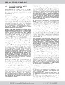
Dirk Pfaff, Sivakumar Kanesapillai, Volodymyr Yavorskyy, Carlos Carvalho, Reza Yousefi, Muhammad Ali Khan, Trevor Monson, Mark Ayoub, Claus Reitlingshoefer Diablo Technologies, Gatineau, Canada Bandwidth and capacity of memory systems based on commodity DIMM are limited by the parallel stub bus between the modules and the memory controller. As a result, the maximum number of DIMMs per channel has to be reduced with the market entrance of every new DRAM generation. Fully buffered DIMMs (FBDIMM) eliminate this limitation by replacing the parallel stub bus by a serial point-to-point link with a repeater device (advanced memory buffer (AMB)) residing on every FBDIMM. While solving the bandwidth-capacity problem, FBDIMM systems potentially increase the memory latency. Keeping the pass-through latency below 3ns, combined with careful command sequencing [1], alleviates the latency problem. Another challenge associated with FBDIMM is the high power consumption of the AMB. Current AMBs tend to consume more than 8W [2] with the high-speed serial link alone dissipating 4W [3]. Minimization of AMB power consumption, and most prominently its high-speed serial link delivering up to 115Gb/s, remains a critical undertaking to the delivery of high-bandwidth and high-capacity memory systems. In this paper, a low-latency low-power high-speed serial link for FBDIMM is reported. Figure 25.6.1 shows a block diagram of the link. A total of 24 transceivers, each running at 4.8Gb/s, form the core of the link which is completed by a CMU. Referring to Fig. 25.6.1, each transceiver features a quarter-rate receive front-end and a quarter-rate transmit backend. Standard CMOS logic performs receive de-multiplexing and transmit multiplexing. Temporary drift of the receive data stream is absorbed by a programmable elastic buffer (FIFO). Re-timed receive data is directly forwarded to the transmit multiplexer in pass-through mode. The CMU generates single phase clocks that are delivered to the transceivers by shielded transmission lines. Transmit clock pulses can be swallowed as required to align data to the digital core. Referring to Fig. 25.6.2, a fully differential PLL and a split regulated supply provide high noise immunity. Programmable 8-to33MHz loop bandwidth enables minimization of the reference clock phase noise. As shown in Fig. 25.6.2, a feedback multi-pass ring oscillator is engaged. Besides a wider tuning range compared to a conventional feed-forward multi-pass structure, the feedback multi-pass topology endows the oscillator with a more constant voltage swing over the tuning range. Figure 25.6.2 reveals a simplified schematic of the CML delay cell. Tuning is achieved by altering the tail currents that are mirrored from a source degenerated gm stage driven by the differential tuning voltage. Figure 25.6.3 outlines the receiver featuring a multiphase PLL with programmable phase shift [4]. Trimmable ground-referred 50Ω termination resistors deliver a scaled version of the receive signal to a folded cascode stage that converts the input signal to a VDD-referred signal. High receiver sensitivity necessitates 18dB voltage gain, which is delivered by 3 differential gain stages. DC offset is compensated by the injection of a programmable current into the folded cascode load. Switches at the receiver input facilitate DC-offset calibration. Five CML flip-flops latch the data and deliver 4 quarter-rate data streams and an edge bit stream. The latter is used to form an Alexander phase detector serving a digital dual-loop CDR circuit. A ring oscillator of the same topology used in the CMU generates 8 equidistant clock phases that directly drive the flip-flops as well as a multiphase CML XOR phase detector [4]. In order to improve phase linearity, the phase detector is segmented into 36 parallel units with each unit containing
462
two combined XOR gates, shown in Fig. 25.6.3. Nine current sources are available to bias 9 XOR gates through a switch fabric while the other gates remain disabled. The decoder logic controlling the switch fabric facilitates linear phase shifts in 6.1ps steps. The combined XOR currents are steered into a differential loop filter incorporating a common-mode feedback loop. Figure 25.6.4 shows the transmitter featuring a single post-cursor equalizer. CML buffers are used to drive the load for reduced noise generation. In order to accommodate 6 amplitudes and 4 equalization levels, the driver is segmented into 90 identical units. Each segment can be driven either by the rail-to-rail cursor or post-cursor data steam. Alternatively, each segment can be used to lift the output common mode. The remaining transmitter section, implemented in differential CMOS for reduced power consumption, multiplexes skewed quarter rate data streams into a full rate cursor and post-cursor data stream. Figure 25.6.4 outlines the timing. Multiplexing is performed by differential transmission gates, realized by NMOS pass transistors followed by PMOS level restorers. The transmission gates are controlled by AND combinations of quarter-rate quadrature clocks that themselves are generated by a quadrature divider driven from the half-rate transmit clock. A fabricated AMB chip incorporating the described high-speed link supports error-free operation at 4.8Gb/s transceiver data rate in various FBDIMM memory systems. The rms jitter of the half-rate transmit clock is measured as 2ps by integration of the phasenoise spectral density in a 100kHz to 1GHz band. A phase-noise plot, measured at the transmitter output, is shown in Fig. 25.6.5. The same figure shows a PRBS7 630mVppdiff transmit eye diagram. Eye height and opening comply with the specifications for FBDIMM [5]. The BER of the receiver versus phase of an applied PRBS31 input signal is shown in Fig. 25.6.6. The resulting bathtub curve, measured with the CDR disabled, exhibits a 0.6UI wide opening at BER=1e-12. This is confirmed by a jitter-tolerance test shown in Fig. 25.6.6 as well. The rms random jitter of the receiver can be derived from the slope of the bathtub curve at low BER as 2.6ps. Receiver sensitivity is measured as 50mVppdiff over a wide range of common-mode input levels. Besides PRBS31, the receiver is exposed to a standard compliant minimum pulse [5] that can be captured with BER=1e-12 over a 0.2UI wide phase range, as indicated by the narrow bathtub curve shown in Fig. 25.6.6. The 3dB bandwidth of the CDR circuite is measured by sinusoidal modulation of the input data and observation of the recovered clock through a sampling scope. The bandwidth varies with the data pattern, but stays within a measured 200kHz to 350kHz range. The lower bandwidth limit is reached with a minimum transition data pattern featuring 500 consecutive identical bits. Measured from receive package ball to transmit package ball, the passthrough latency is 2.1ns with 300ps receive data drift being applied. Higher drift absorption can be configured at the cost of increased latency. Finally, the entire link consumes 1.74W from a 1.0V supply with all transceivers running at 4.8Gb/s, yielding 15mW/Gb/s power consumption. The chip can withstand 2kV HSM and 500V CDM ESD surges; a die micrograph is shown in Fig. 25.6.7. References: [1] B. Ganesh, A. Jaleel, D. Wang and B. Jacob, “Fully-Buffered DIMM Memory Architectures: Understanding, Mechanisms, Overhead and Scalings,” IEEE Int. Symp. On High Performance Computer Architecture, pp. 109-120, Feb. 2007. [2] Intel, “Intel 6400/6402 Advanced Memory Buffer Datasheet,” Datasheet, pp. 38-42, Dec. 2006. [3] H. Partovi, W. Walthes, L. Ravezzi et. al, “Data Recovery and Retiming for the Fully Buffered DIMM 4.8Gb/s Serial Links,” ISSCC Dig. Tech. Papers, pp. 336-337, Feb. 2006. [4] T. Toifl, C. Menolfi, P. Buchmann, et al., “A 0.94-ps-RMS-jitter 0.016mm2 2.5-GHz Multiphase Generator PLL with 360° Digitally Programmable Phase Shift for 10-Gb/s Serial Links,“ IEEE J. Solid State Circuits, vol. 40, pp. 2700-2712, Dec. 2005. [5] “FB-DIMM High Speed Differential PTP Link at 1.5V – Specification,“JEDEC, Dec. 2005.
• 2008 IEEE International Solid-State Circuits Conference
978-1-4244-2011-7/08/$25.00 ©2008 IEEE
Please click on paper title to view a Visual Supplement.
Please click on paper title to view Visual Supplement. ISSCC 2008 / February 6, 2008 / 10:45 AM
Figure 25.6.1: High-speed link block diagram and transceiver architecture.
Figure 25.6.2: CMU block diagram, ring-oscillator topology and delay-cell schematic.
Figure 25.6.3: Receiver incorporating a multiphase PLL with programmable phase shift.
Figure 25.6.4: Transmitter schematic and principal timing diagram.
25
Figure 25.6.5: Transmit clock phase noise (top) and transmit eye diagram (bottom).
Figure 25.6.6: Receiver bathtub curves (top) and sinusoidal jitter tolerance plot (bottom).
Continued on Page 628
DIGEST OF TECHNICAL PAPERS •
Please click on paper title to view a Visual Supplement.
463
Please click on paper title to view Visual Supplement. ISSCC 2008 PAPER CONTINUATIONS
Figure 25.6.7: Advanced memory buffer die micrograph.
628
• 2008 IEEE International Solid-State Circuits Conference
978-1-4244-2011-7/08/$25.00 ©2008 IEEE
Please click on paper title to view a Visual Supplement.