Muhammad Nouman Qaiser, Muhammad Usama, Bilal Ahmad, Muhammad Ali Tariq and Hassan Abbas. Khan. Department of Electrical Engineering, Lahore ...
Low Cost, Robust and Efficient Implementation of MPPT based Buck Boost Converter for Off-grid PV Applications Muhammad Nouman Qaiser, Muhammad Usama, Bilal Ahmad, Muhammad Ali Tariq and Hassan Abbas Khan Department of Electrical Engineering, Lahore University of Management Sciences, Lahore, 57792, Pakistan Abstract
-
Rapidly growing solar PV energy sector demands
development of low cost, reliable and energy efficient systems to continue its growth globally. Most PV systems deployed in the developed countries are based on grid-tied topology as the grid in these countries is largely stable. However, most of the developing world has an intermittent grid or a bulk of the population is not connected to the grid in the first place. In this context, this paper proposes a design and implementation of a low cost, efficient and robust maximum power point tracking based charge controller suited for stand-alone or backup PV applications. The charge controller incorporates a buck-boost topology that ensures a continuous
battery
implementation
charging
includes
a
in
various
hardware
conditions. protection
The against
breakdown of converter switches in addition to a software based protection software
approach
algorithm,
derived all
from
programmed
converter into
a
analysis. low cost
The
8 bit
microcontroller, also incorporates a three state charging capability to charge battery under optimal conditions. The designed system was tested at 150W (output power) and performed optimally.
Index Terms
-
efficiency which can be overcome by employing more efficient controlled switches [6, 7] . The improved efficiency comes at the cost of additional control requirement which is hardly a concern due to a complementary switching scheme. The inherent ability to utilize a higher or lower panel voltage to charge batteries makes it an ideal choice for various irradiance conditions and wide variety of panels. The bidirectional nature of converter requires that it is controlled intelligently to prevent any reverse power flow. This has been overcome through converter analysis shown in the next section. It should be noted that for this application we do not require reverse power flow however there are various other applications in DC micro and nano-grids which require reverse power flow and thus this converter design could be highly beneficial for such implementations.
PV system, MPPT, Buck-Boost and battery
charging.
I.
INTRODUCTION
Increasing power requirements and high cost of fossil fuels have resulted in an acute shortage of energy, especially in developing countries. The demand for renewable energy resources has therefore grown significantly over the last decade[I]. Efficient utilisation of environmentally friendly, sustainable and affordable energy resources has become a critical need in the current circumstances. Solar PV based applications are generally most pertinent to distributed generation in locations where the grid is unavailable or unreliable [2]. In this topology, the energy extracted from PV panels is either used to charge batteries or to drive loads directly in the case of surplus production. The most critical component in this regard is a charge controller that can extract optimum power from the panel(s) through 'dynamic searching' of the maximum power point[3].
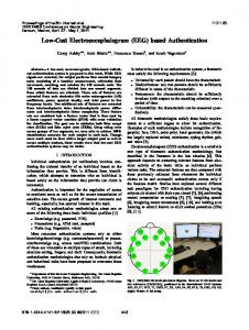
Figure i: Buck-Boost Converter topology with two controlled switches using 8 bit microcontroller
II. METHADOLOGY Traditionally, battery backed up systems employ buck converters based charge controllers due to simple implementations [4,5]. For a general buck converter,the output voltage (Vout) given in terms of input voltage (Vin) is given as: Vout = D. Vin where D is the duty cycle of the switching element. However, in this work, we employ a buck-boost converter topology employing two controlled switches instead of a diode and a switch. The lossy nature of power diodes (in conventional Buck-Boost topology) put a limit to converter's
978-1-4799-4398-2/14/$31.00 ©2014 IEEE
The converter topology used in this work is illustrated in figure 1. The converter presented is a variant of a few existing buck boost converter topologies [8] . This particular topology is a two switch synchronous converter with inductor functioning as the primary energy storage element. The topology imparts a few benefits and limitations as described in the later sections. Provided that the limitations are well addressed, the converter allows for a simplified control, enhanced efficiency and a
3701
synchronous nature which makes it very suitable for DC to DC conversion applications and there well suited to applications like maximum power point tracking. The converter starts perturbing duty cycle from a value that would result in a positive charging current at all times. Three state battery charging has been achieved by carefully monitoring maximum charging current and battery terminal voltage during charging. The third state of charging initiates when the battery has remained on constant voltage charge and the charging current value has dropped to less than 10% of the maximum allowable value. A.
(I)
VL = Vbat
During the interval (I-D), Q2 turns on and Ql is off, Hence: (2) VL = -Vpanel Where, V L is the voltage across inductor. The average voltage across the inductor is zero (in steady state) and therefore it can be written as: < VL > = D. Vbat +
[(1
-
D). -Vpanet l
= 0
(3)
The conversion ratio M(D) of the buck boost converter is therefore given as:
Converter Analysis
The improved efficiency comes at a cost of more complicated control strategy for the converter. It is therefore imperative that critical limits for allowable duty cycle must be assessed and implemented for its use. In order to carry out a CCM analysis of the converter, the converter is considered lossless (for simplicity). For convention,switch Ql closes for the duty ratio D, and Q2 for I-D. The provided analysis is perfonned under steady state conditions. In a qualitative explanation,during the instance (I-D) the upper switch (Q2) turns on and causes a current to buildup in the inductor. During this stage both the input capacitor and panel supply current that flows through the inductor. During instance D, Q 1 turns on and current tries to continue flow through the inductor while decreasing in magnitude. This flow of current follows a loop shown in figure 2 and charges the battery. In this interval, the panel continues to supply current charging the input capacitor.
�
OJ
C
Q2
rn a....
+
�
Q1
VL
=
-Vpanel
Fizure 3: Converter state durinz J -D (low PWM lozic level)
MeD) OJ
C�__-I
T
rn
a.... �,....... .
1
=
Vpanel Vbat
=
...E... 1-D
(4)
The switching frequency of 100 KHz was chosen to minimize size of energy storage elements (inductor and capacitors) in the converter. In theory, the converter (in two switch topology) allows bi-directional flow of power between sources. However, the converter could have also been designed using a single controlled switch and another unidirectional un-controlled switch (power diode) but this would have lowered the overall efficiency due to higher forward voltage drop in power diodes (� 1 V). The proposed 'two switch topology' demands that the switches be switched in a complementary fashion which largely simplifies the control aspect. The converter is driven by a single PWM source interfaced to a complementary boot strapped half bridge gate driver. Hence the use of both controlled switches enhances efficiency at a lower cost without adding considerable difficulty in control aspect.
Fizure 2: Converter state durinz D (hizh PWM lozic level)
During the interval D, Q 1 is on and Q2 is off,hence:
978-1-4799-4398-2/14/$31.00 ©2014 IEEE
3702
B.
Battery Charging
Icharging + Vint
•
-re .. �
V bat
�
:= [
Simplifying further,the following condition is obtained: The model of battery used in is further calculations illustrated in figure 4. Vbat is the terminal voltage for the battery whereas Vint the internal voltage of the battery cells illustrated as shown. At any point, the charging current for the battery is:
Figure 4: Battery Model
[charging
=
Vbat-Vint R.mt
(5)
By substituting Vbat from this equation into (4),we get: Vpanel =
D 1-D
. ( Icharging Rint + Vint )
[Charging
=
(1-D) .Vpanel
D max
Vpanel Vpanel+Vint
(9)
This restriction on the duty cycle enables the microcontroller to determine the condition for a positive charging current. When the converter is disabled (or more precisely the gate driver is disabled so both switches are turned oft),VintCan be determined as it is equal to V bat (no current flowing). Before enabling the gate driver, the panel voltage and battery terminal voltage is sensed and Dmax calculated for a positive charging current. In general batteries have a very small internal resistance and therefore can draw current beyond there safe limits during charging causing battery heating and gassing [9]. This is avoided by a constant current charging stage whereby charging current is held constant at a maximum value depending on the
(6) (7)