capacitive crosstalk noise has been a well known factor that causes interconnect delay variation. Nano-meter technology regime has pushed inductive coupling ...
IEEE 2006 Custom Intergrated Circuits Conference (CICC)
Measurement of Inductive Coupling Effect on Timing in 90nm Global Interconnects Yasuhiro Ogasahara, Masanori Hashimoto, and Takao Onoye Dept. Information Systems Engineering, Osaka University, Suita 565-0871, JAPAN {ogshr,hasimoto,onoye}@ist.osaka-u.ac.jp strong
Abstract— Inductive coupling is becoming a design concern for global interconnects in nano-meter technology. This paper shows measurement results of inductive coupling effect on timing, and reveals that inductive coupling noise is a practical design issue in 90nm technology. The measured delay change curve is consistent with circuit simulation results with RLC interconnect model, and definitely different from those of conventional RC model. Longrange effect and noise reduction by ground insertion are clearly observed on silicon.
I. I NTRODUCTION Interconnect noise is becoming an important issue, and capacitive crosstalk noise has been a well known factor that causes interconnect delay variation. Nano-meter technology regime has pushed inductive coupling on a design consideration, and many works are reported based on circuit simulation [1], [2]. However, simulation models have not been sufficiently verified, i.e. correlation between simulation and measurement has been reported only in a few papers [3], [4]. In [3], though waveform and interconnect delay are demonstrated with TDT/TDR (time domain reflectmetry/transmission) and frequency domain measurement, interconnect structures are much different from practical global interconnects. Recently, on-chip waveform measurement circuit is widely studied [4]– [7], and most of them focus on power supply noise [5], [6]. Inductive coupling noise is much sharper and includes higher frequency components, and hence it is difficult to use them. In [4], on-chip oscilloscope is implemented to observe noise waveform. However, inductive coupling effect is not observed. Reference [7] shows measurement result of overshoot waveform by self inductance, but not measured coupling noise. The measurement circuit requires a dedicated analog circuit design and large chip area. None of previous papers clearly measured the effect of inductive coupling noise on timing in a practical operating condition, though capacitive coupling noise has been reported (such as [8]). Contributions of this work in a 90nm technology are: 1) measuring significant amount of delay variation due to inductive coupling noise in a practical bus structure, 2) verifying interconnect model for circuit simulation, 3) observing long-range effect of inductive coupling, 4) assessing noise suppression techniques on silicon such as increasing ground wires and narrowing signal wires. Our preliminary work [9] could not observe inductive coupling clearly, because capacitive coupling noise dominates inductive coupling noise and the performance and functionality of the measurement circuit are not sufficient. In this work, measurement circuitry is enhanced with phase interpolators and a bypass circuit for more detailed
1-4244-0076-7/06/$20.00 ©2006 IEEE
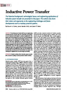
F ar power line
Fig. 1.
weak
Nearby sufficient power line
Depencency of inductive coupling on power lines.
measurement, and wire structures are carefully chosen such that inductive coupling dominates capacitive coupling. The remaining of this paper is organized as follows. Section 2 explains features of inductive coupling effect. Section 3 describes measurement circuit and interconnect structure. Section 4 presents measurement results and discussion. Finally section 5 concludes this paper. II. C HARACTERISTICS OF INDUCTIVE COUPLING NOISE This section briefly describes characteristics unique to inductive coupling; dependency on design parameters, longrange effect and waveform. Inductive coupling effect is intensified/alleviated by power lines, driver sizing, and interconnect width. Figure 1 represents dependency of inductive coupling on power lines. Inductive coupling between two signal lines strongly relies on the overlap of current return paths. When there are power lines wide and close enough, the current loop becomes small and the inductive coupling to other signal lines gets weak. A small driver reduces inductive coupling effect, because a small driver injects less current. In [3], ratio of driver output impedance to characteristic impedance of interconnect is referred as one of the metrics which indicate whether inductive coupling should be considered or not. A narrower interconnect has larger characteristic impedance, and then reduces current injected by the driver, which results in smaller inductive coupling noise. In addition, a narrow interconnect with high resistivity attenuates coupling noise. Figure 2 depicts long-range effect of inductive coupling. Capacitive coupling, which is caused by electric field, is remarkably reduced by distance and signal line insertion. On the other hand, inductive coupling originating from magnetic field is slowly alleviated by distance and signal line insertion. The right graph in Fig. 2 is an example of the coupling coefficient between the leftmost interconnect and no.1-4 interconnect in the bus structure of Fig. 2. The coupling coefficients are normalized by the coefficent of no.1 interconnect. The reduction of the inductive coupling coefficient by the distance is slower than that of the capacitive coupling coefficient, and
24-3-1
721
2
Fig. 2.
3
4
Normalized coupling coef.
1
main path
bypass signal selection
No. of interconnect
bypass circuit
Long-range effect of inductive coupling.
0 1
Fig. 5.
Far-end Voltage (V)
0.1
input signal transition waveform d
0
0
100
200 300 400 Time(ps)
500
output signal transition waveform d/2 d/2
600
An example of coupling noise waveform. Driver
Variable delay
aggressor
Fig. 6.
aggressor
Variable delay
Receiver load
aggressor
Variable delay
victim
Variable delay
aggressor
Variable delay
aggressor
Variable delay
aggressor
Variable delay
aggressor
Variable delay
Phase interpolator.
Receiver
aggressor
Variable delay
bypass
Test pulse input Run/Stop
Pulse output to counter
Fig. 4.
Bypass circuit.
Inductive effect is dominant
-0.05 -0.1
Fig. 3.
Capacitive effect is dominant
0.05
path selector
victim
Measurement circuit structure.
long-range effect of inductive coupling is remarkable. Due to long-range effect, inductive coupling effect increases by superposition of noise waveforms from many aggressors. Figure 3 shows an example of noise waveform considering capacitive and inductive coupling. A sharp spike mainly caused by inductive coupling appears first in Fig. 3, followed by a gentle bump due to capacitive coupling. Inductive effect is observed in much shorter time than capacitive effect, and thus inductive coupling causes delay variation in short timing range. The sharpness makes it difficult to measure inductive coupling noise. III. M EASUREMENT CIRCUIT STRUCTURE A. Measurement circuitry Figure 4 shows the designed circuit to measure interconnect delay variation due to inductive coupling noise. The measurement circuit consists of a victim and eight aggressors in a bus-structure, a ring oscillator, a bypass circuit, a counter, and variable delay circuits. Delay variation of the victim due to coupling noise is measured by the counter as cycle time variation of the ring oscillator. The victim is embedded in the ring oscillator, and rise and fall signals are input to the victim alternately. The observed ring oscillator cycle includes the average of rise and fall signal delays. By using the bypass circuit (Fig. 5), delay
variations for rise and fall transition at victim are separately measured. The bypass circuit generates a bypass delay that is not affected by crosstalk noise. The path selector chooses the main path delay or the bypass delay according to rise/fall transition, and then the only rise or fall delay is captured into the counter and the other is discarded. Relative transition timing between the victim and aggressors is changed with the variable delay circuits. The variable delay circuit consists of a phase interpolator (Fig. 6) [10] and cascaded inverters with selector. The cascaded inverters insert up to the delay of 15 inverters (about 200ps), which is a sufficiently wide timing range for the measurement. The delay variation appears in a short timing range because of sharp spike waveform of inductive coupling noise, and transition timing must be controlled by small time steps. To generate finer aggressor timing than two-stage inverter delay (2tinv ), we introduce a two-stage phase interpolator that divides 2tinv by four. The aggressor timing thus can be controlled by tinv /2. In our implementation, the control and counter signals are stored in scan-chained flip-flops. Therefore this measurement can be easily performed by a pattern generator and a logic analyzer, because all signals are digital and the IO speed of few MHz is fast enough. B. Interconnect structure and TEG variations Figure 7 shows interconnect cross-section of the bus structure, and summarizes basic parameters. Interconnect length and width are decided from practical global interconnects with repeater insertion. We determined the parameters such that inductive coupling dominates capacitive coupling to clearly observe delay variation due to inductive coupling noise; sufficiently large driver size, wide interconnect pitch. Non-thick metal layer (M5) helps to reduce coupling capacitance. Following summarizes variations of TEGs. TEG STD Basic structure TEG with parameters in Fig. 7. TEG M2POWERLINE Parallel power lines with width=2µm and pitch=5µm are located at M2 layer.
24-3-2
722
13 10 µm
V D D & G N D
1µm
aggre s s ors
v i c ti m
aggre s s ors
Orthogonal li ne ( M6 )
12.0
M5
5µm 3 2 X( 4X 1X
V D D & G N D
�
Orthogonal li ne ( M2 -M4)
12 0 Ω) S u b s trate
Fig. 7.
P ow e r li ne ( M1)
measurement RLC SIM RC SIM
10.0
Delay variation(ps)
I nte rc onne c t le ngth I nte rc onne c t w i d th I nte rc onne c t p i tc h D ri v e r s i z e R e c e iv e r R e c e i v e r load
8.0 6.0 4.0 2.0
-100.0
0.0 0.0 -2.0
-50.0
Interconnect cross section.
50.0
100.0
150.0
200.0
-4.0
Aggressor timing(ps)
Fig. 9.
Delay change due to coupling noise on TEG STD.
TEG_STD
Delay variation (ps)
TEG_SMALLDRIVE TEG_NARROWWIRE TEG_M2POWERLINE TEG_LARGELOAD TEG_NODECAP
Fig. 8.
3.5 3.0 2.5 2.0 1.5 1.0 0.5 0.0 0
Micrograph of fabricated chip.
TEG NARROWWIRE Interconnect width is narrowed to 0.14µm. TEG SMALLDRIVE Driver size is decreased to 8X. TEG LARGELOAD Receiver load is increased to 32X. TEG NODECAP Decoupling caps. nearby drivers are removed. TEG STD is designed to measure the delay variation due to inductive coupling clearly. TEG M2POWERLINE, TEG NARROWWIRE, TEG SMALLDRIVE are intended to evaluate the alleviation of inductive coupling effect. TEG LARGELOAD is to evaluate how the receiver loading affects delay change curve. TEG NODECAP aims to reveal whether existence of decoupling capacitance very close to drivers affects inductive coupling noise. A chip in Fig. 8 is fabricated in a 90nm CMOS process with six metal layers and supply voltage is 1.0V. IV. M EASUREMENT RESULT A. Verification of inductive coupling effect Delay variation is computed from measured ring oscillator cycle. Average of five measurements is adopted for the cycle time. Delay variation shown in this paper is average results of three chips. The standard deviation of 200 measurement results is 0.355ps, which demonstrates that our measurement has a good reproductivity to discuss a several ps delay variation. Measurement results are compared with circuit simulation results. Two interconnect models are used: 1) RLC-distributed ladder model (RLC model), and 2) RC-distributed ladder model (RC model). Resistance (R), capacitance (C) and inductance (L) of interconnects are extracted by a 3D field solver [11]. R and L values at 17GHz (significant frequency of driverinput [12]) are adopted for circuit simulation. Figure 9 shows delay variation when all aggressors and victim make rise transition. Relative transition timing between victim and aggressors is changed where all aggressors change simultaneously. There is a remarkable difference between RC
1
2
3
4
5
6
Num. of active aggressors
7
8
Fig. 10. Measurement result of delay change on TEG STD at aggressor timing = 180ps.
and RLC models in range of 20-60ps aggressor timing, which comes from consideration of inductive coupling. The curve of the measurement result follows the simulation result with RLC model, which reveals inductive coupling affects interconnect delay considerably in 90nm technology. This result indicates that RLC-distributed ladder model is effective for noise-aware timing analysis. The difference of delay variation between measurement and RLC simulation result is found in the range of below 0ps and over 60ps aggressor timing. This difference is due to power supply noise by aggressors which is not considered in simulation. Figure 10 indicates that delay increase at aggressor timing = 180ps, where the aggressor and victim transitions are not overlapped, is proportional to number of active aggressors and implies that measurement delay is increased by power supply noise slightly. We next changed the transition direction between the aggressors and the victim, and measured delay change curve. Figure 11 includes two curves; victim rise and aggressor fall, and victim fall and aggressor rise. As the transition timing gets closer, the delay variation decreases, which is different from Fig. 9. This result confirm that the measured delay variation comes from interconnect coupling noise. The bypass circuit in Fig. 5 enables us to measure two delay change curves for rise and fall transitions separately. B. Evaluation of inductive coupling characteristics Figure 12 demonstrates long-range effect of inductive coupling. We measured delay variation caused by four active aggressors varying aggressor positions. As the active aggressors become distant, the delay variation becomes small, but its decreasing speed is slow. Even though two quiet wires exist between the aggressors and victim, the delay variation is only reduced to the half, because inductive coupling is not easily shielded by signal lines and is slowly weakened by distance. Figures 13-16 demonstrate how much noise suppression techniques and design parameters influence delay variation
24-3-3
723
50.0
100.0
150.0
200.0
-100.0
Delay variation(ps) -100.0
4.0 3.0 2.0 1.0 -50.0
0.0 0.0
50.0
100.0
Aggressor timing(ps)
150.0
200.0
Delay variation(ps)
7.0
��������� ��������� ���������
100.0
150.0
200.0
Fig. 13. Measurement of TEG M2POWERLINE. Parallel wires in M2 weakens inductive coupling.
Fig. 11. Measurement result of delay change on TEG STD. Opposite direction transitions are shown.
5.0
50.0
Aggressor Timing(ps)
Aggressor timing (ps)
6.0
TEG_STD TEG_M2POWERLINE
-100.0
Fig. 12. Measurement result of delay change when far aggressors are active.
comparing with TEG STD. (a) Adding parallel ground wires in the lower layer (TEG M2POWERLINE) reduces delay variation by 3ps, because inductive coupling becomes weak. (b) Narrowing signal interconnects (TEG NARROWWIRE) decreases delay variation by 4ps, because higher resistance of narrower wires damps inductive effects. (c) Reducing driver sizes (TEG SMALLDRIVE) decreases delay variation, because a driver with high output impedance injects less voltage and current into interconnects. (d) Enlarging receiver loading (TEG LARGELOAD) increases susceptive timing range, because slower receiver transition makes timing range wider to be attacked by inductive noise. (e) Reducing adjacent decoupling capacitance (TEG NODECAP) does not affect measurement results. The above measurements (a)-(d) agree with qualitative discussion and circuit simulation, which clarifies noise suppression techniques developed based on simulation will be effective. V. C ONCLUSION In summary, we measured a significant effect of inductive coupling on timing in 90nm global interconnects, and revealed inductive coupling has become a practical design issue in advanced technologies. Interconnect models are evaluated, and RLC-distributed ladder model follows measurement results. We also verified characteristics unique to inductive coupling, such as long-range effect and shielding effect by ground wires on silicon. Mitigation effects of inductive coupling with power lines, driver sizing, and narrowed wire are verified from measurement results.
10.0 9.0 8.0 7.0 6.0 5.0 4.0 3.0 2.0 1.0 0.0 -50.0 0.0
Delay variation(ps)
10.0 9.0 8.0 7.0 6.0 5.0 4.0 3.0 2.0 1.0 0.0 -50.0 0.0
-100.0
10.0 9.0 TEG_STD 8.0 TEG_NARROWWIRE 7.0 6.0 5.0 4.0 3.0 2.0 1.0 0.0 -50.0 0.0 50.0 100.0 150.0 200.0 Aggressor timing(ps)
Fig. 14. Measurement of Narrow TEG NARROWWIRE. signal wires damp inductive noise. 14.0
TEG_STD TEG_SMALLDRIVE
50.0
100.0
Aggressor timing(ps)
150.0
200.0
Fig. 15. Measurement of TEG SMALLDRIVE. Small driver injects less noise.
-100.0
TEG_STD TEG_LARGELOAD
12.0
Delay variation(ps)
Vic rise/Agg fall Vic fall/Agg rise
Delay Variation(ps)
Delay variation (ps)
-100.0
9.0 8.0 7.0 6.0 5.0 4.0 3.0 2.0 1.0 0.0 -50.0 0.0 -1.0 -2.0
10.0 8.0 6.0 4.0 2.0 -50.0
0.0 0.0
50.0
100.0
Aggressor timing(ps)
150.0
200.0
Fig. 16. Measurement of TEG LARGELOAD. Large receiver load enlarges noise susceptive timing.
of Tokyo, with the collaboration by STARC, Fujitsu Limited, Matsushita Electric Industrial Company Limited., NEC Electronics Corporation, Renesas Technology Corporation, and Toshiba Corporation. This study was partly supported from NEDO of Japan.
R EFERENCES [1] Y. Massoud, J. Kawa, D. MacMillen, and J. White, “Modeling and analysis of differential signaling for minimizing inductive crosstalk,” in Proc. DAC, pp. 804–809, June 2001. [2] S. Seongkyun, E. Yungseon, W. R. Eisenstadt, and S. Jongin, “Analytical models and algorithms for the efficient signal integrity verification of inductance-effect-prominent multicoupled VLSI circuit interconnects,” IEEE Trans. VLSI Systems, vol. 12, no. 4, pp. 395–407, Apr. 2004. [3] A. Deutsch, et al., “On-chip wiring design challenges for gigahertz operation,” Proc. of the IEEE, vol. 89, no. 4, pp. 529–555, Apr. 2001. [4] S. C. Chan and K. L. Shepard, “Practical considerations in RLCK crosstalk analysis for digital integrated circuits,” in Proc. ICCAD, pp. 598–604, Nov. 2001. [5] A. Muhtaroglu, G. Taylor, T. Rahal-Arabi, and K. Callahan, “On-die droop detector for analog sensing of power supply noise,” in Proc. Symp. on VLSI Circuits, pp. 193–196, June 2003. [6] K. Shimazaki, M. Nagata, T. Okumoto, S. Hirano and H. Tsujikawa, “Dynamic power-supply and well noise measurement and analysis for high frequency body-biased circuits,” in Proc. Symp. on VLSI Circuits, pp. 94–97, June 2004. [7] M. Takamiya and M. Mizuno, “A sampling oscilloscope macro toward feedback physical design methodology,” in Proc. Symp. on VLSI Circuits, pp. 240–243, June 2004. [8] T. Sato, D. Sylvester, Y. Cao, and C. Hu, “Accurate in-situ measurement of noise peak and delay induced by interconnect coupling,” IEEE JSSC, Vol. 36, No. 10, pp. 1587–1591 Oct. 2001. [9] Y. Ogasahara, M. Hashimoto, T. Onoye, “Measurement and analysis of delay variation due to inductive coupling,” in Proc. CICC, pp. 305–308, Sep. 2005. [10] B. W. Garlepp, et al., “A Portable digital DLL for high-speed CMOS interface circuits,” IEEE JSSC, vol. 34, no. 5, May 1999. [11] Synopsys Corp., “Raphael interconnect analysis program reference manual,” June 2004. [12] C. Cheng, J. Lillis, S. Lin, and N. H. Chang, “Interconnect analysis and synthesis,” Wiley-Interscience Publication, 2000.
ACKNOWLEDGMENT The VLSI chip in this study has been fabricated through the chip fabrication program of VLSI Design and Education Center(VDEC), the University
24-3-4
724