The first phase aims to generate an optimal abstract representation of the logic circuit, a ... single output, K-input connected subgraphs (fanout free cones). Fig. 1.
Optimal Implementation of Combinational Logic on Look-up Tables Kubilay Atasu, Tim Todman, Oskar Mencer and Wayne Luk Department of Computing, Imperial College London {kubilay.atasu,tjt97,o.mencer,w.luk}@imperial.ac.uk Abstract— We present a methodology for optimally implementing combinational logic equations on networks of look-up tables. Our work effectively extends optimality to span logic minimization and technology mapping. We restrict ourselves to 4-input look-up tables (LUTs) and enumerate all possible circuits up to a certain area or latency. Since simple-minded enumeration would take a long time, we develop levels of abstractions (steps) and we formulate the key step of enumeration as an Integer Linear Programming (ILP) problem. We show results on a set of ISCAS benchmarks.
I. I NTRODUCTION We address the problem of optimization of designs for reconfigurable hardware. We use enumeration to optimize logic. In principle, we enumerate every possible configuration of a device. In practice, we simplify the enumeration to only consider configurations and connections of look-up tables (LUTs) on Field-Programmable Gate Array devices (FPGAs), under area and latency constraints. For this paper, we only consider combinatorial designs, including the state-transition logic of finite state machines. The traditional approach in logic synthesis for FPGAs is based on two phases: technology independent optimization, and technology mapping [5]. The first phase aims to generate an optimal abstract representation of the logic circuit, a Boolean network most of the time. The second phase tries to transform the abstract representation into a network of primitive logic functions implemented by the available library, in our case 4-input look-up tables. Although two level logic minimization can be done very efficiently [6], finding the optimum factored form of a logic function is a very complex problem, and existing methods for the first phase are heuristic or approximate. A large body of research efforts has concentrated on the technology mapping problem for LUT-based FPGAs in the last decade. An algorithm to find delay-optimal mappings was described in [10]. On the other hand, it has been proven that the problem of finding area-optimal mappings for LUTs of input size four and greater is an NP-hard problem [7]. The early work on area minimization relied on decomposition of the circuit into a set of trees, and applied technology mapping on tree structures [8], [9]. Although area minimization on trees is much easily solvable, real circuits are rarely trees and this approach misses optimal solutions across tree boundaries. Cong et al. concentrated on enumeration of single output, K-input connected subgraphs (fanout free cones)
Fig. 1. Our approach to enumeration. Step 2 differs for area (step 2a) and latency (step 2b). In Steps 3 and 4, we use an ILP approach.
within the circuit, and proved that the problem can still be optimally solved by decomposing the circuit into maximal fanout free cones (MFFC), and enumerating separately on each MFFC in [11]. The proposed algorithm although very practical, had exponential worst case complexity, and restricted the solution to duplication free mappings where each circuit gate must be mapped to exactly one LUT. Later work by Cong et al. [12] introduced heuristics to reduce the runtime, and extended the approach to duplicable mappings. More recent work, reformulating the technology mapping problem as a boolean satisfiability problem, has shown that state-of-the-art FPGA technology mapping algorithms miss optimal solutions [13]. Enumeration guarantees that all solutions are considered; one can obtain the absolute lower bound of logic resources needed to implement a particular problem. Little related work has been reported on using enumeration for design optimization. A recent effort concerns an implicit technique for enumerating structural choices in circuit optimization based on re-wiring and re-substitution [14]. In [15],
Shape
LUT
Internal connection possibilities
(1) LUT
(1,1)
n LUT LUT
1
(1,1,1)
LUT
n
1
LUT
(2,1)
(a) One Layer
Fig. 2.
(a) Two Layers
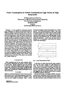
Examples of designs with one and two layers of LUTs.
a reconfigurable hardware implementation is proposed to accelerate circuit enumeration. Our research differs from [14], [15], since we use an ILP-based approach to implement the key step of enumeration. Our three main contributions in this paper are: • Extending optimality to span logic minimization and technology mapping. • A 4-step process to enumerate all possible solutions. • Implementation via software enumeration, and Integer Linear Programming. Our overall approach to enumeration is illustrated in Figure 1, showing how we break the problem into several steps: Step 1 Given a boolean input function and an optimization metric (area or latency), this step identifies observable inputs and limits the search space. Step 2 Enumerate all circuit shapes within the search space from step 1, sort by (a) latency or (b) area, Step 3 Enumerate all possible interconnections for each shape, Step 4 Enumerate all possible LUT configurations for each circuit. II. T HEORY In this section we develop expressions for the upper bound of the design space for enumeration, for each step of Figure 1. We assume layers of LUTs (shapes) to realize a design, and we enumerate different LUT configurations and interconnections. Some possible shapes and internal connections for enumerating a design is shown in Figure 3. We assume that the truth table for an N-bit input, 1-bit output function Y is given as in Table I. We assume that the function has already been reduced so all of the inputs are observable. Observability of an input can be computed using Boolean derivative as defined in [4]. We enumerate designs consisting of 4-bit LUTs (A 4-bit LUT has 4 inputs). We assume that the circuit is composed of H layers of LUTs, where layer h is composed of Lh LUTs. We define Ltot as the total number of LUTs contained in the design. The design space for enumeration is large: a 4-bit LUT can 4 be configured in 22 ways. A logic function with 4 inputs can
(2,1,1)
Fig. 3. Some internal connection possibilities for several shapes. Vertical lines separate the layers. (Step 3) 0 0 .. . c0,t .. . 1
1 0 .. . c1,t .. . 1
... 0 .. . ... .. . 1
i 0 .. . ci,t .. . 1
... 0 .. . ... .. . 1
N-1 0 .. . cN−1,t .. . 1
Y y0 .. . yt .. . y2N −1
TABLE I T RUTH TABLE FOR AN N- BIT INPUT 1- BIT OUTPUT FUNCTION
be implemented with a single LUT. Logic functions with larger number of inputs require multiple LUTs. We further refine different steps of Figure 1 to handle N-input logic functions: Step 1 We identify observable inputs and index into Table II to find the range of our design space with associated area and latency requirements. The maximum latency and area requirements are calculated based on the following observations: • a 4-input design can be implemented by a single LUT, • an n + 1-input design can be implemented using two n-input designs, and an additional LUT multiplexing between the two using the n + 1th input. The minimum area and latency requirements are calculated based on the following observations: • each observable design input must be connected to at least one LUT input, • at least one of the LUT inputs must be connected to a LUT output at a previous layer, • there is a single LUT at the highest layer. Step 2 We find all shapes for the range found in step 1 (See Table III). We sort the resulting list of shapes by latency (if optimizing for latency, step 2a) or area (if optimizing for area, step 2b). For example, to enumerate an 8-input design for minimum area, we first choose the smallest topology that will accept eight inputs: (2,1) in our terminology. If this fails, we
function #inputs ≤4 5 6 7 8 9 10 11 N
optimize for latency min max 1 1 2 2 2 3 2 4 2 5 2 6 2 7 2 8 log4 (N) (N − 3) O(logN) O(N)
optimize for area min max 1 1 2 3 2 7 2 15 3 31 3 63 3 127 4 255 ⌊(N + 1)/3⌋ 2N−3 − 1 O(N) O(2N )
TABLE II L ATENCY ( MAXIMUM NUMBER OF LUT S FROM INPUTS TO OUTPUT ) AND AREA ( NUMBER OF LUT S ) FOR DIFFERING NUMBERS OF INPUTS . U SER INPUT TO OPTIMIZATION IS
# INPUTS AND OPTIMIZATION MODE
( LATENCY OR AREA ). (S TEP 1)
Latency 1 Area 1 2 3 4 5 6
2
3
4
5
(1) (1,1) (2,1) (3,1) (4,1)
(1,1,1) (2,1,1) (1,2,1) (3,1,1) (1,3,1) (2,2,1) (4,1,1) (3,2,1) (2,3,1) (1,4,1)
(1,1,1,1) (2,1,1,1) (1,2,1,1) (1,1,2,1) (3,1,1,1) (2,2,1,1) (1,3,1,1) (2,1,2,1) (1,2,2,1) (1,1,3,1)
This section has shown the size of the search space for enumeration. The next section introduces our ILP formulation to solve the LUT mapping problem exactly. III. E NUMERATION U SING ILP We describe an Integer Linear Programming formulation to achieve Steps 3 and 4 together. The ILP formulation checks if there exists a feasible circuit given a shape from Step 2. We define a binary decision variable Xh,l,k,i which represents whether input i is connected to the kth input of the lth LUT at layer h. More formally: 1 if input i is connected to the kth input Xh,l,k,i = of the lth LUT at layer h 0 otherwise h ∈ {0..H − 1} , l ∈ {0..Lh − 1}, k ∈ {0..3} , i ∈ {0..N − 1} (1) We define a binary decision variable XOUTh,l,k,hi,li which represents whether output of the lith LUT at layer hi is connected to the kth input of the lth LUT at layer h: XOUTh,l,k,hi,li ∈ {0, 1} , hi ∈ {0..h − 1}, li ∈ {0..Lhi − 1}
(1,1,1,1,1) (2,1,1,1,1) (1,2,1,1,1) (1,1,2,1,1) (1,1,1,2,1)
TABLE III A LL THE DIFFERENT SHAPES FOR ONE TO FOUR 4-LUT S , ARRANGED ACCORDING TO LATENCY AND AREA . (S TEP 2)
(2) We associate a binary decision variable with each configuration bit of each LUT. For LUT l of layer h, we need to define 2K new decision variables: � LUTh,l, j ∈ {0, 1} , j ∈ 0..2K − 1 (3) We associate a binary decision variable with each LUT output. The output of LUT l of layer h at time t is represented as OUTh,l,t : � OUTh,l,t ∈ {0, 1} ,t ∈ 0..2N − 1 (4) Each LUT input must be connected to exactly one function input or one LUT output at a lower layer:
choose one of the next smallest designs, and so on. Similarly, the minimum latency design can be found by iterating from the minimum latency topology to the maximum. Step 3 We enumerate all interconnection possibilities. One of the LUT inputs must be connected to a LUT output at a previous layer. The remaining inputs may connect to the output of any LUT in a previous layer, or to a design input. Step 4 For all graphs, we enumerate each configuration of 4 each LUT. For Ltot LUTs, this is 22 ∗Ltot . The output of the final circuit must be identical to the N-bit function output specified by a truth table for each input over the input space of 2N (See Table I). To make enumeration more tractable, we only consider combinatorial designs (no registers or feedback) with single output. Enumeration can still be applied to the combinatorial parts of sequential designs. Multiple-output designs can still be considered by generating separate hardware for each output, followed by a common-subexpression elimination step to eliminate LUT configurations and connections common to several outputs.
∑i∈{0..N−1} (Xh,l,k,i ) + ∑hi∈{0..h−1} ∑li∈{0..Lhi −1} (XOUTh,l,k,hi,li ) = 1
(5)
We define a new binary decision variable Zh,l,k,t which stores the value assigned to the kth input of the lth LUT at layer h at time t: Zh,l,k,t =
∑
(Xh,l,k,i ∧ ci,t ) +
i∈{0..N−1}
∑
∑
hi∈{0..h−1} li∈{0..Lhi −1}
(XOUTh,l,k,hi,li ∧ OUThi,li,t )
(6) We calculate the output of the lth LUT at layer h at time t as follows: (Zh,l,0,t ∧ Zh,l,1,t ∧ Zh,l,2,t ∧ Zh,l,3,t ∧ LUTh,l,0 )∨ (Zh,l,0,t ∧ Zh,l,1,t ∧ Zh,l,2,t ∧ Zh,l,3,t ∧ LUTh,l,1 )∨ . OUTh,l,t = .. (Zh,l,0,t ∧ Zh,l,1,t ∧ Zh,l,2,t ∧ Zh,l,3,t ∧ LUTh,l,2K −2 )∨ (Zh,l,0,t ∧ Zh,l,1,t ∧ Zh,l,2,t ∧ Zh,l,3,t ∧ LUTh,l,2K −1 ) (7)
The output of the highest layer LUT must be identical to the N-bit function output for the same set of inputs. The optimal solution returns an objective value equal to zero if and only if a circuit implementing the given functionality is found: min
∑
|yt − OUTH−1,0,t |
(8)
Name c17
#Inps 5
s27
7
b01
7
b02
5
t∈{0..2K −1}
IV. R ESULTS
AND EVALUATION
Our tool chain starts with the truth table specification of a given logic function. We traverse Table III columnwise or rowwise depending on the optimization mode (latency or area respectively). For each shape we automatically generate the associated ILP problem, and solve using CPLEX Mixed Integer Optimizer [16]. The process is continued until a feasible circuit implementing the given function is found. Once a circuit is found, we automatically generate the hardware description in ASC [17], explicitly specifying the LUT configurations and interconnections to be mapped onto an actual FPGA. Additionally, for each circuit, we automatically generate a testbench, and simulate for the set of inputs specified in the truth table, comparing the result with the expected output. In this way we verify the correctness of the circuits we generate. We have applied our algorithms on a set of ISCAS benchmarks shown in Table IV. The benchmarks describe circuits with multiple inputs and outputs. Most of the time an output is sensitive to changes in a subset of the inputs only (i.e., observable inputs). Therefore only a subset of the circuit inputs have to be considered during enumeration. The shapes automatically identified for the benchmarks, together with the execution time of the ILP solver are given in in the last two columns of Table IV. In all cases, where ILP completed successfully, only two LUTs (i.e., a shape of (1,1)) were sufficient to realize the output functions. We have observed that the number of constraints increased quickly with the number of inputs, and ILP did not complete within 24 hours in two of the cases. V. C ONCLUSION We have described an enumeration approach for identifying optimal combinational circuit implementations on networks of look-up tables. We divide the enumeration into steps that enable efficient exploration of the search space. We explore different circuit topologies (shapes) in the order of latency or area, depending on the optimisation mode. We make use of the existing ILP technology [16] to carry out the key step of enumeration, where we identify whether a chosen shape is feasible for implementing a given logic function. Our current and future work involves improving the speed of enumeration for the optimization of larger logic functions. In particular, we are exploring more efficient ILP formulations that can better exploit symmetries within a circuit. Additionally, we are planning to evaluate the performance of hybrid techniques that combine software enumeration, hardware enumeration [15], and ILP.
Output 1 2 1 2 3 4 1 2 3 4 5 6 7 1 2 3 4 5
#Obs.Inps 4 4 6 5 6 3 1 1 3 5 5 5 5 2 3 4 4 4
Shape (1,1) (1,1) (1,1) (1,1) (1,1) (1,1) (1,1) (1,1) (1,1) (1,1) (1,1) (1,1) (1,1) (1,1) (1,1) (1,1)
Run-time 0s 0s 42 s 0s 0s 0s 0s 17397 s 972 s 1120 s 156 s 0s 0s 0s 0s 0s
TABLE IV R ESULTS FOR A SET OF ISCAS BENCHMARKS . RUN - TIMES ARE GIVEN IN SECONDS . ILP DID NOT COMPLETE IN TWO OF THE CASES .
R EFERENCES [1] D. E. Knuth, “A Draft of Section 7.2.1.3: Generating All Combinations”, The Art of Computer Programming: Pre-Fascicle 3A, 2005 [2] R. L. Graham, D. E. Knuth, O. Patashnik, Concrete Mathematics: A Foundation for Computer Science, Addison-Wesley, 1989. [3] S. J. Russell and P. Norvig, Artificial Intelligence: A Modern Approach, Prentice Hall, 1995. [4] G. De Micheli, Synthesis and Optimisation of Digital Circuits, McGrawHill, 1994. [5] A. Sangiovanni-Vincentelli, A. El Gamal, and J. Rose. “Synthesis methods for field programmable gate arrays”. Proceedings of IEEE, pp. 1057–1083, July 1993. [6] R. K. Brayton, C. McMullen, G. D. Hachtel, and A. SangiovanniVincentelli. “Logic Minimization Algorithms for VLSI Synthesis”. Kluwer Academic Publishers, 1984. [7] A. Farrahi, and M. Sarrafzadeh. “Complexity of the Lookup-Table Minimization Problem for FPGA Technology Mapping”. IEEE Transactions on Computer-Aided Design of Integrated Circuits and Systems, 13(11):1319–1332, 1994. [8] K. Keutzer. “DAGON: Technology Binding and Local Optimization by DAG Matching”. In DAC 1987, pp. 341–347. [9] R. Francis, J. Rose, and Z. Vranesic. “Chortle-crf: Fast Technology Mapping for Lookup Table-Based FPGAs”. In DAC 1991, pp. 227–233. [10] J. Cong and Y. Ding. “An Optimal Technology Mapping Algorithm for Delay optimization in Lookup-Table Based FPGA Designs”. In IEEE ICCAD, 1992. [11] J. Cong, and Y. Ding. “On area/depth trade-off in LUT-based FPGA technology mapping”. In DAC 1993, pp. 213–218. [12] J. Cong, C. Wu, and Y. Ding. “Cut ranking and pruning: enabling a general and efficient FPGA mapping solution”. In FPGA 1999, pp. 29– 35. [13] A. Ling, D. P. Singh and S. P. Brown, “FPGA Technology Mapping: A Study of Optimality”, In DAC 2005. [14] V. N. Kravets and P. Kudva, “Implicit Enumeration of Structural Changes in Circuit Optimization”, In DAC 2004, pp. 438–441. [15] T. Todman, H. Fu, O. Mencer, and W. Luk. “Improving Bounds for FPGA Logic Minimization”. In FPT 2007, pp. 245–248. [16] ILOG CPLEX. http://www.ilog.com/products/cplex/ [17] O. Mencer, “ASC, A Stream Compiler for Computing with FPGAs” IEEE Transactions on CAD, IEEE, 2006.