Prototype Readout Module for the ATLAS Level-1 Calorimeter Trigger Processors G. Anagnostou, P. Bright-Thomas, J. Garvey, S. Hillier, G. Mahout, R. Staley, W. Stokes, S. Talbot, P. Watkins, A. Watson School of Physics and Astronomy, University of Birmingham, Birmingham B15 2TT, UK
R. Achenbach, P. Hanke, W. Hinderer, D. Kaiser, E.-E. Kluge, K. Meier, U. Pfeiffer, K. Schmitt, C. Schumacher, B. Stelzer Kirchhoff Institut für Physik, University of Heidelberg, D-69120 Heidelberg, Germany
B. Bauss, K. Jakobs, C. Nöding, U. Schäfer, J. Thomas Institut für Physik, Universität Mainz, D-55099 Mainz, Germany
E. Eisenhandler, M.P.J. Landon, D. Mills, E. Moyse Physics Department, Queen Mary, University of London, London E1 4NS, UK
P. Apostologlou, B.M. Barnett, I.P. Brawn, J. Edwards, C.N.P. Gee, A.R. Gillman,R. Hatley, V. Perera, A.A. Shah, T.P. Shah Rutherford Appleton Laboratory, Chilton, Didcot OX11 0QX, UK
C. Bohm, S. Hellman, S.B. Silverstein Fysikum, University of Stockholm, SE-106 91 Stockholm, Sweden
Corresponding author: Gilles Mahout (
[email protected]) Abstract The level-1 calorimeter trigger consists of three subsystems, namely the Preprocessor, electron/photon and tau/hadron Cluster Processor (CP), and Jet/Energy-sum Processor (JEP). The CP and JEP will receive digitised calorimeter trigger-tower data from the Preprocessor and will provide trigger multiplicity information to the Central Trigger Processor and region-of-interest (RoI) information for the level-2 trigger. It will also provide intermediate results to the data acquisition (DAQ) system for monitoring and diagnostic purposes. This paper will outline a readout system based on FPGA technology, providing a common solution for both DAQ readout and RoI readout for the CP and the JEP. Results of building a prototype readout driver (ROD) module will be presented, together with results of tests on its integration with level-2 and DAQ modules.
I. INTRODUCTION The ATLAS Level-1 Calorimeter Trigger is described in [1]. It consists of three subsystems: the Preprocessor (see accompanying paper on MCM), the electron/photon and
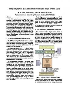
tau/hadron Cluster Processor (CP), and Jet/Energy-sum Processor (JEP). The CP and JEP will receive digitised calorimeter trigger-tower data from the Preprocessor, and will provide multiplicity information on trigger objects to the Central Trigger Processor via Common Merger Modules (CMMs). For a more detailed overview of the trigger, see the accompanying talk on “One Size Fits All”. Using Readout Driver (ROD) modules (fig. 1), the CP and JEP must also provide region-of-interest (RoI) information for the level-2 trigger, and readout data to the data acquisition (DAQ) system for monitoring and diagnostic purposes. The ROD modules used for the Cluster Processor and the Jet/Energy-sum Processor are based on FPGA technology. We will use one common design for both subsystems, using appropriate firmware to handle the several different types of RoI and trigger readout data. In order to see if such a design is feasible, a prototype ROD module has been built. We will first summarise the requirements and functionality of this prototype. The readout process and hardware implementation are then described, followed by first test results from both standalone tests and integration with ATLAS level-2 trigger and DAQ modules.
Cluster Processor Jet/Energy Jet Energy Processor x4 ◊4 C C C M P P M MM
14
C T MC MM
x2 ◊2 J J J C ME E M MM
16
CT S MC MM
G-link T T C v x
TR RRR R TOOOO O CDDDD D v i
◊2 x2
S-link DAQ
Level-2
Figure 1: Readout path of the Cluster and Jet/Energy Processors.
II. TRIGGER REQUIREMENTS The CP and JEP find trigger objects of various types for each bunch crossing, and send the multiplicity for each type to the Central Trigger Processor. The CP identifies isolated electron/photon showers (between 8 and 16 sets of thresholds in E T ) and isolated single-hadron/tau candidates (up to 8 threshold sets in ET for a grand total of 16 threshold sets). The JEP identifies jets above 8 ET thresholds, as well as triggering on missing-ET, total-ET, forward jets, and total jet ET. Coordinates of all the objects found, as well as the total value and components of ET , must be sent to the level-2 trigger as RoI information for all bunch crossings which generate a level-1 trigger in the CTP.
III. READOUT DRIVER REQUIREMENTS The Readout Driver module collects data from CP Modules (CPMs and CMMs) and JEP Modules (JEMs and CMMs). It formats the data and sends it on to the DAQ and to level-2 (RoIs). The ROD requirements are as follows: • Collect data from several trigger processing modules • Read out data from more than one consecutive bunchcrossing (‘slice’) if required • Perform error detection on received data • Process data, including zero suppression when needed • Format DAQ and RoI data • Interface to the readout S-link [2] • Monitor the data sent on the S-link via a spy • Receive TTC signals and commands [3] • Interface to CTP (ROD busy signal) • Operate at level-1 event rate of up to 100 kHz
IV. READOUT PROCESS Readout data for monitoring trigger operation and performance comprise the input data and results of the CPMs, JEMs and CMMs. RoI data for discrete trigger objects comes from the CPMs and JEMs, and energy-sum results from CMMs in the JEP. Because level-1 triggers are asynchronous, we have chosen to use 20-bit G-links [4] to transmit the data to the RODs, with two links per trigger module — one for DAQ data and one for RoIs. The RODs receive and buffer the serialised 20-bit data using a G-link receiver mezzanine board On receipt of the level-1 accept signal (L1A), the ROD’S control logic places the event number and the bunch-crossing number (BCID) generated by the TTC [3] into the event and the BCID buffer. It also checks how many ‘slices’ (1–5) of trigger-tower data to read out. When the ROD receives the Glink Data AVailable (DAV) signal, the controller takes the event number and the BCID number from these buffers and places them in the header buffer FIFO and then initiates the zero-suppression logic. The control logic also checks the received BCID number against the TTC-generated number and flags an error if they are not in agreement. The controller also monitors the Xoff signal from the DAQ Readout Subsystem (ROS) to stop any data transfer in case it is getting full. Since the Xoff prevents the data transfer out of the ROD module, the incoming data may fill the ROD buffers. In this situation, before the ROD buffers are completely full the ROD must indicate to the Central Trigger Processor via the BUSY signal to stop sending data. The principle of data transfer for the RoIs is the same except for the bit-field definitions, and the additional requirement for terminating RoI transmission to level-2 if there are too many RoIs in the event.
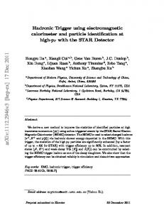
V. IMPLEMENTATION OF THE PROTOTYPE A ROD prototype has been built in order to demonstrate the data transfer from multiple data sources to a data sink. The prototype has four input channels, whereas the final ROD will probably have 18 channels. Fig. 2 shows its block diagram and fig. 3 a photograph. Its functionality is as follows: • Input on 800 Mbit/s G-link Rx daughter cards • Compare transmitted bunch-crossing numbers with onboard TTCrx-generated numbers, and set error flag in readout data if they do not match • Perform parity check on the incoming data • Perform zero suppression on trigger-tower data for each channel, if needed • Write formatted data to FIFO buffers • Transmit data to the RoIB and the DAQ Readout Subsystem using S-link • Provide an event buffer, accessible via VME, to spy on the S-link data • Provide a PCI interface for processing the spy-buffer data using an FPGA or PCI DCP mezzanine card
The implementation has the following features: • Triple-width 6U VME module • Four Common Mezzanine Card positions: o One G-link (HDMP-1024) 4-channel daughter card o Two S-link daughter cards o One position for a commercial PMC co-processor card • All processing and data-handling carried out by FPGAs
transmitters and receivers to be used. FPGAs on the DSS can be used to generate pseudo-random data for transmission, and the data received can be compared automatically with what was transmitted in order to search for errors at very high speeds, thus permitting detection of bit errors with very high sensitivity. Data memories on the DSS are also accessible via VME for various other types of monitoring.
• The same module with different firmware will handle CPMs, JEMs or CMMs, and DAQ and/or RoI data • Off-the-shelf S-link card to transfer data out • Spy on events for monitoring using 32 kbyte buffer • TTCdec decoder card [5] to interface to TTC system Note that for testing purposes the ROD can send duplicate copies of the same fragments in parallel over both S-links. Header
Receiver CMC Shift register output from the FIFO
D0 CH 1
G-Link Rx
Parity Check & Zero Suppression Logic
DATA FPGA
D19
Sub-header
Data
Data
Wr-En Rd-En[0]
Shift register output from the FIFO
Data Buffer
DAV
Shift register output from the FIFO
D0
CH 4
G-Link Rx
DATA FPGA
D19
Parity Check & Zero Suppression Logic
Data
Sub-header
Wr-En Rd-En[3]
Data Buffer
Shift register output from the FIFO
Status Register DAV Rd-En [0:3]
Status Count
XOFF Data Count
DAV 1-4
Trailer
En-Zero suppression
LHC clock L1A
32
BCnt[11:0]
Controller FPGA
start and end marker
BCntRes
S-Link (CMC) (1)
Dout [7:0]
DAQ
BCntStr
Figure 3: The 6U prototype ROD module.
TCM DQ[3:0] TTCrx start and end marker
TTC
TTC Module
TTC Module
S-Link (CMC) (2)
[7:0]
RoI
DoutStr SubAddr
TTC
Brcst[7:2] Interrupt to the SBC BrcstStr1 ROD Busy
Spy Event Buffer (Selected Sample for Local Monitoring) ROD Busy
DSS Module
VME registers
Trigger Type
To Header + controller
FPGA(DSP)
ROD Module
G-Link Tx G-Link Rx (Emulate CPM)
FIFO S-Link interface
BCID Number n
PCI interface Spy buffer manager
BCID Number 1
Interface to Single BCID FIFO
To Header + controller
Board Computer (SBC)
To the SBC via VME
VME Interface
BrcstStr2
(Emulate ROB)
S-Link (S)
XOFF
Figure 4: The standalone test setup.
Event Number n Event Number 1
Data Data/Control Signal
S-Link (D)
PCI Interface
A. Standalone test
For the ROD prototype test, a 4-channel G-link transmitter card emulated the readout logic for DAQ and RoI data on the CPMs to feed input data to the ROD, and an S-link receiver card was used as the destination for output data transmitted by the ROD. This arrangement is shown in fig. 4.
A Data Source/Sink module (DSS) [5] has been designed and built, to allow a variety of tests on different modules. The use of daughter cards allows several different types of data
The DSS firmware was configured to generate a packet of serial data on the G-links following each level-1 accept received from the TTC. The packet content was obtained from
Figure 2: Block diagram of prototype ROD module.
VI. TEST RESULTS
an internal DSS memory which was pre-loaded with data corresponding to a range of RoI content at different stages during the tests. Data arriving over the S-link was captured in a 32 kbyte memory and could later be read from VME. For much of the testing a sequence of closely spaced L1A signals was generated by a burst-mode pulse generator and distributed by the TTC system. On each L1A, RoI data were generated and transmitted by the DSS, received and reformatted by the ROD, transmitted over S-link, received by the second DSS daughter card, and captured in DSS memory. The number of L1As per burst was chosen so that all S-link RoI packets generated in one burst by the ROD could be recorded in the DSS memory without overwriting. For each burst, the recorded S-link data were read out by the online computer and compared with what was expected. All events in the burst were different, with a cyclical pattern used to check correct ROD processing of a variety of RoI data. The test program could not check the bunch-crossing number copied into each event from the TTC by the ROD, but it did check that the event number increased monotonically through the run. It was found that this test could routinely be run overnight without any errors at L1A burst frequencies beyond 800 kHz, exceeding the required 100 kHz by a large factor. It should be noted that the DSS could sustain incoming S-link data at the full speed of the S-link, so did not normally use the S-link’s flow control features.
B. Integration tests The primary purpose of the tests was to check that data could be transferred completely and correctly from the ROD to both the level-2 RoI Builder (RoIB) [6] module and the DAQ Readout Subsystem (ROS). 1) Test setup A diagram of the integration test setup is shown in fig. 5. At different times, both the RoIB and the ROS received the data from the ROD prototype. The RoIB consisted of an input card and the main RoIB card. The input card received S-link data from the ROD, and then prepared and sent two identical copies to the RoIB card, which required at least two input fragments to assemble composite RoI S-link output packets. The ROS consisted of the interface layer to the complete ROS subsystem, running on a conventional Pentium-based PC.
TTC DSS
ROD
Glink Tx CMC
GlinkRx CMC Slink Tx CMC
Slink Rx CMC
PC ROS ROS Slink/PC Slink I Rx CMC
RoIB: Input Input B d
RoI Boar Board B d
Slink Rx CMC
Slink Tx CMC
Figure 5: Schematic view of the integrated test installation.
Testing then continued at lower frequencies, where the protocol errors did not appear. An overnight run with 124byte events containing 16 RoIs was successfully completed without error. The events were generated in bursts of 1024, 2 ms apart in a 3 s cycle, which averaged 418 Hz. In total, 2.1×10⁷ events, corresponding to 2.1×1010 bits, were sent and received without error. The 1024 events in each burst were all different in their RoI content. No events were lost and none was duplicated. 3) ROD BUSY performance Data entering the ROD from the four serial G-links were processed and placed into four FIFOs to await readout. A BUSY threshold inside the ROD was constantly compared with the occupied depth of each FIFO, leading to assertion of the front-panel BUSY signal whenever one or more of the FIFOs was filled up to or beyond the threshold level. The normal operation of the BUSY signal provided a useful tool to monitor the ROD performance.
Three different physical implementations of the S-link were available for use in the tests. All tests with the RoIB used an electrical cable link developed at Argonne National Laboratory (ANL). The links from ROD to DSS were the CERN electrical S-link, and the link to the ROS used the ODIN optical S-link [2]. 2) Results of low-rate tests with RoI Builder For tests with the RoIB, events were transferred in bursts, and the L1A frequency gradually raised until errors occurred, which on investigation proved to be related to incomplete implementation of the S-link flow control protocol.
Figure 6: Timing relationship between L1A (upper trace) and BUSY signal (lower trace), for 16 RoIs. The busy threshold is set at 3.
Fig. 6 shows the behaviour of the BUSY signal when the threshold was set to the artificially low value of 3. This threshold was reached as soon as 3 RoIs had entered the
FIFOs, and remained asserted until the depth of the last FIFO to be emptied fell below 3 again. For events with 16 RoIs, the theoretical minimum busy time (to transfer 13 RoIs over the S-link) is 325 ns. This is in good agreement with the measured time of approximately 400 ns.
completely before triggering the next event burst. This constraint had not been fully appreciated before the test, and has implications for future development of the DSS firmware and other supporting test hardware. 6) Combined tests with the RoIB and ROS
4) Latency measurements The latency of the system was measured using the above configuration and monitoring various test points using a digital oscilloscope. The test points included the L1A, DAV, ROD BUSY and S-link control bit (LFF). The readout sequence is illustrated in fig. 7, for events with 8 RoIs. Transmission on the S-link started 2100 ns after the original L1A. The complete sequence of timing is shown in fig. 8. The total time to the input of the RoIB is less than 3 µs. The ROD itself has a latency of less than 1 µs.
LVL1A
S-link
The prototype ROD is one of the first ATLAS trigger modules to show the feasibility of flexible design using FPGA technology. Firmware can be dedicated to either DAQ or RoI readout. Test results have shown that data could be passed at rates higher that the required level-1 rate with no errors detected over long runs. No hardware design fault was found and the problems occurred in the firmware, which can be easily corrected.
Busy
Figure 7: Readout latency in the DSS/ROD system for 8 RoIs. L1A from TTC
Running with bursts of 127 different events spaced 1 ms apart, several runs of about 2M events were performed, after which the first data error typically appeared. The same errors were detected by software in the RoIB and ROS. Investigation revealed a firmware problem related to the emptying of the ROD FIFOs. This was understood, but it was not possible to obtain a new firmware version before the end of the tests. This test nevertheless established that the ROD could transfer Slink data concurrently to two downstream modules.
VII. CONCLUSIONS
LFF
L1A to TTC
A series of short tests were made with data transmitted over S-link both to the RoIB and to the ROS. This represented exactly the connectivity to be used in the production trigger, where the RoI fragments will be sent both to the RoIB and to the main DAQ readout system.
DAV
BOF
LFF on
LFF off
TTC DSS G-Link
The integration test with downstream modules was essential to the understanding of the interfaces between level1 and the level-2 and dataflow (ROS) systems. Tests were not complete and further work still needs to be done, but good experience has been gained and first results are very encouraging.
CPROD S-Link 150
450
>4 x 25 = 100
550
950
22 x 25 = 550
525 23 x 25 = 525
RoIB 1750 >23 x 66.6 = 1533
ns Measured Expected
REFERENCES
2625
Figure 8: Overall timing from L1A to end of RoIB input card readout.
5) Tests with the Readout Subsystem For testing with the ROS, the S-link interfaces used the ODIN optical S-link. It was found that event frequencies of up to 20 kHz could be sustained into the ROS with full event checking, and that instantaneous L1A frequencies of up to 660 kHz could be sustained, in bursts of 127 events. Very careful control of the ROD was necessary. The DSS module needed to be reset after each burst of events, and the checking software required an exact repeating sequence of 127 events. It was therefore not possible to use the BUSY signal to suppress L1As if the ROD memories became full, so it was essential to wait for the ROD FIFOs to empty
[1] ATLAS First-Level Trigger Technical Design Report, CERN/LHCC/98-14 and ATLAS TDR-12, 30 June 1998: http://atlasinfo.cern.ch/Atlas/GROUPS/DAQTRIG/TDR/t dr.html [2] CERN S-link Specification: http://www.cern.ch/HIS/s-link [3] Timing, trigger and control system (TTC): http://www.cern.ch/TTC/inro.html [4] Agilent G-link information: http://www.semiconductor.agilent.com:80/cgibin/morpheus/home/home.jsp [5] Calorimeter trigger modules: http://hepwww.rl.ac.uk/atlas-l1/Modules/Modules.html [6] R.E. Blair et al., A Prototype RoI Builder for the Second Level Trigger of ATLAS Implemented in FPGAs, ATLAS note ATL-DAQ-99-016, December 1999.