This tutorial makes use of the VHDL design entry method, in which the ... The
screen captures in the tutorial were obtained using the Quartus II version 5.1; ...
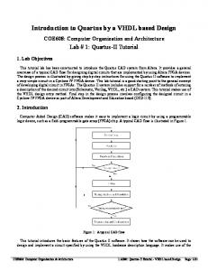
Quartus II Introduction for VHDL Users R This tutorial presents an introduction to the Quartus II software. It gives a general overview of a typical CAD flow for designing circuits that are implemented by using FPGA devices, and shows how this flow is realized in the Quartus II software. The design process is illustrated by giving step-by-step instructions for using the Quartus R II software to implement a simple circuit in an Altera FPGA device. The Quartus II system includes full support for all of the popular methods of entering a description of the desired circuit into a CAD system. This tutorial makes use of the VHDL design entry method, in which the user specifies the desired circuit in the VHDL hardware description language. Another version of this tutorial is available that uses Verilog hardware description language. The screen captures in the tutorial were obtained using the Quartus II version 5.1; if other versions of the software are used, some of the images may be slightly different.
Contents: Typical CAD flow Getting Started Starting a New Project Design Entry Using VHDL Code Compiling the VHDL Code Using the RTL Viewer Specifying Timing Contraints Quartus II Windows
Computer Aided Design (CAD) software makes it easy to implement a desired logic circuit by using a programmable logic device, such as a field-programmable gate array (FPGA) chip. A typical FPGA CAD flow is illustrated in Figure 1.
Design Entry
Synthesis
Functional Simulation
No
Design correct? Yes
Fitting
Timing Analysis and Simulation
No
Timing requirements met? Yes Programming and Configuration
Figure 1: Typical CAD flow. It involves the following basic steps: • Design Entry – the desired circuit is specified either by using a hardware description language, such as Verilog or VHDL, or by means of a schematic diagram • Synthesis – the CAD Synthesis tool synthesizes the circuit into a netlist that gives the logic elements (LEs) needed to realize the circuit and the connections between the LEs • Functional Simulation – the synthesized circuit is tested to verify its functional correctness; the simulation does not take into account any timing issues • Fitting – the CAD Fitter tool determines the placement of the LEs defined in the netlist into the LEs in an actual FPGA chip; it also chooses routing wires in the chip to make the required connections between specific LEs • Timing Analysis – propagation delays along the various paths in the fitted circuit are analyzed to provide an indication of the expected performance of the circuit
R A LTERA C ORPORATION S EPTEMBER 2005
2 R Q UARTUS II I NTRODUCTION FOR VHDL U SERS
1 GETTING STARTED
• Timing Simulation – the fitted circuit is tested to verify both its functional correctness and timing • Programming and Configuration – the designed circuit is implemented in a physical FPGA chip by programming the configuration switches that configure the LEs and establish the required wiring connections This tutorial introduces the basic features of the Quartus II software. It shows how the software can be used to design and implement a circuit specified using the VHDL hardware description language. It makes use of the graphical user interface to invoke the Quartus II commands. Doing this tutorial, the reader will learn about: • Creating a project • Synthesizing a circuit from VHDL code using the Quartus II Integrated Synthesis tool • Fitting a synthesized circuit into an Altera FPGA • Examining the report on the results of fitting and timing analysis • Examining the synthesized circuit in the form of a schematic diagram generated by the RTL Viewer tool • Making simple timing assignments in the Quartus II software
1 Getting Started Each logic circuit, or subcircuit, being designed with the Quartus II software is called a project. The software works on one project at a time and keeps all information for that project in a single directory (folder) in the file system. To begin a new logic circuit design, the first step is to create a directory to hold its files. As part of the installation of the Quartus II software, a few sample projects are placed into a directory called qdesigns\vhdl verilog tutorial. To hold the design files for this tutorial, we will use a directory quartus tutorial. The running example for this tutorial is a simple adder/subtractor circuit, which is defined in the VHDL hardware description language. Start the Quartus II software. You should see a display similar to the one in Figure 2. This display consists of several windows that provide access to all the features of the Quartus II software, which the user selects with the computer mouse. Most of the commands provided by the Quartus II software can be accessed by using a set of menus that are located below the title bar. For example, in Figure 2 clicking the left mouse button on the menu named File opens the menu shown in Figure 3. Clicking the left mouse button on the entry Exit exits from the Quartus II software. In general, whenever the mouse is used to select something, the left button is used. Hence we will not normally specify which button to press. In the few cases when it is necessary to use the right mouse button, it will be specified explicitly. For some commands it is necessary to access two or more menus in sequence. We use the convention Menu1 > Menu2 > Item to indicate that to select the desired command the user should first click the left mouse button on Menu1, then within this menu click on Menu2, and then within Menu2 click on Item. For example, File > Exit uses the mouse to exit from the system. Many commands can be invoked by clicking on an icon displayed in one of the toolbars. To see the list of available toolbars, select Tools > Customize > Toolbars. Once a toolbar is opened, it can be moved using the mouse, and icons can be dragged from one toolbar to another. To see the command associated with an icon, position the mouse over the icon and a tooltip will appear that displays the command name. It is possible to modify the appearance of the display in Figure 2 in many ways. Section 7 shows how to move, resize, close, and open windows within the main Quartus II display.
R A LTERA C ORPORATION S EPTEMBER 2005
3 R Q UARTUS II I NTRODUCTION FOR VHDL U SERS
1 GETTING STARTED
Figure 2: The main Quartus II display.
Figure 3: An example of the File menu.
R A LTERA C ORPORATION S EPTEMBER 2005
4 R Q UARTUS II I NTRODUCTION FOR VHDL U SERS
1.1 Quartus II Online Help
1.1
2 STARTING A NEW PROJECT
Quartus II Online Help
The Quartus II software provides comprehensive online documentation that answers many of the questions that may arise when using the software. The documentation is accessed from the menu in the Help window. To get some idea of the extent of documentation provided, it is worthwhile for the reader to browse through the Help menu. For instance, selecting Help > How to Use Help gives an indication of what type of help is provided. The user can quickly search through the Help topics by selecting Help > Search, which opens a dialog box into which key words can be entered. Another method, context-sensitive help, is provided for quickly finding documentation for specific topics. While using most applications, pressing the F1 function key on the keyboard opens a Help display that shows the commands available for the application.
2 Starting a New Project To start working on a new design we first have to define a new design project. The Quartus II software makes the designer’s task easy by providing support in the form of a wizard. 1. Select File > New Project Wizard to reach a window that indicates the capability of this wizard. Press Next to get the window shown in Figure 4.
Figure 4: Creation of a new project. 2. Set the working directory to be quartus tutorial; of course, you can use a directory name of your choice. The project must have a name, which is usually the same as the top-level design entity that will be included in the project. Choose addersubtractor as the name for both the project and the top-level entity, as shown in Figure 4. Press Next. Since we have not yet created the directory quartus tutorial, the Quartus II software displays the pop-up box in Figure 5 asking if it should create the desired directory. Click Yes, which leads to the window in Figure 6.
R A LTERA C ORPORATION S EPTEMBER 2005
5 R Q UARTUS II I NTRODUCTION FOR VHDL U SERS
2 STARTING A NEW PROJECT
Figure 5: The Quartus II software can create a new directory for the project.
Figure 6: The wizard can include user-specified design files. 3. This window makes it easy to specify which existing files (if any) should be included in the project. Assuming that we do not have any existing files, click Next, which leads to the window in Figure 7.
R A LTERA C ORPORATION S EPTEMBER 2005
6 R Q UARTUS II I NTRODUCTION FOR VHDL U SERS
2 STARTING A NEW PROJECT
Figure 7: Choose the device family and a specific device. 4. In this window, we can specify the type of device in which the designed circuit will be implemented. Choose R the Stratix menu item as the target device family. We can let the Quartus II software select a specific device in the family, or we can choose the device explicitly. We will take the latter approach. From the list of available devices, choose the device called EP1S10F484C5. Press Next, which opens the window in Figure 8.
Figure 8: Other EDA tools can be specified. 5. In this window, one can specify any third-party tools that should be used. A commonly used term for CAD software for electronic circuits is EDA tools, where the acronym stands for electronic design automation. This term is used in the Quartus II messages that refer to third-party tools, which are the tools developed and R A LTERA C ORPORATION S EPTEMBER 2005
7 R Q UARTUS II I NTRODUCTION FOR VHDL U SERS
2 STARTING A NEW PROJECT
marketed by companies other than Altera; other tutorials show how such tools may be used. Since we will rely solely on the Quartus II tools, we will not choose any other tools. Press Next. Now, a summary of the chosen settings appears in the screen shown in Figure 9. Press Finish, which returns to the main Quartus II window, but with addersubtractor specified as the new project, in the display title bar, as indicated in Figure 10.
Figure 9: Summary of the project settings.
Figure 10: The Quartus II display for the created project. R A LTERA C ORPORATION S EPTEMBER 2005
8 R Q UARTUS II I NTRODUCTION FOR VHDL U SERS
3 DESIGN ENTRY USING VHDL CODE
3 Design Entry Using VHDL Code As a design example, we will use the adder/subtractor circuit shown in Figure 11. The circuit can add, subtract, and accumulate n-bit numbers using the 2’s complement number representation. The two primary inputs are numbers A = an−1 an−2 · · · a0 and B = bn−1 bn−2 · · · b0 , and the primary output is Z = zn−1 zn−2 · · · z0 . Another input is the AddSub control signal which causes Z = A + B to be performed when AddSub = 0 and Z = A − B when AddSub = 1. A second control input, Sel, is used to select the accumulator mode of operation. If Sel = 0, the operation Z = A ± B is performed, but if Sel = 1, then B is added to or subtracted from the current value of Z. If the addition or subtraction operations result in arithmetic overflow, an output signal, Overflow, is asserted. To make it easier to deal with asynchronous input signals, we will load them into flip-flops on a positive edge of the clock. Thus, inputs A and B will be loaded into registers Areg and Breg, while Sel and AddSub will be loaded into flip-flops SelR and AddSubR, respectively. The adder/subtractor circuit places the result into register Zreg. A = an – 1
a0
Sel
n-bit register Areg = areg n – 1
B = bn – 1
F/F
AddSub
n-bit register Breg = breg n – 1
areg 0
b0
F/F breg 0 AddSubR
n-bit 2-to-1 MUX
G=
SelR g0
gn – 1 carryout
carryin
n-bit adder
M=
h0
H = hn – 1
m0
mn – 1
hn – 1 n-bit register Zreg =
over_flow
zreg n – 1
Zreg zreg 0
F/F
Overflow
Z = zn – 1
z0
Figure 11: The adder/subtractor circuit. The required circuit is described by the VHDL code in Figure 12. For our example, we will use a 16-bit circuit as specified by n = 16.
R A LTERA C ORPORATION S EPTEMBER 2005
9 R Q UARTUS II I NTRODUCTION FOR VHDL U SERS
3 DESIGN ENTRY USING VHDL CODE
LIBRARY ieee ; USE ieee.std logic 1164.all ; – Top-level entity ENTITY addersubtractor IS GENERIC ( n : INTEGER := 16 ) ; PORT ( A, B Clock, Reset, Sel, AddSub Z Overflow END addersubtractor ;
: : : :
IN IN BUFFER OUT
STD STD STD STD
LOGIC VECTOR(n−1 DOWNTO 0) ; LOGIC ; LOGIC VECTOR(n−1 DOWNTO 0) ; LOGIC ) ;
ARCHITECTURE Behavior OF addersubtractor IS SIGNAL G, H, M, Areg, Breg, Zreg, AddSubR n : STD LOGIC VECTOR(n-1 DOWNTO 0) ; SIGNAL SelR, AddSubR, carryout, over flow : STD LOGIC ; COMPONENT mux2to1 GENERIC ( k : INTEGER := 8 ) ; PORT ( V, W : IN STD LOGIC VECTOR(k-1 DOWNTO 0) ; Sel : IN STD LOGIC ; F : OUT STD LOGIC VECTOR(k-1 DOWNTO 0) ) ; END COMPONENT ; COMPONENT adderk GENERIC ( k : INTEGER := 8 ) ; PORT ( carryin : IN STD LOGIC ; X, Y : IN STD LOGIC VECTOR(k-1 DOWNTO 0) ; S : OUT STD LOGIC VECTOR(k-1 DOWNTO 0) ; carryout : OUT STD LOGIC ) ; END COMPONENT ; BEGIN PROCESS ( Reset, Clock ) BEGIN IF Reset = ’1’ THEN Areg ’0’); Breg ’0’); Zreg ’0’); SelR Show Fitter Placements or click the corresponding icon in the toolbar (which is likely to be already selected by default). The floorplan view can be enlarged by maximizing the window and selecting View > Fit in Window (shortcut Ctrl-w), and it can be expanded to fill the screen by clicking the Full Screen icon .
R A LTERA C ORPORATION S EPTEMBER 2005
17 R Q UARTUS II I NTRODUCTION FOR VHDL U SERS
4 COMPILING THE VHDL CODE
Figure 23: View of the floorplan. 7. A Zoom Tool, activated by the icon , can be used to enlarge parts of the image even more. Figure 24 shows a zoomed-in view of the floorplan that highlights the implemented circuit. To see the details given in the figure you have to select the Floorplan Editor command View > Interior Cells. By positioning the cursor on any logic element the designer can see what part of the circuit is implemented in this resource. The floorplan tool has several icons that can be used to view aspects such as fanin and fanout of nodes, connecting paths between nodes, and so on. For more information on using this tool refer to the online help, by selecting Help > Contents > Viewing the Fit.
Figure 24: A portion of the expanded view. The detailed implementation of the circuit in the form of logic equations is also included in the compilation report. It can be viewed by selecting Fitter > Fitter Equations. These equations do not necessarily correspond directly to any logic expressions that may have been given in the VHDL design file, because the synthesized circuit is implemented on the FPGA chip in logic elements that constitute lookup (truth) tables (LUTs).
R A LTERA C ORPORATION S EPTEMBER 2005
18 R Q UARTUS II I NTRODUCTION FOR VHDL U SERS
4.1 Errors
4.1
4 COMPILING THE VHDL CODE
Errors
The Quartus II software displays messages produced during compilation in the Messages window. If the VHDL design file is correct, one of the messages will state that the compilation was successful and that there are no errors. If the Compiler does not report zero errors, then there is at least one mistake in the VHDL code. In this case a message corresponding to each error found will be displayed in the Messages window. Double-clicking on an error message will highlight the offending statement in the VHDL code in the Text Editor window. Similarly, the Compiler may display some warning messages. Their details can be explored in the same way as in the case of error messages. The user can obtain more information about a specific error or warning message by selecting the message and pressing the F1 function key. 1. To see the effect of an error, open the file addersubtractor.vhd. Line 57 has the statement H Messages in this window to have all messages displayed as shown in Figure 26.
Figure 26: Figure 26. Error messages. 3. Double-click on the first error message, which states that variable J is not declared. The Quartus II software responds by opening the addersubtractor.vhd file and highlighting the erroneous statement as shown in Figure 27. Correct the error and recompile the design.
R A LTERA C ORPORATION S EPTEMBER 2005
19 R Q UARTUS II I NTRODUCTION FOR VHDL U SERS
5 USING THE RTL VIEWER
Figure 27: Identifying the location of the error.
5 Using the RTL Viewer The Quartus II software includes a tool that can display a schematic diagram of the designed circuit. The display is at the Register Transfer Level of detail, and the tool is called the RTL Viewer. 1. Click Tools > RTL Viewer, to reach the window shown in Figure 28.
Figure 28: The addersubtractor circuit displayed by the RTL Viewer. The displayed image depicts the structure of the entire addersubtractor circuit. The inputs to the circuit, shown on the left side, are registered. The two subcircuits, defined by the mux2to1 and adderk entities, are drawn as shaded boxes. The remainder of the circuit are the XOR gates used to complement the B vector when subtraction is performed, and the circuitry needed to generate the Overflow signal. 2. Use the Zoom Tool to enlarge the image and view the upper-left portion of the circuit, as illustrated in Figure 29. Note that individual flip-flops are used for the AddSub and Sel signals. Sixteen-bit vectors A and B are denoted by heavy lines connected to the registers, Areg and Breg, which are indicated as heavily outlined flip-flop symbols. The Zreg register is drawn in the same manner.
R A LTERA C ORPORATION S EPTEMBER 2005
20 R Q UARTUS II I NTRODUCTION FOR VHDL U SERS
5 USING THE RTL VIEWER
Figure 29: An enlarged view of the circuit. 3. Details of subcircuits can be seen by clicking on the box that represents a subcircuit. Double-click on the mux2to1 box to obtain the image in Figure 30. It shows the multiplexers used to choose either the Areg or Z vector as one of the inputs to the adder, under control of the SelR signal. Observe that the multiplexer data inputs are labeled as specified in the VHDL code for the mux2to1 entity in part b of Figure 12, namely as V and W rather than Areg and Z.
R A LTERA C ORPORATION S EPTEMBER 2005
21 R Q UARTUS II I NTRODUCTION FOR VHDL U SERS
6 SPECIFYING TIMING CONSTRAINTS
Figure 30: The multiplexer subcircuit. The RTL viewer is a useful tool. It can be used effectively to facilitate the development of VHDL code for a circuit that is being designed. It provides a pictorial feedback to the designer, which gives an indication of the structure of the circuit that the code will produce. Viewing the pictures makes it easy to spot missing elements, wrong connections, and other typical errors that one makes early in the design process.
6 Specifying Timing Constraints The Quartus II software allows the user to specify timing constraints for the designed circuit. 1. Click Assignments > Timing Settings to reach the window in Figure 31. Here, it is possible to indicate the required values of various design parameters and the desired performance of the circuit. Consider the fmax indicator. So far, we have not specified the desired value of fmax. The compilation in Section 4 produced the fmax of 217.63 MHz. Suppose that we need a circuit that can operate at a clock frequency of 240 MHz. Specify this value as the default required fmax as shown in Figure 31, and click OK. Note that other parameters, such as tsu , tco , and th can be specified in this window. The Quartus II Compiler includes a Fitter executable that places the designed circuit into the available logic elements on the chip and generates the necessary wiring connections to realize the circuit. This is a complex process that can take a long time, particularly if the circuit is large and an ambitious value of fmax is specified. The time can be reduced if a lower value of fmax is acceptable. The user can indicate the level of the Fitter’s effort.
R A LTERA C ORPORATION S EPTEMBER 2005
22 R Q UARTUS II I NTRODUCTION FOR VHDL U SERS
6 SPECIFYING TIMING CONSTRAINTS
Figure 31: Setting the timing constraints. 2. Click Assignments > Settings and then select the category Fitter Settings which opens the window in Figure 32. Three different levels of effort can be given. Choose the Auto Fit option, which instructs the Fitter to stop as soon as it finds an adequate implementation. The Fast Fit option reduces the compilation time, but it may produce a lower fmax. The third option, called Standard Fit, forces the Fitter to produce the best implementation it can find; at this effort level the Fitter will exceed the user’s timing requirements as much as it can, which often results in longer compilation time. Click OK, and recompile the circuit.
R A LTERA C ORPORATION S EPTEMBER 2005
23 R Q UARTUS II I NTRODUCTION FOR VHDL U SERS
6 SPECIFYING TIMING CONSTRAINTS
Figure 32: Fitter settings. 3. The new timing results are shown in Figure 33. The new fmax is 272.78 MHz, which meets the specified requirement. The critical paths in this implementation are given in Figure 34. Comparing these results with those in Figure 21, we see that now the most critical path begins at SelR and ends at the flip-flop Overflow. The first column in the figure shows the slack for each path, which is the amount of delay that could still be added to a given path without violating the specified timing constraint.
Figure 33: New timing results.
R A LTERA C ORPORATION S EPTEMBER 2005
24 R Q UARTUS II I NTRODUCTION FOR VHDL U SERS
7 QUARTUS II WINDOWS
Figure 34: New critical paths.
7 Quartus II Windows The Quartus II display contains several utility windows, which can be positioned in various places on the screen, changed in size, or closed. In Figure 18, which is reproduced in Figure 35, there are four windows.
Figure 35: The main Quartus II display. The Project Navigator window is shown near the top left of the figure. Under the heading Entity, it depicts a R A LTERA C ORPORATION S EPTEMBER 2005
25 R Q UARTUS II I NTRODUCTION FOR VHDL U SERS
7 QUARTUS II WINDOWS
tree-like structure of the designed circuit using the names of the entities in the VHDL code of Figure 12. 1. To see the usefulness of this window, open the previously compiled project quartus tutorial\addersubtractor to get to the window that corresponds to Figure 35. 2. Double-click on the name adderk in the hierarchy. The Quartus II software will open the file addersubtractor.vhd and highlight the VHDL entity that specifies the adder subcircuit. 3. Right-click on the same name and choose Locate > Locate in Timing Closure Floorplan from the popup menu that appears. This causes the Quartus II software to display the floorplan, as in Figure 24, and highlight the part that implements the adder subcircuit. The Status window is located below the Project Navigator window in Figure 35. As you have already observed, this window displays the compilation progress as a project is being compiled. At the bottom of Figure 35 there is the Message window, which displays user messages produced during the compilation process. The large area on the right side of the Quartus II display is used for various purposes. As we have seen, it is used by the Text Editor. It is also used to display various results of compilation and simulation. A utility window can be moved by dragging its title bar, resized by dragging the window border, or closed by clicking on the X in the top-right corner. A particular utility window can be opened by using the View > Utility Windows command.
R R c Copyright 2005 Altera Corporation. All rights reserved. Altera, The Programmable Solutions Company , the stylized Altera logo, specific device designations, and all other words and logos that are identified as trademarks and/or service marks are, unless noted otherwise, the trademarks and service marks of Altera Corporation in the U.S. and other countries. All other product or service names are the property of their respective holders. Altera products are protected under numerous U.S. and foreign patents and pending applications, mask work rights, and copyrights. Altera warrants performance of its semiconductor products to current specifications in accordance with Altera’s standard warranty, but reserves the right to make changes to any products and services at any time without notice. Altera assumes no responsibility or liability arising out of the application or use of any information, product, or service described herein except as expressly agreed to in writing by Altera Corporation. Altera customers are advised to obtain the latest version of device specifications before relying on any published information and before placing orders for products or services.
This document is being provided on an “as-is” basis and as an accommodation and therefore all warranties, representations or guarantees of any kind (whether express, implied or statutory) including, without limitation, warranties of merchantability, non-infringement, or fitness for a particular purpose, are specifically disclaimed.
R A LTERA C ORPORATION S EPTEMBER 2005
26 R Q UARTUS II I NTRODUCTION FOR VHDL U SERS