SIxD: A Configurable Application-Specific SISD/SIMD Microprocessor Soft-Core Nehir Sönmez
Arda Yurdakul
Department of Computer Engineering Boğaziçi University Istanbul / Turkey
[email protected]
Department of Computer Engineering Boğaziçi University Istanbul / Turkey
[email protected]
Abstract— In this study, an FPGA-based, configurable, application-specific, SIMD-capable, non-pipelined RISC soft processor core that operates on variable-width fixed-point data is presented. The flexible SISD core with general-purpose instructions fits on small FPGAs, but can be easily configured to incorporate application-specific instructions and to operate in SIMD mode when higher performance is required.
designed with VHDL for Xilinx FPGAs, but modifications to fit other vendors can be easily done. In the following section, the SIxD architecture is briefly explained in two parts, the scalar and the array/vector part. An illustrative implementation concerning the MPEG-7 Motion Activity Descriptors is explained in Section III, with conclusions and future work in Section IV.
I. INTRODUCTION In recent years, the advents of chip design technology have reduced the unit price of FPGAs, hence soft CPU cores [1,2] that can be used in FPGAs have started to appear. A soft processor is one that is implemented using the FPGA logic, rather than being a fixed part of the chip circuitry, providing the flexibility to implement and potentially customize as required. The architecture of these processors is usually SISD (Single Instruction-Single Data). Xtensa [3] is a SISD architecture whose instruction set can be enhanced by including user-defined application-specific instructions, as well as by adding a SIMD engine for DSP applications. Many modern commercial microprocessors also have SIMD capability, which has become an integral part of the Instruction Set Architecture.
II. THE SIXD ARCHITECTURE The SIxD is a configurable, application-specific system with fixed 16-bit instruction word and variable data space, fusing a non-pipelined RISC uni-processor with a SIMD multiprocessor. The SIxD supports application-specific modules, as well as general-purpose processor functionality. A configuration file determines ALU instructions, branching instructions, data space, and most importantly, activates the SIMD mode of the core with a user-defined number of Processing Nodes.
This study presents the early results of a soft CPU core, the SIxD, a non-pipelined RISC system (load/store architecture) with fixed 16-bit instruction word and variable data space. Depending on the size of the FPGA, the user can select the operation mode (SISD-only or SISD-SIMD) and shrink, extend or modify the instruction set for including application-specific instructions or excluding redundant instructions at compile-time. In the literature, there are processor architectures that incorporate both SISD and SIMD in a single core [4,5] using partitioned data words, however no cases of a completely parameterizable SIMD core have been observed. The non-pipelined implementation is useful for the ease of design, lower area occupation, dismissing the need for hazard prediction and pipeline stalls. Therefore, the SIxD is a quite novel soft core that can fit in as low as a 40K system gate FPGA, or offer high performance array processing on bigger FPGAs. The core is
This work has been fully supported by the Turkish Foundation of Science and Technology, under Kariyer Research Project Program, pr. no:104E038.
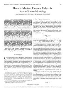
A. The bare SISD core The SISD model is a non-pipelined RISC system with 8 general-purpose registers, as well as dedicated special registers such as the Program Counter (PC), the Instruction Register (IR), Memory Address Registers (MAR) and Memory Data Registers (MDR). Attempting to make the most out of available FPGA resources, dedicated Block RAM resources are chosen to serve as Instruction Memory (IM) and Data Memory (DM) of the SIxD (Fig. 1). The Register File (RF) with a single-port input and a double-port output has been implemented as Select RAM in the FPGA. The primitive Hardware Multiplier, which is standard in Xilinx Virtex and Spartan 3 FPGAs, is the obvious choice for multiplier, requiring no LUT space on the chip. If no Hardware Multiplier is present on the target FPGA, the user must either remove the multiplication instruction or provide with a custom generic multiplier. The hardwired Control Unit (CU) is a Finite State Machine implementing a sequential circuit based on different states of the machine, issuing a set of control signals at each
Instruction Memory. There is no stack or accumulator on the SIxD, resulting in a single level of interrupt handling. TABLE I. Opcode 0000 0001 0010 0011 0100-0110 0111 1000 1001 1010-1011 1100-1101 1110 1111
THE SIXD INSTRUCTION SET
Explanation NOOP-enable/disable interrupts-RET a
A/L register (direct) a A/L register (immediate) a A/L register (indirect) Reserved Shift/Rotate right/left Multiply SIMD: execute instruction Load/store to/from memory Branch if less than/branch if equal to SIMD: load/store/route/set_iter Immediate/indirect load/store from/to memory/port
~b 2 4 4 5 4 4/5 -c 3 5 -c 2/3/4
a. A/L: Arithmetic/Logic (ADD/SUB/AND/OR/XOR). b. ~: clock cycles. c. See Table III.
Figure 1: The SISD datapath
state. Depending on the instruction word input, the Control FSM completely describes the Instruction Set Architecture of the SIxD, by setting up the necessary bits for corresponding units to perform the correct operation. The instruction formats supported by the SIxD are: • • • •
Register-register (direct) Register-constant (immediate) Register-memory (indirect) Branching format
A custom unit can be a user-defined instruction or a custom-designed hardware module. The bare SISD core has an ALU, a multiplier and no custom unit. In order to create a custom instruction on the SISD, the custom unit must be placed with input(s) from the Register File, and output(s) to the RF input multiplexer. A reserved opcode in the ISA must be associated with the control on the new unit and corresponding states must be revised for the proper enabling of the unit, and the correct choice of the select signal of the RF input multiplexer to assure the proper propagation of the outputs. The reserved places are used for custom instruction extension to the ISA. More custom units could be added to the ISA by having selection bits distinguish different instructions, like done in the shift instructions; two instructions in a single opcode, distinguished by an unused bit or field of the instruction word. Up to four interrupts are implemented, as well as an interrupt enable/disable instruction. The SIxD gives an exception when an invalid opcode is read. The interrupt/exception addresses are at the start of the
B. The Configuration File Although Table I shows the full instruction set, it should be noted that these instructions can be modified during the synthesis of the core with the aid of a configuration file written in VHDL. The following types of modifications are supported by the configuration file: 1) Enable SIMD with a number of Processing Nodes: Depending on the size of chip, the user can enable SIMD instructions, choosing to have any number of Processing Nodes (PN) that is a multiple of two. 2) Determine the data space (width and length): Depending on the size of data memory needed and the Block RAM available on the FPGA, the user can specify the data width as a multiple of 8 bits, and data length (at least 2K words). 3) Select the most appropriate branching and shifting instructions: In the default instruction set, BL and BEQ are used. However, if greater-than operations are used more frequently than BL, then the user has the chance of replacing BL with BG. There are six possible branch instructions for two branch instruction slots: BEQ, BNEQ, BL, BLEQ, BG, and BGEQ. As for the shift instructions, arithmetical, logical shift or rotation operation can be inserted into the ISA. 4) Remove unused instructions from the instruction set: As an example, removing the 16-bit XOR instruction would reduce the area of the ALU by 11 slices (Table II). This way, the SISD core can fit in a very small FPGA.
TABLE II. Unit SISD (all) ALU Register File Reg. MUX Control Unit
SISD SLICE INFORMATION
Memory to read from when writing back to the main Data Memory.
Data Width 8-bit
279 68 20 22 186
16-bit
426 148 40 44 186
24-bit
573 231 60 66 186
32-bit
689 310 80 88 186
C.
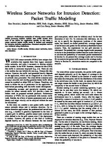
The SIMD functionality The SIMD functionality of the SIxD, depicted in Fig. 2, is initiated within the configuration file by the SIMDenable signal set high. This produces the generation of a number of user-defined Processing Nodes. A SIMD Processing Node is made up of a Local Memory (depicted as LM, a dual-ported Block RAM) and a Processing Element (PE), thus providing with the most elementary units for computation. The Local Memory (SIMD registers) also needs to be able to take inputs from the main Data Memory, resulting in a need for a multiplexer, completing the PN. The instructions that emerge with the activation of the SIMD are as shown in Table III. For these SIMD instructions, only register indirect addressing can be used, otherwise there would be no way of issuing a SIMD instruction inside a 16-bit instruction word. In these instructions, the register contents act as address locations for the DM and the LMs. The set_iter instruction sets an iterations register, iter, with a constant, determining the number of times to repeat the given SIMD instruction. Let’s say that a load vector instruction is being issued on the SIMD with 4 processing elements, and iter is set to 8. In this case, 32 values inside the DM are distributed dually (via dual-port Block RAMs) to 8 consecutive locations in the 4 PEs. This way, the iterations register achieves the speeding up of data transfers between the DM and the LMs. A large data multiplexer is placed at the output to select which Local
For the SIMD part, the customization process differs in the sense that the new functional unit is added inside the Processing Element with a certain bit of the op_sel signal enabling it. For a single-cycle custom operation, no other modification of the core is necessary. If the custom unit outputs two results, setting the double_output bit high on the configuration file lets results to be written on two consecutive memory address locations. TABLE III. SIMD instruction
~b
Explanation
Load vector
Loads a vector from DM to the LMs.
5+3i
Store vector
Stores a vector from LMs to the DM.
5+3i
Exec. vector
Execute two vectors based on the op_sel signal, save to a vector in LMs.
6+2i
Route
Route a scalar from one LM to another.
9
Set_iter
Set the number of iterations to perform.
2
a a a
a. i: iterations. b. ~: clock cycles
D. Intra-PE Communications It is easy to implement a SIMD with communication autonomy [6]; by having the LM input multiplexers (Fig. 2) take their inputs from all outputs of all PEs. Of course, this results in very large multiplexers and increased area usage. If an on-chip network is formed with routers in-between the LMs, these multiplexers can be removed. The slow but small method implemented in the SIxD employs none of these, but uses a pre-defined look-up table that contains encoded direction information for the movement of data between the LMs. The table consists of encoded bits of source and destination PEs, requiring no extra hardware, and only a few slices. For example, if the user defines “101” as a transfer from LM1 to LM4 in compile-time, using this bit sequence inside the “route” instruction, along with the source LM address and the destination LM address results in a data movement between these two Processing Units. The size of the SIMD is completely dependent on the application, since the number and the contents of the Processing Elements determine the size of the SIMD mode of the SIxD core. Section III gives better insight on the utilization and performance of the core with an implementation of MPEG-7 Motion Activity Descriptors on the SIxD. III.
Figure 2: The SIMD unit
SIMD INSTRUCTIONS OF THE SIX D
IMPLEMENTATION EXAMPLE: THE MPEG-7 MOTION ACTIVITY DESCRIPTORS Although a detailed explanation can be found in [7], The MPEG-7 Motion Activity Descriptors (MAD) considered here are for motion intensity and spatial distribution of motion activity. The algorithm can be summarized as
follows: In a set of motion vectors, first the hypotenuses of 8-bit input pairs are calculated, and the average of the results are found. The spatial activity matrix is calculated by setting the values lower than the average to zero. Another averaging of this matrix gives the intensity of motion for the frame. The descriptor implementation which works with pre-calculated motion vectors has been employed on 16x16 motion vectors, requiring two sets of 256 elements each. Although the inputs are 8-bits wide, a 16-bit CPU was used because of the usage of multiplication and averaging. For the sake of processing comparison, data is previously loaded from the input ports, and is available in Data Memory. There are many ways to implement this “take-thehypotenuse/square root-and- accumulate- intensive” application. On the SISD, an 8-bit square root calculation takes about 280 clock cycles. A custom unit designed for this calculation and placed in opcode “0100” takes 5 cycles and 55 slices to compute the square root. The whole algorithm runs for a total of 21,286 clock cycles. Another method is to use a specially-designed hypotenuse unit, taking 76 slices, and 5 clock cycles to execute. Using this unit that has two MUL, one ADD, and one SQRT operation combined into one HYP instruction, the total MAD runtime takes 19,413 clock cycles. Finally, enabling the SIMD and using vector instructions on specially designed PEs that execute in two clock cycles and occupying 111 slices, the results are shown in Table IV. THE MPEG-7 MOTION ACTIVITY DESCRIPTOR ON THE SIXD
TABLE IV.
No. PN
Iter
Total slices
SIMD slices
Max. freq. (MHz)
Runtime (clock cycles)
Power cons. (mW)
2
128
963
475
109
1833
521
4
64
1205
717
94
1196
548
8
32
1647
1163
94
882
542
16
16
2523
2049
89
734
566
32
8
4266
3800
94
678
606
64
4
7754
7288
83
686
647
Fig. 3 shows the PE designed for the SIMD execution of the algorithm, and how the PE operation bits were used to manage the units. First the hypotenuses are calculated in parallel on all PNs, while the outputs are collected and added by the accumulator. Then, the final accumulator results are gathered by the SISD, added and shifted to compute the average, and sent back to the PNs of the SIMD. Afterwards, the compare instruction comes into play, comparing the data elements with the average, outputting zero if less than the average, or the input data itself if greater than or equal to the average, forming the spatial activity matrix. Meanwhile, it also accumulates its results, which are finally saved, added and scaled together for the final result, the intensity of motion for the frame.
Figure 3: The Processing Node for the MPEG-7 Motion Activity Descriptor and the PE operation table.
When the chosen number of Processing Nodes of the SIxD is redundant for the algorithm, the design not only takes up too much space, but is slower and inefficient: Experiments done with 128 and 256 PEs resulted in 14,780 and 28,720 total slices and 762 and 944 clock cycles to execute, respectively. This is due to the fact that the data transfer starts taking more time than the processing. The ideal number of PNs is 16 or 32 for the Motion Activity Descriptor on a 16x16 motion vector frame, depending on area or time being a constraint. Furthermore, the 256-PE SIMD doesn't fit even fit the biggest Xilinx Virtex-II chip (8M gates), occupying 259 Block RAM and 513 MUL units. IV. CONCLUSIONS In this study, we have implemented a flexible application-specific soft processor that can be configured to run in scalar mode and fit in small FPGAs or run with vector processing (SIMD) capability for higher performance on larger chips. We have demonstrated an implementation of the core with the MPEG-7 Motion Activity Descriptors, showing how the core might be configured for up to 28-fold speedup in algorithm run time. In the future, the core’s flexibility is to be further tested with more complex algorithms. REFERENCES [1] [2] [3] [4] [5]
[6]
[7]
MicroBlaze Processor Reference Guide, Xilinx Inc. http://www.xilinx.com/ise/embedded/mb_ref_guide.pdf. Nios Embedded Processor, Altera Inc. http://www.xilinx.com/ise/embedded/mb_ref_guide.pdf. R.E. Gonzalez, "Xtensa: A Configurable and Extensible Processor, " IEEE Micro, vol. 20, no. 2, pp. 60-70, Mar. 2000. Freedom CPU, http://f-cpu.seul.org/. D. Etiemble and L. Lacassagne, "Introducing image processing and SIMD computations with FPGA soft-cores and customized instructions", in 1st International Workshop on Reconfigurable Computing Education, Karlsruhe, Germany, March 2006. P. J. Narayanan, "Processor Autonomy on SIMD Architectures," In Proc. the ACM International Conference on Supercomputing, pp. 127--136, July 1993. Savakis A, Sniatala P, Rudnicki R. “Real-time video annotation using MPEG-7 motion activity descriptors,” Conference MIXDES 2003. Lodz: June 26-28: 2003.