layer was deposited by spin coating at 3000 r/min for 60 s at ambient .... 228â229. [11] W. Zhu, T. P. Ma, T. Tamagawa, Y. Di, J. Kim, R. Carruthers, M. Gibson,.
IEEE ELECTRON DEVICE LETTERS, VOL. 27, NO. 8, AUGUST 2006
653
SONOS-Type Flash Memory Using an HfO2 as a Charge Trapping Layer Deposited by the Sol–Gel Spin-Coating Method Hsin-Chiang You, Tze-Hsiang Hsu, Fu-Hsiang Ko, Jiang-Wen Huang, Wen-Luh Yang, and Tan-Fu Lei
Abstract—In this letter, the authors fabricate the silicon–oxide–nitride–oxide–silicon (SONOS)-like memory using an HfO2 as charge trapping layer deposited by a very simple sol–gel spin-coating method and 900 ◦ C 1-min rapid thermal annealing. They examine the quality of sol–gel HfO2 charge trapping layer by X-ray photoemission spectroscopy, Id–V g, charge retention, and endurance. The threshold voltage shift is 1.2 V for the sol–gel HfO2 trapping layer. The sol–gel HfO2 film can form a deep trap layer to trap electrons for the SONOS-like memory. Therefore, the sol–gel device exhibits the long charge retention time and good endurance performance. The charge retention time is 104 s with only 6% charge loss and long endurance program/erase cycles up to 105 . Index Terms—Charge retention, endurance, HfO2 , sol–gel spin coating, silicon–oxide–nitride–oxide–silicon (SONOS)-like memory.
I. I NTRODUCTION
R
ECENTLY, silicon–oxide–nitride–oxide–silicon (SONOS)type memory is widely used for nonvolatile memory (NVM) like electrically erasable programmable read-only memory (EEPROM) and flash memory. SONOS-like memory can have a better charge retention than floating-gate memory when floating-gate bitcell’s tunneling oxide is below 10 nm or a large number of megabit arrays are evaluated due to its spatially isolated deep-level traps, so a single defect in the tunneling oxide will not cause the discharge of the memory cell [1]–[6]. The charge trapping layer of traditional SONOS memory is silicon nitride (Si3 N4 ). High-κ materials are being considered as charge storage materials to get faster programming speed and better charge retention performance. In comparison with Si3 N4 film, HfO2 film has been reported a reduced overerase phenomenon and self-limiting charge storage behavior under both erase and program operations [1]. Recently, numerous technologies [1]–[6] have been developed for the preparation of various high-κ films. To prepare insulating thin films, atomic
Manuscript received April 7, 2006; revised May 31, 2006. The review of this letter was arranged by Editor C.-P. Chang. H.-C. You, T.-H. Hsu, and T.-F. Lei are with the Institute of Electronics Engineering, National Chiao-Tung University, Hsinchu 300, Taiwan, R.O.C. F.-H. Ko and J.-W. Huang are with the Institute of Nanotechnology, National Chiao-Tung University, Hsinchu 300, Taiwan, R.O.C. (e-mail: fhko@mail. nctu.edu.tw). W.-L. Yang is with the Department of Electronic Engineering, Feng Chia University, Taichung 407, Taiwan, R.O.C. Digital Object Identifier 10.1109/LED.2006.879026
layer deposition (ALD), physical vapor deposition (PVD), and chemical vapor deposition (CVD) methods have all been used to prepare films for new technologies. The sol–gel method is a very interesting and simple technique for preparing ceramic films [7]. However, no reports exist that describe the fabrication of SONOS-like memory by utilizing the sol–gel spin-coating method. The sol–gel method [8] can mix colloidal solvents and precursor compounds when metal halides are hydrolyzed under controlled conditions. In the sol–gel process [8], hydrolysis, condensation, and polymerization steps occur to form metal oxide networks. These reactions play crucial roles in modifying the final material’s properties. The most interesting feature of sol–gel processing is its ability to synthesize new types of materials that are known as “inorganic–organic hybrids.” The film formation with a spin coating is a more simple method than ALD, PVD, or CVD due to its cheaper precursor and tool. In addition, the film can be fabricated in the normal pressure system instead of high-vacuum system. In this letter, we use the novel sol–gel spin-coating HfO2 thin film as a charge trapping layer to fabricate the SONOS-like memory. II. E XPERIMENTAL The fabrication of a sol–gel spin-coating high-κ SONOS memory is started with a local-oxidation of silicon (LOCOS) isolation process on p-type (100) 150-mm silicon substrate. At the beginning, a 4-nm tunneling oxide was thermally grown at 925 ◦ C by furnace oxidation. HfO2 charge trapping layer was prepared using a sol–gel spin-coating method. HfCl4 (99.5%, Aldrich, USA) was used as the precursor for the synthesis of hafnia. A mother sol solution was first prepared by dissolving HfCl4 in isopropanol (IPA; Fluka; water content < 0.1%) under vigorous stirring in an ice bath. The sol solution was obtained by fully hydrolyzing HfCl4 with a stoichiometric quantity of water in IPA to yield a Hf:IPA molar ratio of 1:1000. HfO2 layer was deposited by spin coating at 3000 r/min for 60 s at ambient temperature (25 ◦ C). The spin coater used was TEL Clean Track Model-MK8 (Japan). After spin coating, the wafer was under rapid thermal annealing (RTA) at 900 ◦ C for 60 s in O2 ambient to form HfO2 . The film thickness was about 20 nm measured by ellipsometer. The 30-nm-thick blocking oxide was deposited by low-pressure chemical vapor deposition (LPCVD) tetraethoxysilane (TEOS). Prior to deposit 200-nm poly-Si gate, the TEOS oxide was densified in N2 ambient
0741-3106/$20.00 © 2006 IEEE
654
IEEE ELECTRON DEVICE LETTERS, VOL. 27, NO. 8, AUGUST 2006
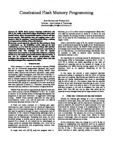
Fig. 1. Sol–gel SONOS-like memory structure and the ideal band diagram.
Fig. 2. XPS spectra of as-deposited and 900 ◦ C RTA sol–gel HfO2 films. Fig. 3. (a) Id–V g curve of the sol–gel SONOS-like memory. (b) The program speed of the sol–gel SONOS-like memory.
under 900 ◦ C for 30 s anneal to repair the defects and decrease the number of traps. Finally, gate pattering, source/drain (S/D) implant, and the rest of the subsequent CMOS processes were used to fabricate this SONOS-like memory. Fig. 1 depicts the schematic structure of our device and the basic band diagram from the literature [1]. III. R ESULTS AND D ISCUSSION In order to analyze the chemical composition of hafnia film, elements are detected by X-ray photoemission spectroscopy (XPS). Fig. 2 demonstrates the high-resolution spectrum of Hf 4f peak for the sol–gel film. The Hf 4f7/2 peak was approximately 16.8 eV with a difference of 1.7 eV in binding energy between the Hf 4f5/2 and Hf 4f7/2 peaks at RTA treatment temperature of 900 ◦ C. This observation suggests the sol–gel film is HfO2 and is similar with the literature identification for HfO2 film from ALD method [9]. From the Hf 4f spectrum, we observe clearly RTA annealing under 900 ◦ C in O2 treatment leads to remarkable changes in the XPS spectra. This change, which is apparent from the increase in the signal of the Hf–O bonds upon increasing the annealing temperature. The as-deposited hafnia film is mainly HfO2−δ (δ > 0), while the annealing under oxygen ambient can decrease the δ value. This finding indicates that structural composition of the HfO2 has occurred. Fig. 3(a) shows the Id–V g curve of the SONOS memory. We use channel hot electron injection to program, and band-to-
band tunneling induced hot-hole injection (BTBHHI) to erase. The program condition is V g = 12 V, V d = 10 V for 1 ms. The erase condition is Vg = −12 V, V d = 10 V for 1 ms. We can read the Vth shift (= “Vth of program” − “Vth of erase”) about 1.2 V from Fig. 3(a). The subthreshold slope of Id–V g curves are different for the fresh cell and erased cell. The degradation of the subthreshold swing of the device with localized charge trapping is attributed to a subsurface conduction underneath the charge trapping region [10]. The program speed is shown in Fig. 3(b). We list three different stress conditions: Vg = 10, 12, 15 V; V d = 10 V. As Fig. 3(b) shows, the condition Vg = 12 V and V d = 10 V at 1 ms causes V to shift 1.2 V. With increasing the Vg, the Vth shift also increases and the program speed becomes faster. It is noted that only 10 µs for the condition of Vg = 15 V and V d = 10 V to shift Vth of 1 V. We think Vth shift is due to the electron trapping in the HfO2 layer. The band offset is the reason why trapping occurred. Fig. 1 is the typical band diagram for the HfO2 SONOS-like memory [1]. The conduction band offset is 1.5 eV between HfO2 and p-Si substrate. During programming, the electrons in the substrate gain energy from the applied voltage of Vg and Vd. If the energy is enough to cross the 3.1 eV potential barrier, the hot electrons will across the thin tunneling oxide to the HfO2 charge trapping layer and be trapped. This causes the Vth change. The valence band offset is 3.1 eV between HfO2 and p-Si substrate. When erasing, we apply a negative gate voltage and positive drain voltage to
YOU et al.: SONOS-TYPE FLASH MEMORY USING AN HfO2 AS A CHARGE TRAPPING LAYER
Fig. 4.
655
Charge retention curve of sol–gel HfO2 SONOS-like memory. Fig. 5. Endurance characteristics of sol–gel HfO2 SONOS-like memory.
generate hot hole in the substrate. If the hot hole in the substrate achieves enough energy to cross the 4.6 eV energy barrier, it can reach the HfO2 charge trapping layer and cause the Id–V g curve shift toward left. We can see the erase Id–V g curve cannot match with the fresh Id–V g curve from Fig. 3. This reason is because some electrons are trapped in the deep trap level of HfO2 , and are hard to be released. Hence, the deep trap is beneficial for the sol–gel memory work. Fig. 4 is the charge retention characteristics of HfO2 SONOS-like memory measured at the room temperature. We find the small charge loss with time in the sol–gel SONOS-like memory. The curve shows only 6% charge loss as measured time up to 104 s. We infer this contribution is from the electron deep trap of sol–gel HfO2 charge trapping layer mentioned above [3], [11]. The endurance of the sol–gel HfO2 SONOS-like memory is shown in Fig. 5. The measured condition is—program: Vg = 12 V, V d = 10 V, 1 ms; erase: Vg = −12 V, V d = 10 V, 1 ms. A very small increase of the erase Vth is observed from the figure. In addition, no significant window narrowing is observed. This observation is due to the formation of deep trap level that makes it hard to erase all trapped electrons. After 105 program/erase (P/E) cycles, the memory window is still fixed around 1.2 V. This finding suggests the simple sol–gel process can be incorporated into the SONOS-like memory fabrication. IV. C ONCLUSION In this letter, we propose a new spin-coating method to deposit charge trapping layer for SONOS-like memory. We have shown the electric curves, like Id–V g, charge retention, and endurance, which can demonstrate the quality of sol–gel spin-coating high-κ layer with some satisfactory characteristics in terms of 1.2 V memory window, long charge retention time
due to deep trap level in the HfO2 layer, and good endurance up to 105 P/E cycles with no memory window narrowing. R EFERENCES [1] Y. N. Tan, W. K. Chim, B. J. Cho, and W. K. Choi, “Over-erase phenomenon in SONOS-type flash memory and its minimization using a hafnium oxide charge storage layer,” IEEE Trans. Electron Devices, vol. 51, no. 7, pp. 1143–1147, Jul. 2004. [2] Y. N. Tan, W. K. Chim, W. K. Choi, M. S. Joo, T. H. Ng, and B. J. Cho, “High-κ HfAlO charge trapping layer in SONOS-type nonvolatile memory device for high speed operation,” in IEDM Tech. Dig., 2004, pp. 889–892. [3] T. Sugizaki, M. Kohayashi, M. Ishidao, H. Minakata, M. Yamaguchi, Y. Tamura, Y. Sugiyama, T. Nakanishi, and H. Tanaka, “Novel multi-bit SONOS type flash memory using a high-κ charge trapping layer,” in VLSI Symp. Tech. Dig., 2003, pp. 27–28. [4] X. Wang and D. L. Kwong, “A novel high-κ SONOS memory using TaN/Al2 O3 /Ta2 O5 /HfO2 /Si structure for fast speed and long retention operation,” IEEE Trans. Electron Devices, vol. 53, no. 1, pp. 78–82, Jan. 2006. [5] B. D. Salvo, C. Gerardi, R. van Schaijk, S. A. Lombardo, D. Corso, C. Plantamura, S. Serafino, G. Ammendola, M. van Duuren, P. Goarin, W. Y. Mei, K. van der Jeugd, T. Baron, M. Gely, P. Mur, and S. Deleonibus, “Performance and reliability features of advanced nonvolatile memories based on discrete traps,” IEEE Trans. Device Mater. Rel., vol. 4, no. 3, pp. 377–389, Sep. 2004. [6] M. H. White, D. A. Adams, and J. Bu, “On the go with SONOS,” IEEE Circuits Devices, vol. 16, no. 4, pp. 22–31, Jul. 2000. [7] H. C. You, F. H. Ko, and T. F. Lei, “Physical characterization and electrical properties of sol-gel-derived zirconia films,” J. Electrochem. Soc., vol. 153, no. 6, pp. F94–F99, 2006. [8] C. J. Brinker and G. W. Scherer, Sol-gel Science. San Diego, CA: Academic, 1989. [9] Y. Won, S. Park, J. Koo, S. Kim, J. Kim, and H. Jeona, “Initial reaction of hafnium oxide deposited by remote plasma atomic layer deposition method,” Appl. Phys. Lett., vol. 87, no. 26, p. 262 901, Dec. 2005. [10] Y. Wang, Y. Zhao, B. M. Khan, C. L. Doherty, J. D. Krayer, and M. H. White, “A Novel SONOS nonvolatile flash memory device using hot hole injection for write and tunneling to/from gate for erase,” in Proc. ISDRS, 2003, pp. 228–229. [11] W. Zhu, T. P. Ma, T. Tamagawa, Y. Di, J. Kim, R. Carruthers, M. Gibson, and T. Furukawa, “HfO2 and HfAlO for CMOS: Thermal stability and current transport,” in IEDM Tech. Dig., 2001, pp. 463–466.