The focus of our research has been operable memory tags suitable for cons ubimedia applications. The tag is develop mobile-phone-centric architecture. Ou.
UBICOMM 2010 : The Fourth International Conference on Mobile Ubiquitous Computing, Systems, Services and Technologies
System Architecture for Mobile-phone-readable RF Memory Tags Iiro Jantunen, Jyri Hämäläinen, Timo Korhonen
Harald Kaaja, Joni Jantunen, Sergey Boldyrev
Department of Communications and Networking Aalto University Espoo, Finland {iiro.jantunen, jyri.hamalainen, timo.korhonen}@tkk.fi
Nokia Research Center Helsinki, Finland {harald.kaaja, joni.jantunen, sergey.boldyrev}@nokia.com
Abstract — We have developed an open architecture platform for implementing passive radio-frequency identification (RFID) tags with a mass memory. Purposes for such mass memory tags are, e.g., multimedia files embedded in advertisements or logged sensor data on a low-power sensor node. In the proposed architecture, a mobile phone acts as the reader that can read or write the memory of these RFID tags. The architecture is designed so that development path to a full Network on Terminal Architecture (NoTA) is feasible. The wireless reading speed of the mass memory tags, demonstrated to be 112 Mbit/s, is in range that a 3-minute VGA size video can be loaded from the tag to the phone in less than 10 s. Keywords — Memory architecture; Multimedia systems; RFID; telephone sets; RF memory tags
I.
INTRODUCTION
RFID tags are increasingly a part of our life; transport, traceability, and secure access are some of the main uses of this technology today. Conventional machine-readable wireless tags, e.g., Near Field Communication (NFC) tags, normally have a very small memory in range of hundreds of bytes or kilobytes. Some RFID standards include an option to have a flexible-use memory, but the capacity is low compared to factory-set fixed-content memory. Tag selection is based on reading the content in a selected tag memory address (e.g., tag or manufacturer ID). As the memory capacity of these tags is small, the amount of data to be transferred is also small and power consumption of RF communication is, thus, not a critical issue. To overcome the storage capacity limitation of passive tags, Wu et al. increase effective tag storage sizes with proposed distributed RFID tag storage infrastructure (DRFID stores) [1]. Ahmed et al. focus on RFID system unreliability and improvements in middleware for object tracking and object location with moving readers or tags [2][3]. Ying described a verification platform for RFID reader that utilized Ultra High Frequency (UHF) frequency [4]. Pillin et al. have developed a passive far-field RFID tag using the 2.45 GHz Industrial, Scientific and Medical (ISM) band, with a data rate of 4 Mbit/s on the range of 5.5 cm [5]. As an example of a proprietary solution, HP’s Memory Spot RFID tag also works on the 2.45 GHz band and has demonstrated 4 MB memory and 10 Mbit/s data rate [6]. Today’s mobile phones provide music and video players, which make it possible for consumers to enjoy entertainment while on the move. Acquiring new multimedia content by downloading or streaming, however, is hampered by the high cost and slow speed of Internet connections, as well as by the
Copyright (c) IARIA, 2010
ISBN: 978-1-61208-100-7
fact that commonly used physical multimedia formats, such as optical disks, cannot be read with a mobile phone. Thus, to make acquiring new content easier, cheaper and less power-consuming, we propose a new technology based on RF memory tags readable and writable by mobile phones. The problems of low data reading rate and small memory size provided by contemporary RFID tags become emphasized if one considers mobile users reading multimedia files from tags embedded on, e.g., paper media. The attention span of a mobile user is about 10 seconds [7]. Within this period, the user could get a single multimedia content file from a memory tag. Considering a movie trailer, the file size for a 2-minute 640×320-pixel 30-fps (3 Mbit/s), encoded with H.264, would be in range of 50 MB [8]. The required minimum data transfer rate from the user point-ofview is thus 50 Mbit/s. This exceeds the maximum data rate available by 13.56 MHz NFC technology, 848 kbit/s, by a factor of 60. Even the maximum data rate for NFC demonstrated on a laboratory set-up, 6.78 Mbit/s [9], is not enough. Thus, there is a need for a new high-speed touchrange RFID radio interface. The aim of our research has been to develop a highcapacity memory tag, which is wirelessly readable with a mobile phone and suitable for consumer markets in ubimedia applications [10][11]. The mobile phone acts as the user interface for reading and writing passive RF memory tags that contain a high-capacity memory (0.1–1 GB). The reasoning for the proposed technology was justified by modern trends in non-volatile memory technologies, according to which the power consumption, physical size, and price of memory are continuously decreasing. In this paper we describe and specify a network architecture, which enables mobile phones to read and write passive RF memory tags. The architecture has been developed and demonstrated in the EU's 6th Framework Programme (FP) “Micro-Nano integrated platform for transverse Ambient Intelligence applications” (MINAmI) project [12], and thus the architecture is referred to as MINAmI Architecture. Important architecture requirements include openness, modularity, scalability, and energy efficiency. Openness and modularity are needed to support creation of novel applications and services by 3rd parties. Scalability of data rate is needed to enable evolution of the technology along with evolution of multimedia services. Energy efficiency is essential to enable passive operation of the tags as well as to save the phone’s battery. The paper is organized as follows. In Section II, we introduce the system architecture, along with a key component of the architecture, RF memory tags. In Section
310
UBICOMM 2010 : The Fourth International Conference on Mobile Ubiquitous Computing, Systems, Services and Technologies
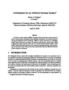
Figure 1. MINAmI Architecture
III we introduce a novel dual-band band radio subsystem and its hardware and software implementation. In Section IV, we present the current status of implementation of the architecture and discuss possibilities for future deve development. Section V concludes the paper. II.
MINAMI ARCHITECTURE
The proposed MINAmI architecture makes use of the mobile phone’s capability of running software and providing several radio interfaces (Figure 1 [11]). ). The archite architecture is modular, enabling simpler and faster development of new technical extensions (e.g., RF memory tags). Our architecture focuses on utilization of modularity on component level (e.g., where to plug memory tag functionality) and on communication level (e.g., how the available memory tags are utilized). ). At short proximity domain (range < 1 m), different tags are communicating locally with a mobile phone. In the present work we have concentrated on the RF memory tags. The sensor parts of the architecture (RFID sensor tags and Bluetooth sensor devices) have been studied in an earlier project [13][14]. [13] The main RF memory tag architectural design challenges include target platform performance obstacles, such as available bus operations (R/W) and power requirements, especially when drawing the line for autonomous operations in described escribed MINAmI architecture. The other challenge is minimizing changes to the existing system communication layering, only to the external memory stack block. The choices in the MINAmI system architecture were able to support both existing standard radioss for low-rate low sensors, and the high-rate high-capacity capacity memory tags. A. Network-on-Terminal Terminal Architecture (NoTA) NoTA is modular service-based based system architecture for mobile and embedded devices offering services and applications to each other. The concept is being defined in an open initiative, in NoTA World [15].. NoTA is also known as an open device distributed architecture, which allows direct connections between different nodes, within subsystem or between subsystems. This architecture supports both bot messaging and streaming services. The beauty in the architecture resides in modularity and transport independency. Direct connection between subsystems improves the efficiency as they do nott necessarily require any processor involvement, when subsystems have all the needed functionalities available for their independent operations. Transport-specific specific portion is hidden underneath NoTA communication layering.
Copyright (c) IARIA, 2010
ISBN: 978-1-61208-100-7
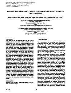
Figure 2. NoTA extension architecture for MINAmI subsystem, where HSI - High Speed Serial Interface; HS-MMC HS - High Speed MultiMediaCard: SPI - Serial Peripheral Interface bus.
NoTA communication layering is built around transportindependent parts and interfacing towards transport-specific tra parts (Figure 2). ). Device Interconnect Protocol (DIP) provides logical links between a requesting subsystem and other subsystems or within a subsystem.[15]. DIP is a device-level level communication protocol that can be implemented for various physical interfaces ranging from MIPI (Mobile Industry Processor Interface) high speed serial interfaces and Universal Serial Bus (USB) ( to wireless interfaces, such as Bluetooth [16][17]. NoTA host subsystem and neighboring subsystems are connected via the high speed physical interface. DIP adapts physical interfaces to the upper layers. It is the lowest layer that is common for all subsystems (i.e., also for MINAmI subsystem) and hides the physical dependencies underneath. Above DIP there is a common service interface used for resource management, file systems, and system boot-ups. boot Middleware frameworks, e.g., for multimedia, USB, and other applications, use a common service interface or extension Application Programming Interface (API). The T architecture also takes into account vertical solutions, which may require an optimized protocol design for certain requirements that are tied to HW-specific HW applications. NoTA subsystem structure takes into account possibility to add different types of independent (service/application) subsystems to the architecture, and MINAmI architecture forms one high data rate high gh capacity subsystem. subsystem MINAmI subsystem offers memory tag read/write, storage and local connectivity services to other subsystems within mobile device,, and its architecture is compatible with NoTA communication layering. layering MINAmI subsystem includes both the mobile phone (Mobile Reader/Writer) and the tag and all the relating hardware and software resources. Mobile Reader/Writer sees the contents conte of the memory of a passive RF memory tag only when there is an established connection, i.e., power field and data connection exists. B. RF Memory Tags The focus of our research has been on mobile-phonemobile operable memory tags suitable for consumer markets and ubimedia applications. The tag is developed as a part of our mobile-phone-centric centric architecture. Our memory tag
311
POWER MANAGEMENT
HSI
UBICOMM 2010 : The Fourth International Conference on Mobile Ubiquitous Computing, Systems, Services and Technologies
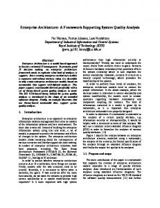
Figure 3. MINAmI Architecture on phone
development targets improving both transfer tran speed and storage capacity. These improvements give direct benefit for ubimedia users. The target memory capacity of our memory tag has been in the range of gigabits and mobile reader/writer transfer speed to and from memory tag in excess of 10 Mbit/s. Mbit/ The same design platform is usable for both ends, for mobile phone platform reader/writer and for tag implementation. When designing the platform, various important design parameters, such as the selection of the used radio technology, were considered to provide an efficient and low lowpower solution for mobile reader/writer and tags. It was important to make sure that connectivity technology is simple enough for the user, e.g., it should facilitate easy content selection (see Section III.D). Memory tag content selections should be based on metadata (e.g., filenames, file content types, file content keywords). Due to the large rge memory size, power consumption for memory access is a critical design issue, both for reading and writing the memory tag. To be successful on the market, RF memory tags for ubimedia must be passive to make them as small (size) and cheap as possible, and d to achieve autonomous usage with minimum maintenance (e.g., (e.g. usage without charging of battery). This severely limits the power budget. On the other hand, a short communication range (even touch) is sometimes preferable to make it easier for the user to physically hysically select the tag. An RF memory tag will be read many times by different users, but written more rarely – in some cases, only once. The memory unit must work reliably even with several consecutive read cycles. A limited write throughput due to power constraint is not an issue, as data is rarely written by the users. III.
UWB LOW END EXTENSION
As memory tags have high data storage capacity, a highhigh speed radio is needed for communication to enable reading even alll the contents of the tag in an acceptable time. Currently available mobile phones contain several radio transceivers, such as cellular, Bluetooth, and Wi-Fi, Wi along
Copyright (c) IARIA, 2010
ISBN: 978-1-61208-100-7
Figure 4. MINAmI Architecture on a RF memory tag
with NFC. Most of the technologies are made for well wellestablished communication between active acti devices, consuming a relatively large amount of power. These technologies are also not inherently designed for ad-hoc, ad possibly one-time, time, connections between devices that have not communicated with each other before, resulting in long latency in establishing shing the communications. For example, in an environment with many unknown Bluetooth devices, the Bluetooth connection setup latency can be over 10 seconds [18]. NFC C enables communications between an active and a passive battery-less less device and is physically more selective; its communication range is almost in touch. However, it has severe limitations in data transfer speed. To provide higher data rates, a wider frequency fre band available on higher frequencies needs to be used. On the other hand, the efficiency of wireless power transfer (WPT) decreases as a function of center frequency. To solve the problem of providing high-speed high communication (high frequency needed) while simultaneously providing power wirelessly to the tag, a dual-band dual radio interface has been proposed [19].. One narrowband signal on RFID frequencies (e.g., RFID FID frequency bands globally available between 860–960 960 MHz) is used to power the tag and to provide a mutual clock reference for both ends of the communication link, whereas the communication link itself is based on impulse UWB technique to provide a high communication bandwidth and scalability for even higher data rates. As the selected RFID frequencies are approximately in the same frequency range as GSM/WCDMA 900 MHz, in the reader there is a possibility of integrating the WPT function to the existing Ph Phone Radio Subsystem, as presented in Figure 3.. In that case, Phone Radio Subsystem is designed so that the WPT Physical (PHY) Layer function may request a direct access to control the activation of the narrowband transmitter. Especially, the time-domain time interleaving of different functions is important to support coco existence of GSM/WCDMA and WPT signaling. The architecture of the RF memory tag (Figure 4) is similar to the MINAmI subsystem on the mobile phone. For simple RF memory tags, no network layer implementation is needed to take care of the point point-to-point communication between the reader and the tag, and therefore is handled on Medium Access Control (MAC) layer. As an option for use-cases cases like data data-logging sensor devices, the memory control layer provides a sensor interface. During the sensing, the sensor data is stored to the
312
UBICOMM 2010 : The Fourth International Conference on Mobile Ubiquitous Computing, Systems, Services and Technologies
Phase-Change Memory (PCM) block and the low data-rate data capturing is powered from a battery or with energy harvested from the environment. For fast downloading of the logged data, the reader powers the sensor tag wirelessly. A. Hardware architecture This subsection describes the enabling technologies. 1) Radio Front-end As presented in [19], very simple super-regenerative transceiver architecture can be used in impulse UWB communication to achieve required data-rates over short distances. In contrast to conventional impulse UWB transceivers [20] there is no need for multipath recovery over the distances below 30 cm. This decreases the requirements set for the UWB transceivers. This is used to minimize complexity and power consumption of the transceivers. In the aforementioned super-regenerative transceiver one superregenerative oscillator is used alternately both to generate transmitted pulses and to amplify received pulses, and no linear amplifiers are needed. Thus, the architecture utilizes the inherently low duty cycle of the transmitted impulse UWB signal also in reception the receiver being fully active only exactly during the detection of incoming pulses. Synchronization is often problematic in impulse UWB systems because of the low duty cycle and pseudo-random timing of pulsed signal, and due to frequency drift and differences of reference clocks between the transceivers. In the proposed system the frequency synchronization between the reader and tag is achieved thanks to the mutual narrowband WPT signal, which is also used as the reference clock. The phase synchronization of impulse UWB transceivers is also easier to achieve due to decreased need for pseudo-random time-coding of pulse patterns. The transceiver structure supports simple On-Off-Keying (OOK) modulation. The data-rate and power consumption is also scalable depending on the power level available for the wirelessly powered tag. Due to the simplified transceiver structure, targeted ultra-low power consumption and partial exploitation (500 MHz) of full UWB band (3.1–10.6 GHz) authorized by Federal Communications Commission (FCC) for unlicensed use, the impulse UWB system referred here is called UWBLEE (UWB Low End Extension). Altogether, the optimized transceiver architecture makes it possible to achieve required high data-rates with a low power consumption performance (a few mW) suitable for WPT. As a proof-of-concept a complete wirelessly powered RF front-end implementation of the super-regenerative transceiver is presented in [21] by using a single superregenerative oscillator for transmission and reception. The front-end implementation supports data-rates up to 112 Mb/s with the energy consumption of 48 pJ/bit in reception and 58 pJ/bit in transmission. The feasibility of the ultra low power consumption in high data-rate two-way communication is verified with an integrated RF front-end implementation based on the symmetrical transceiver architecture proposed earlier [19]. A 900 MHz WPT signal is used as a mutual clock reference and the communication is done over an impulse UWB link at 7.9 GHz center
Copyright (c) IARIA, 2010
ISBN: 978-1-61208-100-7
frequency. The scalable data-rate of UWB link up to 112 Mbit/s has been demonstrated as well as robustness against narrowband interference. 2) Non-Volatile Memory (NVM) technology The main reason to pick up PCM in favor of any other memory technology [22] were the benefits of PCM technology, e.g., the estimated high number of read/write cycles as 1×10^6, which consequently results in need of no or just a lightweight wear leveling algorithm, and the bit alterability – lack of need of block erase cycles (as with flash memory) when data should be stored. From the perspective of technology lifecycle PCM stands now between a pure innovative technology and early adopters’ stage. There are several 90 nm products [23] on the market already and more to come. Aggregating main memory characteristics in comparison with NAND/NOR flash technology and DRAM execution memory, PCM stands between those two in terms of cost per die. It is characterized as 5.5 F^2 factor in cell size having the same wafer complexity as DRAM technology. Currently only Single Level Cell (SLC) PCM is available, though Multi-Level Cell (MLC) PCM is on the way out, which can substantially extend the density and, justify the cost structure. Thus, the application range can be quite wide from external usage (cards, keys) and wireless applications (RF memory tags) to high performance computing applications (caches, code execution, data storage). Considering reliability characteristics it is important to note that PCM technology gives more than 10 years retention ratio that can be extended even further, if necessary, by proper bit error management. PCM has performance characteristics such as read & write latency and read & write endurance almost as good as DRAM, while giving clear benefits through the non-volatile nature of PCM technology. PCM has a low system-wise energy consumption (~0.2 mW/pF read,