Hindawi Publishing Corporation Journal of Nanomaterials Volume 2013, Article ID 157494, 9 pages http://dx.doi.org/10.1155/2013/157494
Research Article The Microstructure and Capacitance Characterizations of Anodic Titanium Based Alloy Oxide Nanotube Po Chun Chen,1 Sheng Jen Hsieh,2 Chien Chon Chen,3 and Jun Zou1 1
Department of Electrical Engineering, Texas A&M University, College Station, TX 77843-3128, USA Department of Engineering Technology, Texas A&M University, College Station, TX 77843-3367, USA 3 Department of Energy Engineering, National United University, Miaoli 36003, Taiwan 2
Correspondence should be addressed to Chien Chon Chen;
[email protected] and Jun Zou;
[email protected] Received 15 April 2013; Accepted 18 June 2013 Academic Editor: Anukorn Phuruangrat Copyright © 2013 Po Chun Chen et al. This is an open access article distributed under the Creative Commons Attribution License, which permits unrestricted use, distribution, and reproduction in any medium, provided the original work is properly cited. This paper presents a simple anodization process to fabricate ordered nanotubes (NTs) of titanium and its alloys (Ti-Mo and Ti-Ta). TiO2 , MoO3 , and Ta2 O5 are high dielectric constant materials for ultracapacitor application. The anodic titanium oxide contains a compact layer on the NT film and a barrier layer under the NT film. However, the microstructure of oxide films formed by anodic Ti-Mo and Ti-Ta alloys contains six layers, including a continuous compact layer, a continuous partial porous layer, a porous layer, a net layer, an ordering NT film, and an ordering compact barrier layer. There are extra layers, which are a partial porous layer and a porous layer, not presented on the TiO2 NT film. In this paper, we fabricated very high surface area ordered nanotubes from Ti and its alloys. Based on the differences of alloys elements and compositions, we investigated and calculated the specific capacitance of these alloys oxide nanotubes.
1. Introduction The demands for energy storage and energy generation are increasing rapidly with the global energy crisis. Ultracapacitor is a technology for energy storage with advantages of low cost and high efficiency. Barium titanate (BaTiO3 ), which exhibits a very high dielectric constant, is a good material for ultracapacitor fabrication [1–4]. However, the processes of producing BaTiO3 , such as hydrothermal treatment [5, 6], metal-organic process [7], alkoxide hydrolysis [8, 9], RF sputtering [10], and sol-gel process [11], have been reported and they are very complex and costly. Titanium dioxide (TiO2 ) can be formed nanotube by one-step anodizing process compared with the complex processes fabricating BaTiO3 . However, the dielectric constant of TiO2 is not as high as BaTiO3 , but TiO2 nanotube could be an ideal dielectric template due to its high surface area. A typical TiO2 nanotube fabrication can be achieved by anodization[12], and the ordered channel array of anodic titanium oxide nanotubes is able to serve as multiple parallel dielectric layers for the ultracapacitor.
On the other hand, metals (Al [13], Hf [14], Nb [15], Ta [16], W [17], and V [18]) and alloys (Ti-Mo [19], Ti-W [20], Ti-Nb [21], Ti-V [22], Ti-Zr [23], Ti-Ta [24], and TiAl [25]) have been reported that they can also be formed high surface area of nanoporous oxide film. WO3 , Ta2 O5 , and TaTiO3 , which have higher dielectric constants than TiO2 , of 1000 [26], 110 [27], and 200 [28], are the alternate dielectric materials for ultracapacitor. Unfortunately, they cannot form nanotubes structures as good as TiO2 nanotubes. Thus, in this paper, we used a simple process of anodization to fabricate TiO2 , TiO2 -MoO3 , and TiO2 -Ta2 O5 nanotubes. Their high dielectric constants and large surface areas are very useful materials to build ultracapacitors. Based on the nanotube structural properties, such as diameter, porosity, and length, we also investigated the specific capacitances of the different titanium alloys.
2. Experimental Procedure An ordered channel array of anodic titanium and titanium alloy oxides was fabricated by anodizing Ti, Ti-10Ta (90 wt.%
2
Journal of Nanomaterials
1.35 𝜇m (a)
1.35 𝜇m (b)
0.5 𝜇m
(c)
1.35 𝜇m
(d)
0.5 𝜇m
0.5 𝜇m
(e)
(f)
Figure 1: SEM images of TiO2 NT: (a) an unwanted film cover on TiO2 NT, (b) partial unwanted film removed, (c) all unwanted films removed and TiO2 NT presented, (d) TiO2 NT side view, (e) TiO2 NT bottom view, and (f) a barrier layer on the TiO2 NT bottom.
Ti + 10 wt.% Ta), Ti-20Ta (80 wt.% Ti + 20 wt.% Ta), and Ti-10Mo (90 wt.% Ti + 10 wt.% Mo) alloys. The metal substrates were first put through electropolishing (EP). The EP electrolyte included 5 vol.% perchloric acid (HClO4 ), 53 vol.% ethylene glycol monobutylether (HOCH2 CH2 OC4 H9 ), and 42 vol.% methanol (CH3 OH). EP processes of Ti and Ti alloys were conducted at 15∘ C under 52 V for 1 minute and 28 V for 13 minutes with platinum as a counter electrode at a constant stirring rate of 200 rpm. After EP, the samples were etched in 5 vol.% HF for 5 min to form an additional thin anodic film on the metal substrates. TiO2 , TiO2 -Ta2 O5 , and TiO2 -MoO3 nanotubes were anodized in an electrolyte of 0.5 wt.% ammonium fluoride (NH4 F, 99.9%) and 2 wt.% H2 O in ethylene glycol (C2 H4 (OH)2 ) solvent at a constant
voltage of 60 V for 2 hours. After anodic films were formed by anodization, the films were then annealed in an air furnace at 450∘ C for 1 hour for crystallization. The surface morphologies of the anodic oxides were observed by using a scanning electron microscope (SEM, FEI Quanta 600). The alloy oxide nanotubes compositions can be analyzed by Energy Dispersive Spectrometer (EDS) (Oxford). Cyclic voltammetry (CV) performances were evaluated by an electrochemical analyzer (CH Instruments, Model 600B, USA) using a standard three-electrode cell system with platinum as a counter electrode and silver-silver chloride electrode (Ag/AgCl) as a reference electrode in 0.5 M H2 SO4 solution at room temperature. The CV scan rate was set as 20 mV/s in a potential range of 0 V to 0.9 V (Ag/AgCl).
Journal of Nanomaterials
TiO3 ·2H2 O
HTiO−4
TiO2+
1 Ti(OH)4
Ti3+
−1.4 −2.4 −2
E (V)
0.6 E (V)
2
TiO3+ 3
1.6
−0.4
3
HTiO−3 Ti2+
TaO+2
0 −1
Ti(OH)3 TiO
Ti 6
2
10
Ta2 O5
Ta −2
14
0
4
8
12
pH
pH (a)
(b)
1.2
H2 MoO4
E (V)
0.7 MoO2− 4
0.2
MoO3 Mo3+
−0.3
MoO2
Mo −0.8
0
3
6
9
12
pH (c)
Figure 2: Pourbaix diagrams of (a) Ti, (b) Ta, and (c) Mo.
3. Results and Discussion Figure 1 presents the SEM images of long-range ordered nanochannel TiO2 NT structures formed by anodizing pure Ti foil: (a) an unwanted film covered on TiO2 NT, (b) partial unwanted film removed, (c) all unwanted films removed and the top view of TiO2 NT, (d) side view of TiO2 NT, (e) bottom view of TiO2 NT, and (f) a barrier layer under the TiO2 NT. TiO2 NT feature a pore diameter ∼120 nm, pore density ∼8 × 10⁹ pores/cm2 , and wall thickness ∼25 nm; the length of the NT can be controlled from several 𝜇ms to hundred 𝜇ms with different types of the electrolytes (e.g., NH4 F) and the anodization times at a constant applied voltage (e.g., 60 V). Immersing titanium in electrolyte causes complex reactions with 16 forms of Ti ions and oxides [29]. The Pourbaix diagram is useful to simplify the complex reactions [30]. Based on the Pourbaix diagram of Ti (Figure 2(a)), TiO2+ ion is a favorite formation when pH value is lower than 2.3 and voltage is higher than −0.2 V (SHE) at 25∘ C. TiO2+ can further react with H2 O to from Ti(OH)4 which is anodic titanium oxide. Similarly, Ta Pourbaix diagram (Figure 2(b)) shows that TiO2+ is formed and converted to Ta2 O5 under the condition of pH < 5.1 and applying voltage >−1.2 V (SHE) at room temperature. Also Mo Pourbaix diagram (Figure 2(c)) implies that Mo3+ can be produced and form MoO3 in the condition of pH being below 4.2 and voltage being higher than −0.35 V (SHE) at 25∘ C. However, anodic TiO2 , MoO3 , and Ta2 O5 can be formed in the neutral pH value electrolyte when it contains halogen element in it.
Anodization of titanium forms close-packed and verticalaligned nanotubes in a nonaqueous organic polar electrolyte with F− ions and minimizing water content. These electrochemical processes can be described as follows [31–34]: Ti → Ti4+ + 4e− +
H2 O → 2H + O Ti
4+
+ 2O
2−
(1)
2−
(2)
→ TiO2
(3)
Ti4+ + 2H2 O → 4H+ + TiO2 −
+
6F + TiO2 + 4H → [TiF6 ]
2−
+ 2H2 O
[TiF6 ]2− + 𝑛H2 O → [TiF6−𝑛 (OH)𝑛 ]2− + 𝑛H+ + 𝑛F− [TiF6−𝑛 (OH)𝑛 ]
2−
+ (6 − 𝑛) H2 O
→ [Ti(OH)6 ]2− + (6 − 𝑛) H+ + (6 − 𝑛) F− [Ti(OH)6 ]2− + 2H+ → TiO2 + 4H2 O
(4) (5) (6) (7) (8)
During anodization, there are oxidation reactions at the interface between metal and electrolyte. Ti4+ is formed and the water in the electrolyte is decomposed, reactions (1) and (2). TiO2 is then formed between the metal and the electrolyte through ion migration, reactions (3) and (4). F− ions etch the TiO2 forming [TiF6 ]2− and then combine with the H2 O to form [TiF6−𝑛 (OH)𝑛 ]2− , reactions (5) and (6). Because the F− ions are doped in the TiO2 but do not form a compound, reaction (6) can be rewritten as (7). Finally, [Ti(OH)6 ]2− reacts with 2H+ to form TiO2 nanotubes, reaction (8).
4
Journal of Nanomaterials
1 𝜇m
10 𝜇m
(a)
(b)
1.25 𝜇m
1.25 𝜇m
(c)
(d)
0.5 𝜇m
(e)
Figure 3: SEM images of Ti-Ta NT film structure: (a) compact layer, (b) partial porous film, (c) porous film, (d) net film, and (e) Ti-Ta NT.
Based on reactions (1)–(8), anodization of Ta can be described as 5+
Ta → Ta
+ 5e
−
(9)
12F− + 2Ta2 O5 + 10H+ → 2[TaF6 ]− + 5H2 O
(13)
2[TaF6 ]− + 2𝑛H2 O → 2[TaF6−2𝑛 (OH)2𝑛 ]− + 2𝑛H+ + 2𝑛F− (14)
H2 O → 2H+ + O2−
(10)
2Ta5+ + 5O2− → Ta2 O5
(11)
→ [Ta(OH)6 ]− + (6 − 2𝑛) H+ + (6 − 2𝑛) F−
(15)
2Ta5+ + 5H2 O → 10H+ + Ta2 O5
(12)
2[Ta(OH)6 ]− + 2H+ → Ta2 O5 + 7H2 O
(16)
2[TaF6−2𝑛 (OH)2𝑛 ]− + (6 − 2𝑛) H2 O
Journal of Nanomaterials
5
1 𝜇m
1 𝜇m
(a)
(b)
1 𝜇m
1 𝜇m
(c)
(d)
Figure 4: SEM images of TiO2 -Ta2 O5 nanotubes film by anodizing Ti-20Ta alloy: (a) a net film on the NT top, (b) without a net film on the NT top, (c) a barrier layer on the NT bottom, and (d) partial barrier layer on the NT bottom.
Also, anodization of Mo can be described as 3+
Mo → Mo
+ 3e
−
(17)
H2 O → 2H+ + O2−
(18)
Mo3+ + 3O2− → MoO3
(19)
Mo3+ + 3H2 O → 6H+ + MoO3
(20)
6F− + MoO3 + 6H+ → [MoF6 ]3− + 3H2 O
(21)
[MoF6 ]3− + 𝑛H2 O → [MoF6−𝑛 (OH)𝑛 ]3− + 𝑛H+ + 𝑛F− (22) [MoF6−𝑛 (OH)𝑛 ]3− + (6 − 𝑛) H2 O → [Mo(OH)6 ]3− + (6 − 𝑛) H+ + (6 − 𝑛) F− [Mo(OH)6 ]3− + 3H+ → MoO3 + 3H2 O
(23) (24)
Figure 3 shows SEM images of TiO2 -Ta2 O5 nanotubes structure from anodizing Ti-10Ta alloy. There was a compact layer on the top of nanotubes in Figure 3(a). A continuous porous layer and grain boundary under the compact layer
are observed in Figure 3(b). Figure 3(c) shows a porous film is covering the compact layer and following a net structure (Figure 3(d)) is covering the gap between ordered TiO2 Ta2 O5 nanotubes (Figure 3(e)). There were extra continuous porous layers and net structures which were not presented on pure TiO2 nanotubes. The compact layer, continuous porous layer, and net structure were removed by 5 wt.% of 1 𝜇m Al2 O3 powders in ethanol solvent assisted by ultrasonic vibration. Similar to Ti-10Ta alloy, Figure 4 shows SEM images of TiO2 -Ta2 O5 nanotube by anodizing Ti-20Ta alloy. Figure 4(a) shows a net film on the NT top, Figure 4(b) without a net film on the NT top, Figure 4(c) a barrier layer on the NT bottom, and Figure 4(d) partial barrier layer under the NT. For the Ti-10Mo alloy, Figure 5(a) shows partially removed continuous porous layer on the net structure, larger pores on the top of TiO2 -MoO3 nanotubes (Figure 5(b)), smaller pores (Figure 5(c)), and barrier layer (Figure 5(d)) on the bottom side. According to Figures 3–5, Figure 6 is a schematic diagram of anodic Ti alloy oxide structure with compact layer, continuous porous layer, net structure, and ordered nanotubes on the alloys surfaces. Figure 7 shows a schematic structure and geometry of the Ti alloy oxide nanotube. Larger open pores are on the
6
Journal of Nanomaterials
1.25 𝜇m
0.5 𝜇m
(a)
(b)
1.25 𝜇m
1 𝜇m
(c)
(d)
Figure 5: SEM images of TiO2 -MoO3 nanotubes film by anodizing Ti-10Mo alloy: (a) a porous film and a net film on the NT top, (b) a cleaned NT top, (c) small pores on the NT bottom, and (d) a barrier layer on the NT bottom.
Table 1: EDS results of Ti alloys oxide nanotubes.
Ti-20Ta Ti-10Ta Ti-10Mo
TiO2 (%) 83.9 91.3 92.8
Ta2 O5 (%) 16.1 8.7 0
MoO3 (%) 0 0 7.2
top (Figure 7(a)), smaller closed pores and a barrier layer in a hexagonal pattern are on the bottom side (Figure 7(b)), tube inner surface area (Figure 7(c)), and outer surface area (Figure 7(d)). Denoting 𝑅1 and 𝑅2 , and 𝑇1 and 𝑇2 are the radius and pores width of the top and bottom pores, respective, 𝑊 is the thickness of the outer barrier layer, and 𝐻 and 𝐿 is the inner height and total length of the nanotube. We have 𝑅1 + 𝑇1 = 𝑅2 + 𝑇2 = 𝑅3 , and total length of nanotube is 𝐿 = 𝐻 + 𝑊. Thus, the volume of a single alloy oxide can be calculated by 𝑉 = 𝑉outer − 𝑉inner where 𝑉outer and 𝑉inner can be obtained by 𝑉outer = 𝜋𝑅32 × 𝐿, 1 𝐻 𝑉inner = 𝜋 × × (𝑅13 − 𝑅23 ) . 3 𝑅1 − 𝑅2
(25)
Based on the SEM images in Figures 3, 4, and 5, 𝑅1 , 𝑅2 , 𝑅3 , and 𝑊 were 60 nm, 25 nm, 80 nm, and 40 nm, respectively. For two hours anodization process, 20 𝜇m length of Ti alloy oxide nanotubes (𝐿) could be formed on the Ti alloy surface. Thus, 𝑉outer was 0.4 𝜇m3 , and 𝑉inner was 0.12 𝜇m3 , and the volume of a single alloy oxide nanotube (𝑉) was 0.28 𝜇m3 . The TiO2 nanotubes density has been recently reported by Chen et al. [29] such that there are 4,510,548,978 nanotubes per cm2 . Therefore, the total volume of Ti alloy nanotubes was 1.26 × 10⁻³ cm3 in 1 cm2 sample area. Moreover, it has also been reported that nanotube surface area is greatly increased when 𝐿 = 10 𝜇m, 𝑆inner = 120.5 cm2 , 𝑆outer = 240.2 cm2 and 𝐿 = 100 𝜇m, 𝑆inner = 1205 cm2 , 𝑆outer = 2402 cm2 . Figure 8 furthermore accumulated anodic Ti and Ti alloy NT inner and outer surface areas increased with film thickness increased based on 1 cm2 substrate. Hence, the extremely high surface area is able to provide more chances for electrochemical reactions. According to the Pourbaix diagrams in Figure 2, anodizing Ti, Ti-20Ta, Ti-10Ta, and Ti-10Mo can form anodic oxide films of these Ti alloys. Therefore, the following alloy anodic oxide films densities are able to be calculated based on the TiO2 , Ta2 O5 , and MoO3 densities of 4.2 g/cm3 , 8.2 g/cm3 , and
Journal of Nanomaterials
7
Table 2: Specific capacitance based on TiO2 NT, Ti-10Ta NT, Ti-20Ta NT, and Ti-10Mo NT films. Sample size (1 cm × 20 𝜇m) Density (g/cm2 )
TiO2 NT 3.09
Ti-10Ta NT 3.19
Ti-20Ta NT 3.65
Ti-10Mo NT 3.07
Mass of unit area (mg/cm2 )
6.18
6.38
7.30
6.14
𝑑𝑄 (mC)
2
65.58
120.02
143.30
102.92
𝑑𝐸 (V)
0.9
0.9
0.9
0.9
Specific capacitance (F/g)
11.8
20.9
21.8
18.6
(a)
(b)
(c)
(d)
TiO2 -Ta2 O5 NT or TiO2 -MoO3 NT Barrier layer Ti-Ta or Ti-Mo alloy
(e)
Figure 6: The schematic diagram of TiO2 -Ta2 O5 NT or TiO2 -MoO3 NT film structure: (a) compact layer, (b) partial porous film, (c) porous film, (d) net film, and (e) TiO2 -Ta2 O5 NT or TiO2 -MoO3 NT and barrier layer on the Ti-Ta or Ti-Mo alloy.
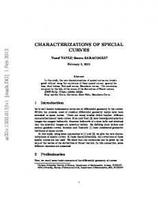
4.7 g/cm3 , respectively. According to EDS results in Table 1, Ti, Ti-20Ta, Ti-10Ta, and Ti-10Mo formed 100% TiO2 , 83.9% TiO2 + 16.1% Ta2 O5 , 91.3% TiO2 + 8.7% Ta2 O5 , and 92.8% TiO2 + 7.2% MoO3 . The densities of 100% TiO2 , 83.9% TiO2 + 16.1% Ta2 O5 , 91.3% TiO2 + 8.7% Ta2 O5 , and 92.8% TiO2 + 7.2% MoO3 were 4.23 g/cm3 , 4.84 g/cm3 , 4.54 g/cm3 , and 4.24 g/cm3 , respectively. Therefore, the mass of nanotubes films 1 cm2 sample for each alloy was listed in Table 2 being 5.32 mg/cm2 , 6.09 mg/cm2 , 5.72 mg/cm2 , and 5.34 mg/cm2 . Cyclic voltammograms (CV) are used to characterize the capacitors behavior of the alloy oxide nanotubes. Figure 9 shows capacitance performance evaluations for the Ti alloy anodic oxide nanotubes by cyclic voltammograms. It is clear that Ti alloy oxide nanotubes had larger area of CV curve than pure TiO2 nanotube did. It means that Ti alloys oxide nanotubes had larger capacitances than pure TiO2 nanotubes. Besides, more Ta2 O5 content can significantly enhance the capacitor performance by comparing two Ti-Ta alloys curves with different compositions. Moreover, Ti-10Mo alloy oxide nanotubes CV curve shows a symmetrical shape which indicates that the revisable redox reaction of Mo2+ /Mo3+ was helpful to improve the capacitor performance. The specific capacitance (𝐶) can be measured by voltage step, current step, or voltage ramp methods and evaluated by the equations of 𝐶 = 𝑄/𝑉 and 𝐶 = 𝑑𝑄/𝑑𝑉 [35], where 𝑉 is applied voltage and 𝑄 is the quantity of charge on the electrode (which can be evaluated from the area of the CV curve). Table 2 shows the specific capacitance based on 1 cm2 sample area and 20 𝜇m film thickness of pure Ti, Ti-20Ta, Ti-10Ta, and Ti-10Mo oxide nanotubes films which are 13.7 F/g, 26.1 F/g, 23.3 F/g, and 21.4 F/g, respectively. The specific capacitances of Ti alloys oxide nanotubes films were higher than that of TiO2 -B nanowires/MWCNTs hybrid supercapacitor with specific capacitance of 17.7 F/g [36].
4. Conclusions In summary, we fabricated ultracapacitors based on the working electrode made of highly ordered anodic TiO2 , Ta2 O5 , and MoO3 nanotubes directly formed on pure Ti, Ti-20Ta, Ti-10Ta, and Ti-10Mo substrates. The ordered alloys oxide nanotubes structure has a volume of 1.26 × 10⁻³ cm3 in 1 cm2 sample area with nanotube density of 4.5 × 10⁹ tubes/cm2 . The mass of pure Ti and Ti alloys oxide nanotubes films with 1 cm2 sample size and 20 𝜇m film thickness can be calculated as 5.32 mg (TiO2 nanotubes), 6.09 mg (Ti-20Ta oxide nanotubes), 5.72 mg (Ti-10Ta oxide nanotubes), and 5.34 mg
8
Journal of Nanomaterials 4
R3
TiO2 -20Ta2 O5 Current density (mA/cm2 )
Top R1 R1 T1 H
Ti-10MoO3
2 0
TiO2
−2 −4 −6 −1.1
−0.8
R2 R2
T2 W
Outer surface
H+W
Inner surface 2𝜋R2
Acknowledgment
(c)
This study was partially supported by a Grant from the National Science Council, Taiwan (102-3113-P-042A-005-).
(d)
Figure 7: Estimation of TiO2 NT surface: (a) cone structure of inner tube with radius of 𝑅3 , and 𝑅1 , and 𝑅2 on the tube top and bottom, tube length with 𝐻, (b) pore wall thickness with 𝑇1 and 𝑇2 on the tube top and bottom, (c) tube inner surface area, and (d) outer surface area. 2500
Surface area (cm2 )
2000 Outer surface area 1500 1000 500
Inner surface area 0
0.1
(Ti-10Mo oxide nanotubes), respectively. Furthermore, Ti alloy anodic oxide nanotubes films with 1 cm2 surface and 20 𝜇m thickness have an inner surface area of 241.0 cm2 and outer surface area of 480.4 cm2 . Thus, such large surface area of dielectric oxides caused very high specific capacitances. The specific capacitance can further be enhanced by (1) reacting with barium nitrate (Ba(NO3 )2 ) [37] or barium hydroxide (Ba(OH)2 ) [38] to form a very high dielectric constant BaTiO3 film, (2) increasing nanotubes length by longer anodization process, and (3) increasing nanotubes surface area by coating TiO2 nanoparticles on the nanotubes surface [39].
4√3(R1 + T1 )
0
−0.2
(b)
2𝜋R1
L
−0.5 SEC (V)
Figure 9: Capacitance performance evaluations for TiO2 NT, TiO2 10 Ta2 O5 NT, TiO2 -20 Ta2 O5 NT, and TiO2 -10 MoO3 NT by cyclic voltammograms.
Bottom
(a)
TiO2 -10Ta2 O5
25
50
75
100
Length (𝜇m)
Figure 8: Accumulated anodic Ti and Ti alloy NT inner and outer surface areas based on 1 cm2 substrate.
References [1] L. E. Cross, “Ferroelectric materials for electromechanical transducer applications,” Materials Chemistry and Physics, vol. 43, no. 2, pp. 108–115, 1996. [2] A. D. Hilton and R. Frost, “Recent developments in the manufacture of barium titanate powders,” Key Engineering Materials, vol. 66, pp. 145–184, 1992. [3] L. E. Cross, “Dielectric, piezoelectric and ferroelectric components,” American Ceramic Society Bulletin, vol. 63, no. 4, pp. 586–590, 1984. [4] D. Pandey, A. P. Singh, and V. S. Tiwari, “Developments in ferroelectric ceramics for capacitor applications,” Bulletin of Materials Science, vol. 15, no. 5, pp. 391–402, 1992. [5] K. Kajiyoshi, N. Ishizawa, and M. Yoshimura, “Preparation of tetragonal barium titanate thin film on titanium metal substrate by hydrothermal method,” Journal of the American Ceramic Society, vol. 74, no. 2, pp. 369–374, 1991. [6] T. Horikawa, N. Mikami, T. Makita et al., “Dielectric properties of (Ba, Sr)TiO3 thin films deposited by RF sputtering,” Japanese Journal of Applied Physics, vol. 32, no. 9, pp. 4126–4130, 1993.
Journal of Nanomaterials [7] A. S. Shaikh and G. M. Vest, “Kinetics of BaTiO3 and PbTiO3 formation from metallo-organic precursors,” Journal of the American Ceramic Society, vol. 69, no. 9, pp. 682–688, 1986. [8] H. Okamura and H. K. Bowen, “Preparation of alkoxides for the synthesis of ceramics,” Ceramics International, vol. 12, no. 3, pp. 161–171, 1986. [9] K. W. Kirby, “Alkoxide synthesis techniques for BaTiO3 ,” Materials Research Bulletin, vol. 23, no. 6, pp. 881–890, 1988. [10] P. Bhattacharya, T. Komeda, K.-H. Park, and Y. Nishioka, “Comparative study of amorphous and crystalline (Ba, Sr)TiO3 thin films deposited by laser ablation,” Japanese Journal of Applied Physics, vol. 32, no. 9, pp. 4103–4106, 1993. [11] D. M. Tahan, A. Safari, and L. C. Klein, “Preparation and characterization of Ba𝑥 Sr1−𝑥 TiO3 thin films by a Sol-Gel technique,” Journal of the American Ceramic Society, vol. 79, no. 6, pp. 1593– 1598, 1996. [12] C.-C. Chen, J.-H. Chen, C.-G. Chao, and W. C. Say, “Electrochemical characteristics of surface of titanium formed by electrolytic polishing and anodizing,” Journal of Materials Science, vol. 40, no. 15, pp. 4053–4059, 2005. [13] C.-C. Chen, Y. Bisrat, Z. P. Luo, R. E. Schaak, C.-G. Chao, and D. C. Lagoudas, “Fabrication of single-crystal tin nanowires by hydraulic pressure injection,” Nanotechnology, vol. 17, no. 2, pp. 367–374, 2006. [14] H. Tsuchiya and P. Schmuki, “Self-organized high aspect ratio porous hafnium oxide prepared by electrochemical anodization,” Electrochemistry Communications, vol. 7, no. 1, pp. 49–52, 2005. [15] I. Sieber, H. Hildebrand, A. Friedrich, and P. Schmuki, “Formation of self-organized niobium porous oxide on niobium,” Electrochemistry Communications, vol. 7, no. 1, pp. 97–100, 2005. [16] I. Sieber, B. Kannan, and P. Schmuki, “Self-assembled porous tantalum oxide prepared in H2 SO4 /HF electrolytes,” Electrochemical and Solid-State Letters, vol. 8, no. 3, pp. J10–J12, 2005. [17] N. Mukherjee, M. Paulose, O. K. Varghese, G. K. Mor, and C. A. Grimes, “Fabrication of nanoporous tungsten oxide by galvanostatic anodization,” Journal of Materials Research, vol. 18, no. 10, pp. 2296–2299, 2003. [18] G. B. Stefanovich, A. L. Pergament, A. A. Velichko, and L. A. Stefanovich, “Anodic oxidation of vanadium and properties of vanadium oxide films,” Journal of Physics: Condensed Matter, vol. 16, no. 23, pp. 4013–4024, 2004. [19] N. K. Shrestha, Y.-C. Nah, H. Tsuchiya, and P. Schmuki, “Self-organized nano-tubes of TiO2 -MoO3 with enhanced electrochromic properties,” Chemical Communications, no. 15, pp. 2008–2010, 2009. [20] I. Paramasivam, Y.-C. Nah, C. Das, N. K. Shrestha, and P. Schmuki, “WO3 /TiO2 nanotubes with strongly enhanced photocatalytic activity,” Chemistry—A European Journal, vol. 16, no. 30, pp. 8993–8997, 2010. [21] A. Ghicov, S. Aldabergenova, H. Tsuchyia, and P. Schmuki, “TiO2 -Nb2 O5 nanotubes with electrochemically tunable morphologies,” Angewandte Chemie—International Edition, vol. 45, no. 42, pp. 6993–6996, 2006. [22] Y. Yang, D. Kim, M. Yang, and P. Schmuki, “Vertically aligned mixed V2 O5 -TiO2 nanotube arrays for supercapacitor applications,” Chemical Communications, vol. 47, no. 27, pp. 7746–7748, 2011. [23] H. Jha, R. Hahn, and P. Schmuki, “Ultrafast oxide nanotube formation on TiNb, TiZr and TiTa alloys by rapid breakdown anodization,” Electrochimica Acta, vol. 55, no. 28, pp. 8883–8887, 2010.
9 [24] W. Wei, S. Berger, N. Shrestha, and P. Schmuki, “Ideal hexagonal order: formation of self-organized anodic oxide nanotubes and nanopores on a Ti-35Ta alloy,” Journal of the Electrochemical Society, vol. 157, no. 12, pp. C409–C413, 2010. [25] H. Tsuchiya, S. Berger, J. M. Macak, A. Ghicov, and P. Schmuki, “Self-organized porous and tubular oxide layers on TiAl alloys,” Electrochemistry Communications, vol. 9, no. 9, pp. 2397–2402, 2007. [26] R. J. D. Tilley, “Correlation between dielectric constant and defect structure of non-stoichiometric solids,” Nature, vol. 269, no. 5625, pp. 229–231, 1977. [27] J. Lin, N. Masaaki, A. Tsukune, and M. Yamada, “Ta2 O5 thin films with exceptionally high dielectric constant,” Applied Physics Letters, vol. 74, no. 16, pp. 2370–2372, 1999. [28] H. Segawa, K. Mori, M. Itagati, K. Sakurki, and T. Ishiwta, “Image sensing device,” US patent no. 4499384, 1985. [29] C. C. Chen, D. Fang, and Z. Luo, “Fabrication and characterization of highly-ordered valve-metal oxide nanotubes and their derivative nanostructures,” Reviews in Nanoscience and Nanotechnology, vol. 1, no. 4, pp. 1–28, 2012. [30] M. Pourbaix, Atlas of Electrochemical Equilibria in Aqueous Solutions, NACE, Houston, Tex, USA, 1974. [31] C. W. Lai and S. Sreekantan, “Effect of applied potential on the formation of self-organized TiO2 nanotube arrays and its photoelectrochemical response,” Journal of Nanomaterials, vol. 2011, Article ID 142463, 7 pages, 2011. [32] J. H. Lim and J. Choi, “Titanium oxide nanowires originating from anodically grown nanotubes: the bamboo-splitting model,” Small, vol. 3, no. 9, pp. 1504–1507, 2007. [33] J. Tao, J. Zhao, X. Wang, Y. Kang, and Y. Li, “Fabrication of titania nanotube arrays on curved surface,” Electrochemistry Communications, vol. 10, no. 8, pp. 1161–1163, 2008. [34] D. Kim, F. Schmidt-Stein, R. Hahn, and P. Schmuki, “Gravity assisted growth of self-organized anodic oxide nanotubes on titanium,” Electrochemistry Communications, vol. 10, no. 7, pp. 1082–1086, 2008. [35] A. J. Bard and L. R. Faulkner, Electrochemical Methods, Fundamentals and Applications, John Wiley & Sons, Singapore, 1980. [36] G. Wang, Z. Y. Liu, J. N. Wu, and Q. Lu, “Preparation and electrochemical capacitance behavior of TiO2 -B nanotubes for hybrid supercapacitor,” Materials Letters, vol. 71, pp. 120–122, 2012. [37] L. Zhang, Y. Shi, S. Peng, J. Liang, Z. Tao, and J. Chen, “Dyesensitized solar cells made from BaTiO3 -coated TiO2 nanoporous electrodes,” Journal of Photochemistry and Photobiology A, vol. 197, no. 2-3, pp. 260–265, 2008. [38] X. Wei, “Hydrothermal synthesis of BaTiO3 thin films on nanoporous TiO2 covered Ti substrates,” Journal of Crystal Growth, vol. 286, no. 2, pp. 371–375, 2006. [39] C.-C. Chen, H.-W. Chung, C.-H. Chen et al., “Fabrication and characterization of anodic titanium oxide nanotube arrays of controlled length for highly efficient dye-sensitized solar cells,” Journal of Physical Chemistry C, vol. 112, no. 48, pp. 19151–19157, 2008.
Journal of
Nanotechnology Hindawi Publishing Corporation http://www.hindawi.com
Volume 2014
International Journal of
International Journal of
Corrosion Hindawi Publishing Corporation http://www.hindawi.com
Polymer Science Volume 2014
Hindawi Publishing Corporation http://www.hindawi.com
Volume 2014
Smart Materials Research Hindawi Publishing Corporation http://www.hindawi.com
Journal of
Composites Volume 2014
Hindawi Publishing Corporation http://www.hindawi.com
Volume 2014
Journal of
Metallurgy
BioMed Research International Hindawi Publishing Corporation http://www.hindawi.com
Volume 2014
Nanomaterials
Hindawi Publishing Corporation http://www.hindawi.com
Volume 2014
Submit your manuscripts at http://www.hindawi.com Journal of
Materials Hindawi Publishing Corporation http://www.hindawi.com
Volume 2014
Journal of
Nanoparticles Hindawi Publishing Corporation http://www.hindawi.com
Volume 2014
Nanomaterials Journal of
Advances in
Materials Science and Engineering Hindawi Publishing Corporation http://www.hindawi.com
Volume 2014
Journal of
Hindawi Publishing Corporation http://www.hindawi.com
Volume 2014
Journal of
Nanoscience Hindawi Publishing Corporation http://www.hindawi.com
Scientifica
Hindawi Publishing Corporation http://www.hindawi.com
Volume 2014
Journal of
Coatings Volume 2014
Hindawi Publishing Corporation http://www.hindawi.com
Crystallography Volume 2014
Hindawi Publishing Corporation http://www.hindawi.com
Volume 2014
The Scientific World Journal Hindawi Publishing Corporation http://www.hindawi.com
Volume 2014
Hindawi Publishing Corporation http://www.hindawi.com
Volume 2014
Journal of
Journal of
Textiles
Ceramics Hindawi Publishing Corporation http://www.hindawi.com
International Journal of
Biomaterials
Volume 2014
Hindawi Publishing Corporation http://www.hindawi.com
Volume 2014