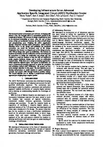
the standard cell design implements the digital control and non-time critical .... identical programmable delay generators to produce the two independent clocks.
TTCrx, AN ASIC FOR TIMING, TRIGGER AND CONTROL DISTRIBUTION IN LHC EXPERIMENTS J. Christiansen, A. Marchioro and P. Moreira, CERN - ECP/MIC, Geneva, Switzerland ABSTRACT An ASIC receiver was developed for the LHC Timing, Trigger and Control (TTC) distribution system. The ASIC implements an interface between the front–end electronics and the TTC system making the TTC coding and multiplexing schemes transparent to the users. The receiver delivers the LHC timing reference signal, the first level trigger decisions and its associated bunch and event numbers. It can be programmed to compensate for the propagation delays associated with the detectors and their electronics. The IC supports the transmission of data and of synchronised broadcast commands. The ASIC was implemented in a standard 1 µm CMOS process using a combination of full custom and standard cell design techniques. The jitter measured on the recovered clock is less than 80 ps RMS for input optical powers down to -22 dBm. The time deskewing functions allows the commands and the first level trigger accept signal to be phase shifted up to a maximum of sixteen clock cycles in steps of 0.1 ns with an RMS error of 92 ps.
purposes of internal and external control. Bunch crossing and event identification numbers are also made available. Figure 1 shows the architecture chosen to implement this functionality. In this figure the broken line represents the boundary between the full custom and the standard cell part of the design. The full custom part implements all the analogue and timing critical functions of the receiver, while the standard cell design implements the digital control and non-time critical functions. Clock Extraction Input from PINFET
A passive optical fibre network has been proposed to distribute the LHC Timing, Trigger and Control (TTC) information to several thousand front-end electronic destinations using a single laser source [1,2]. At the transmitter end, two communication channels are time division multiplexed and coded in the BiPhase Mark (BPM) format, before they are optically transmitted over the network. One of the multiplexed channels carries the firstlevel trigger-accept signal while the other is used to transmit general broadcast and individually addressed commands. A timing receiver is associated to each of the outputs of the optical network. This receiver is composed of a commercial integrated photodetector-preamplifier and the special purpose IC (TTCrx) described in this paper [3]. The TTCrx ASIC receives the information broadcast over the TTC distribution network and makes it available to electronics both inside and outside the LHC detectors.
2. TTCrx ARCHITECTURE The main functions of the timing receiver are to recover the 40.08 MHz LHC reference clock with minimum jitter, to distribute the first-level trigger-accept decisions and broadcast commands and to make them available to the detector electronics properly deskewed in time. Additionally, the receiver recognises individually addressed commands for
CLK φ1 CLK φ2
4φ
Data Decoder/ Demultiplexer Full Custom
A
B
Standard Cells Local Address
Internal Registers and
JTAG
1. INTRODUCTION
Linear Receiver
Programmable Fine Deskews
Control
A-B Channels Identification
Control & Data Interface
Error Monitoring
Bunch/Event Counters
Serial/Parallel Converter
Coarse Deskew Functions
L1 Accept Bunch No/ Event No Bcast CMDS/ Sub-address Data Error
Figure 1 Timing receiver chip block diagram As shown in Figure 1, the ASIC receives the TTC data in the form of an electrical signal from the optical preamplifier. Due to the optical power levels detected by the preamplifier, this signal needs to be amplified to CMOS levels before it can be used for clock recovery, data decoding and demultiplexing. The unit marked as “Linear Receiver” in Figure 1 implements that function. Signal level detection and automatic gain control are also taken care of inside this block. After the signal is restored to CMOS levels, it is fed to the “Clock Extraction” and the “Data Decoder/ Demultiplexer” units where the LHC system clock is recovered with minimum jitter, and the trigger (A) and data (B) channels are separated. The recovered clock is then fed to the “Programmable Fine Deskew” unit where two different clock phases, synchronous with the LHC system clock, are generated. The phases of the two clocks can be controlled independently via commands on the B channel. The “Programmable Fine Deskew” unit allows the two clock phases to be changed in steps of 104 ps between 0 and 25 ns. The TTCrx control logic consists of three major blocks. The first block contains the internal configuration and status registers and implements the logic necessary to read a 14 bit number from an external serial configuration PROM that supplies the TTCrx ASIC with its unique system address. The
logic in this block also implements a functional subset of the JTAG/IEEE 1149.1 standard [4] providing the capability for the ASIC to be used in board-level connectivity tests. The second block identifies the trigger and data channels and constantly monitors the data in channel B for transmission errors. It deserializes the received data and decides if these are addressed to the IC itself or to some external addressable or common space. Finally, the third functional block implements two independently programmed coarse deskewing functions for the first-level trigger signal and the broadcast commands. The related control registers can be programmed by individually addressed data transmitted over the B channel. Both first-level trigger and broadcast commands can be deskewed over a range of 16 bunchcrossing intervals.
processing of the signal or a locking acquisition aid mechanism. Typically, circuits designed to recover the clock from a BPM signal require an external quartz oscillator to serve as a timing reference in the initial phase of the lock acquisition process. However, for the application in question, it was undesirable to adopt such a solution. To solve the lock acquisition problem, a strategy was adopted where the signal out of the discriminator is first fed to a sequential circuit that generates a reference clock signal from the BPM encoded data. This signal is then filtered by a narrow bandwidth Phase Locked Loop (PLL) that generates the desired low jitter reference clock. A simplified diagram of the clock reference generator circuit is shown in Figure 3. A) in a out
tp
2.1 The Linear Receiver
tp
The signal received by the optical receiver preamplifier is amplified and converted to CMOS levels by the “Linear Receiver” unit whose block diagram is given in Figure 2.
Q
R
Delay Locked Loop
ts Q
S
DLL control voltage
Gain Controlled Amplifier
Discriminator
Bin
�
DT
A
Peak Detector
a
Ref.
out
Figure 2 TTCrx “Linear Receiver” unit block diagram As shown in the above diagram, the linear part of the TTCrx is composed of a Gain Controlled Amplifier (GCA), a peak detector, a loop amplifier, a loop filter (integrator) and a discriminator. The signal path in this design is fully differential with the conversion to single ended taking place only in the last stage of the discriminator. To achieve a gain bandwidth product compatible with the system requirements, using the relatively slow 1µm CMOS process, the gain controlled amplifier was designed as a cascade of six identical gain stages. The design is similar to that reported in [5], but with the triode voltage controlled resistors replaced by linearised floating resistors [6]. The output of the gain controlled amplifier is converted to CMOS logic levels by the discriminator. A moderate amount of positive feedback is used in this circuit to achieve fast operation while at the same time avoiding undesirable hysteresis effects [7]. Finally, since the expected optical signal power variations are mainly due to fibre darkening under radiation and to the laser transmitter ageing, the gain control loop was designed with a long time constant.
2.2 Clock and Data Extraction Since the biphase mark coding scheme is characterised by constant phase inversions, it is not possible to recover the clock directly from the data without some kind of pre-
R
S
Q
ts
Figure 3 A) Clock reference generator circuit B) Timing diagram In this circuit, at the output of the XOR gate (point a in Figure 3), rectangular pulses are generated at each transition of the input signal. The sequential circuit, composed of the AND gate, the RS flip-flop and the time delays tp and ts, suppresses the pulses generated by the half bit interval transitions of the BPM encoded data. In this way, at the output, a periodic signal of twice the LHC clock frequency is generated. After division by two, this signal is used as time reference by the narrow band PLL as illustrated in Figure 4. Note that, after initialisation, the reference signal always aligns with the data bit boundaries once the first data zero is 1 detected . The correct operation of this circuit depends strongly on the circuit’s ability to correctly set the time delay ts. The precision required is superior to what can be expected from process parameters and temperature variations. To overcome this problem, a Delay Locked Loop (DLL) is used
1
The initialisation circuit has been omitted from the figure for simplicity.
to regulate the delay ts. A special Phase Detector (PD) was designed which allows the DLL to lock directly on the BPM encoded data. When the delay ts is built and controlled in the same way as the delay chain in the DLL, it is possible to obtain a good precision in t s. Clock Reference Generator
clock signal but this time ∆ t(N-1) = T/(N-1) seconds apart. By appropriate output tap selection in each DLL the clock signal can be shifted with a time resolution that is given by: ∆ t = ∆ t(N-1) - ∆ tN N in
Phase Detector and
D U/D Charge Pump (1)
Loop Filter
P VCO I
R
U
V
D
Φ4 Φ3 Φ2 Φ1 Φ0
MUX
sel
Charge Pump (2)
N-1 Phase Detector and
. Figure 4 Phase and Frequency Locked Loop block diagram The Phase Frequency Locked Loop (PFLL) represented in Figure 4 uses separate frequency and phase detectors in the control loop. The loop is designed in such a way that the frequency detector dominates the PFLL behaviour when far away from lock. In this case, the PFLL has a frequency sensitive operation. When in lock, the loop behaviour is dictated by the phase detector alone. Since this last has a better phase resolution than the frequency detector, it is possible to obtain a frequency sensitive PLL while, at the same time, maintaining good phase resolution. This minimises the jitter of the recovered clock while keeping the loop operation tolerant to process and temperature variations without the need for external trimming components. The PFLL uses a three state phase detector [8] for frequency acquisition and a D flip-flop type PD [9,10] for phase acquisition and tracking. Data decoding and demultiplexing of the trigger and data channels are made inside the “Data Decoder/Demultiplexer” unit using the four-phase clock signals generated in the clock recovery circuit.
2.3 Fine Clock Deskewing Function The recovered clock is fed to the “Programmable Fine Deskew” unit. There, two independently controlled clock signals are generated and made externally available. The two clock signals are controlled using data transmitted over the TTC distribution system. They can be programmed in steps of 104 ps up to a maximum delay corresponding to a bunch crossing interval. The “Programmable Fine Deskew” unit contains two identical programmable delay generators to produce the two independent clocks. In order to obtain a sub-gate delay resolution a novel architecture based on two staggered delay locked loops was used. Its principle of operation can be easily understood with reference to Figure 5. In this scheme, the first DLL generates N replicas of the recovered clock each one of them delayed by ∆ tN = T/N seconds from the previous one, where T is the recovered clock period. One of these signals is selected as the input to the following delay locked loop. The second DLL generates N-1 copies of the
Loop Filter
MUX
sel
out
. Figure 5 Programmable sub-gate resolution delay generator In the present case, N=16 was used, resulting in a minimum combined time step of 104.0 ps The scheme presented here has the advantages of providing well defined time steps and of being self calibrating since it uses the LHC recovered system clock as the timing reference. The circuit and operation details of the DLL used to implement the programmable delay generators have been previously described in [10].
2.4. Digital Control Logic Functionality Each TTCrx IC is identified in the distribution network by a unique 14-bit channel Identification (ID) number. This number is read from the serial PROM at power up or after a reload ID broadcast command is received. The ASIC control logic identifies the A and B channels, deserializes the data in the B channel and continuously monitors it to look for the presence of its ID channel number. Data in channel B can be of two types [1,2]: Broadcast commands and individually addressed data/commands. Broadcast commands are used to distribute messages to all TTC receivers in the system. When detected, these commands are executed by all the timing ASICs. These messages are also made available to the outside electronics. The individually addressed data/commands are implemented in the TTC system to transmit user-defined data and commands over the network. These commands have two distinct modes of operation. In the first mode, they are aimed at the TTC receivers themselves and their user-defined content is used to control the receiver’s operation. In the second mode, the data are intended for the external electronics. In this case, both the data and sub-address contents of the received commands are made externally available. Both the broadcast and the individually addressed commands are transmitted over the TTC network using a frame format
ignored and the contents of the Double Bit/Frame Error register incremented. The contents of the internal error counters are dumped on the external data bus when an error dump broadcast command is issued by the central TTC system.
3. MEASUREMENTS In this section we present the measurement results for the clock recovering and fine deskewing functions. Measurement results concerning the analogue functions of the IC have already been reported in a previous publication [12].
3.1 Clock Recovering and Fine Deskew Function The IC was connected to a 11 KΩ photodetector-preamplifier and the jitter of the recovered clock measured. The input optical signal was a biphase mark encoded PRBS provided by the TTC transmitter. Figure 6 shows the measurement results for the recovered clock jitter at the output of the reference generator circuit (doted line), at the output of the PLL (solid line) and at the output of the programmable delay generator (dashed line). TTCrx Jitter 350
300
Ref. Gen. PLL DLL
250 Measured rms jitter (ps)
that has been specified in reference [3]. The frame structure contains several fields to control the transmission and includes a field in which several redundant bits are inserted for error detection and correction. The coding scheme used is a standard Hamming code with the capability of double error detection and single bit error correction. Error detection and correction is implemented for both the broadcast and the individually addressed commands. The TTCrx contains several internal registers used for control and monitoring of its operation. These registers are: The Configuration register, Control register, Coarse Delay register, Fine Delay registers, Bunch Counter register, Event Counter register, Single Bit Error Counter and Double Bit/Frame Error counter. The Configuration register contains the configuration bits read during initialisation from the external serial PROM. It is used to store the 14-bit chip ID and to set up some of the different ASIC operation and test modes. The Control register is used to minimise the IC power consumption by allowing the disabling of some of the chip functionality in applications that do not require it. For instance, the Event and Bunch counters and the Address and Data buses can be disabled if not required by the external electronics. The Coarse Delay register holds the deskewing parameters for the First Level Trigger Accept (L1A) and the Bunch Counter Reset signals. The contents of this register in conjunction with that of the Fine Delay register affects the total amount of deskewing. Since the same deskewing is applied to the L1A signal and the broadcast commands, deskewing of the latter ones will also have to be performed at the source of the TTC system to compensate for the time necessary to transmit and decode these commands. The Fine Delay registers hold the deskewing parameters that control the programmable delay generator discussed previously. When combined with the coarse deskewing functions, a compensation range of 16 bunch-crossing intervals is obtained. This allows a substantial margin beyond the possible maximum variations due to differences in timeof-flight and optical fibre path lengths in the detectors. The Bunch Counter and the Event Counter registers are free running counters that are incremented by the recovered clock and the L1A signals, respectively. These counters can be reset by specially defined broadcast commands. The Bunch Counter register content, which is a 12-bit number, is normally available to the outside logic. However, during the two clock cycles following a trigger accept, the 24-bit Event Number register content can optionally be made available to the outside electronics on the same 12 output lines. Finally, the Single Bit Error and the Double Bit/Frame Error counters are used to keep track of the number of errors occurring during data reception. Since the receiver Hamming decoder is capable of fully recovering from single bit errors, the data are accepted after correction and the Single Bit Error register incremented. When a double bit error is recognised by the receiver logic or a frame error is detected, the data are
200
150
100
50
0 −22
−20
−18 −16 −14 Input optical power (dBm)
−12
−10
Figure 6 Measured RMS jitter From this figure it can be seen that the jitter of the recovered clock is always less than 80 ps RMS over the whole operation range. This figure also shows that the programmable delay generator is not introducing any significant amount of jitter and that the PFLL is effectively filtering the jitter of the signal generated by the reference generator circuit. The linearity of the of the delay generator was also measured and the results are shown in Figure 7 and Figure 8. The delay generator allows the clock phase to be shifted in steps of 0.1 ns up to a maximum of 25 ns with an RMS error of 92 ps. It is, however, necessary to mention that the linearity of the programmable delay generator is strongly influenced by the
presence of parasitic package inductance. The results reported here were obtained with the IC directly bonded to the PCB to minimise inductance. For a common package (PGA 100) the RMS error degrades to 200 ps. Different packaging solutions for the TTCrx are now being studied in order to minimise this effect.
time. Additionally, the receiver allows broadcast and addressed commands to be transmitted over the network. The measurement results show that it is possible to recover the LHC clock from the TTC multiplexed and encoded data with an RMS jitter better than 80 ps and to control its phase in steps of 0.1 ns with an RMS error smaller than 100 ps.
Measured delay (ns)
PCB bonded chip 25
5. ACKNOWLEDGEMENTS
20
The authors wish to acknowledge Bruce G. Taylor for valuable discussions on this work and Ernst Murer for the preparation of the test set-up and for helping with the measurements.
15
REFERENCES 10
5
0 0
5
10 15 Programmed delay (ns)
20
25
Figure 7 Measured delay as function of the programmed delay PCB bonded chip 60
50 RMS = 0.0915ns 40
PP = 0.4885ns
30
20
10
0
−0.6
−0.4
−0.2 0 0.2 Measured delay error (ns)
0.4
0.6
Figure 8 Delay error histogram
4. CONCLUSION An ASIC receiver to be used with the LHC Timing, Trigger and Control distribution system was designed, fabricated and tested. The receiver is intended to recover the LHC reference clock and to distribute it together with first level trigger decisions to the detector electronics properly deskewed in
[1] B. G. Taylor, “Timing, Trigger and Control (TTC) Systems for LHC Detectors,” CERN/ECP http://www.cern.ch/TTC/ intro.html. [2] B. G. Taylor, “TTC Distribution,” Proceedings of the First Workshop on Electronics for LHC Experiments, Lisbon, 11-15 September 1995, (CERN/LHCC/95-56), pp. 180-184. [3] J. Christiansen, A. Marchioro and P. Moreira, “TTCrx Reference Manual — A Timing, Trigger and Control Distribution Receiver ASIC for LHC Detectors,” CERN/RD12 working document. [4] C. M. Maunder and R. E. Tulloss, “The Test Access Port and Boundary-Scan Architecture,” IEEE Computer Society Press, 1990 [5] T. H. Hu and P. R. Gray, “A Monolithic 480 Mb/s Parallel AGC/Decision/Clock-Recovery Circuit in 1.2µm CMOS,” J. Solid-State Circuits, vol. SC-28, pp. 1314-1320, December 1993. [6] M. Banu and Y. Tsividis, “Floating Voltage-Controlled Resistors in CMOS Technology,” Electronics Letters, vol. 18, pp. 678-679, July 1982. [7] D. J. Allstot, “A Precision Variable-Supply CMOS Comparator”, J. Solid-State Circuits, vol. SC-17, pp. 1080-1079, December 1982. [9] M. Soyuer and R. Meyer, “Frequency Limitations of a Conventional Phase-Frequency Detector,” J. Solid-State Circuits, vol. SC-25, pp. 1019-1022, August 1990. [10]M. Johnson and E. Hudson, “A Variable Delay Line for CPU Co-Processor Synchronization,” J. Solid-State Circuits, vol. SC-23, pp. 1218-1223, October 1988. [11]J. Christiansen, “An Integrated CMOS 0.15ns Digital Timing Generator for TDC’s and Clock Distribution Systems,” IEEE Trans. Nuclear Science, vol. 42, pp. 753-757, August 1995. [12]J. Christiansen, A. Marchioro, P. Moreira, and A. Sancho, “Receiver ASIC for Timing, Trigger and Control Distribution in LHC Experiments,” Trans. Nuclear Science, vol. 43, pp. 1773 –1777, June 1996.