VHDL-Based Design and Design Methodology for Reusable High Performance Direct Digital Frequency Synthesizers* Ireneusz Janiszewski1
Bernhard Hoppe
Hermann Meuth
FH Darmstadt Fachbereich Elektrotechnik Schöfferstr. 3, D-64295 Darmstadt +49-6151-168268
FH Darmstadt Fachbereich Elektrotechnik Schöfferstr. 3, D-64295 Darmstadt +49-6151-168322
FH Darmstadt Fachbereich Elektrotechnik Schöfferstr. 3, D-64295 Darmstadt +49-6151-168322
[email protected]
[email protected]
[email protected]
ABSTRACT Design methodologies for high performance Direct Digital Frequency Synthesizers (DDFS) are described. Traditional look-up tables (LUT) for sine and cosine are merged with CORDIC-interpolation into a hybrid architecture. This implements DDFS-systems with high resolution without being specific to a particular target technology. Amplitude constants were obtained from mathematical trigonometric functions of the IEEE math_real package. These constants were then written via simulation of a VHDL model into a fully synthesizable package. Systematic and detailed studies varying the synthesizer’s inherent parameters lead to a design optimum of the LUT/CORDIC-ratio, which minimizes power and silicon area for a given clock frequency.
Categories and Subject Descriptors M1.5: Logic and high-level synthesis and optimization
General Terms Algorithms, Design, Languages, Theory.
Keywords HDL-based Design, Direct Frequency Synthesis, Design Optimization and Reuse, CORDIC Algorithm.
1. INTRODUCTION Direct Digital Frequency Synthesis (DDFS) based on Numerically Controlled Oscillators (NCO) is an established method for generating quasi-periodic sinusoid signals whenever high frequency resolution, fast changes in frequency and phase, and high spectral purity of the output signal are required [1]. Applications range from instrumentation to modern communication systems, including spread-spectrum and phase shift-keying modulation techniques [2,3]. The paper presents a design methodology for highPermission to make digital or hard copies of all or part of this work for personal or classroom use is granted without fee provided that copies are not made or distributed for profit or commercial advantage and that copies bear this notice and the full citation on the first page. To copy otherwise, or republish, to post on servers or to redistribute to lists, requires prior specific permission and/or a fee. DAC 2001, June 18-22, 2001, Las Vegas, Nevada, USA Copyright 2001 ACM 1-58113-297-2/01/0006…$5.00.
performance high-precision reusable DDFS cells suitable for unrestricted porting into any available semiconductor technology and, as a functional block, into any system-on-a-chip design, containing an NCO. The innovative aspects of our approach are •
the technology independent HDL-description of the design;
•
part of the design files needed for synthesis is generated via simulation of a VHDL model, as mathematical functions from math_real package are not directly synthesizable;
•
a new efficient hybrid generation scheme for the signal amplitudes, combining within the same model look-up tables (LUTs) with CORDIC algorithmic procedures.
No technology specific ROM generators have to be employed. If LUT and CORDIC portions are properly balanced, the sine and cosine amplitudes may be obtained by means of efficient combinatorial implementations of the LUTs by logic gates, especially for high phase and frequency resolution. This hybrid scheme combines the advantages of both the LUT and CORDIC approach: (i) fast access and power efficiency of moderately-sized LUTs and (ii) arbitrary precision obtainable from a systematic iteration algorithm. The design portfolio obtained by moving from full CORDIC- to LUT-architectures was completely explored by systematic case studies using VHDL models, simulation and synthesis. These experiments show, that optimum LUT/CORDIC ratios can minimize use of power and silicon area for a given maximum clock frequency. The hybrid scheme is compatible with a synthesis based standard semi-custom design flow to arbitrary target technologies, and, hence, constitutes a truly reusable implementation. Pure ROM-based direct digital frequency synthesizers, in contrast, typically resort to a full-custom flow for the LUTs. As in many high performance design problems the performance is intimately related to the cost of hardware implementation. In order to critically examine this tradeoff we developed a methodology which allows for evaluating actual hardware costs by means of synthesis to and layout generation in a particular technology. For this end a single model approach was developed, containing the complete design, permitting parametric variation of the set of design parameters. *This work was supported by the German Federal Ministry of Education and Research under contract FKZ1709399.
xi+1 = xi - σi yi 2-i
2. DIGITAL FREQUENCY SYNTHESIS An NCO is a digital block, which renders digital word sequences in time at a given clock frequency fCLK, which thereafter must be converted into analog signals to serve as an oscillator. The required digital-to-analog converter (DAC) will not be considered here. Fig. 1 shows a block diagram of an NCO system generating sine and cosine functions. PSB
FW
FG
p
f FW
FW
Registers
PW
Ω(n) FW
a AW
a AW
O CTA N T SELECTIO N LU T CO RD IC STA G ES O CTA N T M A PPIN G
PA
sin FG O
cos FG O
FG D ata flow >
Figure 1. Block Diagramm of an NCO. The overflowing phase accumulator (PA), clocked with fCLK, generates the phase sequence Ω(n). The phase summing block (PSB) performs in-flight phase jumps, and the function generator (FG) produces the sine and cosine amplitude values for the actual phase Ω(n). In each clock cycle, the frequency input word, f, of resolution FW bits, is added in the PA. Hence the output frequency equals fCLK×f/2FW+1, and the frequency resolution is given by fCLK/2FW+1. Via PSB, the PA output addresses the FG, which in most applications is a look-up table (LUT), [1,2] yielding FGObit wide amplitudes. The resolution AW of the internal phase, a, is generally much coarser than the FW precision (phase truncation), but must be in line with the amplitude precision, FGO, i.e. AW > FGO+1+log2(π) [6]. A DDFS based oscillator is thus a straight feed-forward computer algorithm without any feedback or resonance typically employed in traditional frequency generators, as Voltage Controlled Oscillators (VCO). The resulting signal stability is therefore solely dependent upon the quality of the time reference used (typically a high-Q quartz crystal oscillator clock), which in turn is determined by crystal quality.
2.1 Function Generators With increasing resolution, LUTs for sine/cosine amplitudes may become prohibitively large. For a given amplitude resolution FGO, the LUT capacity is ∼ FGO×2AW bits; standard specs, as FGO = 16, require an 8-Mbit ROM. Regarding chip area, power budget and performance, LUTs thus represent bottlenecks in NCO design. As all amplitude values for sine and cosine are contained within 0 ≤ Ω ≤ π/4, the LUT entries may be restricted to the first octant of the unit circle. LUT size may be further compressed [3], implying additional hardware, which also may introduce additional spurious contributions to the output spectrum. High-resolution FGs may be implemented with LUT-free hardware, by means of the CORDIC algorithms [4-6]. Here the amplitudes are obtained by iteratively rotating the vector (xi, yi) in the polar plane. Increments or decrements of the rotation angle, zi, in steps of αi = arctg(2-i) amount to successive binary shifts (i.e. divisions by 2) of xi and yi. The algorithm thus computes the set of equations
yi+1 = yi + σi xi 2-i
(1)
zi+1 = zi - σi αi The positive/negative sense of each rotation, σi, must be chosen such that the procedure converges, i.e. σi=sign(zi). The sequence of the x (y) values converges to the amplitude value of the cosine (sine) function for a given phase angle Ω(n) = zo. Each iteration renders one bit of the binary amplitudes, e.g. for FGO = 16 at least 16 iterations have to be performed. In order to achieve a large signal bandwidth, the Nyquist criterion implies a high speed CORDIC architecture in a pipeline array, with dedicated add/subtract/shift blocks for each iteration stage for both x and y. This, however, is rather chip-area and power intensive. Hence a hybrid FG scheme is presented in the following, which merges the two traditionally different lines of attack (algorithmic vs. table lookup). We unify the two approaches into one single VHDL description, offering the possibility for a critical evaluation, and systematic and consistent optimization of the entire functionality against in part conflicting constraints, as power, silicon area, switching speed, frequency resolution and spurious suppression. Under hybrid architecture we thus would understand here the resulting new entity, fully exploiting the relative advantages of its original constituents.
2.2 Hybrid Function Generators The CORDIC iterations of equs. (1) start with index istart = 0, thereby scanning the polar angle space of π. Due to symmetry, only phase values from the first octant have to be considered, from which sine and cosine values for the remaining octants may be deduced. The actual octant is determined by the three most significant bits of the input phase word a. Exploiting symmetry corresponds to two iterations, leading to a starting index istart = 2. By further restricting the CORDIC iterations to a binary-fraction segment of the first octant, fewer iterations and fewer pipeline stages are required to achieve a given accuracy in the amplitude outputs.
001 00 ... η3 η2
000 11 ... 000 10 ...
η1
000 01 ...
η0 ξ3 ξ2 ξ1ξ0
000 00 ...
Figure 2. The initial x- and y-values (ξ ξ, η, resp.) in four 1/32 segments of the unit circle. Segments are selected by the fourth and fifth MSB of the phase input word a (e.g. 000 00..., 000 01..., etc.). The algorithm then has to be started in the respective wedge by suitable x and y starting values, denoted in Fig. 2 by ξ and η, to be provided by an additional LUT. The addresses for the required LUT starting values for each wedge are obtained from the bits following the first three most significant phase bits. Thus 2istart-2 CORDIC stages may be replaced by (½)istart-2 octant fraction iterations to further increase the index to istart above 2. Each new binary octant fraction requires the corresponding 2istart-2 initial value
pairs for x and y. Generally, the relevant addresses for the required LUT starting values are obtained by decoding the bits from position AW-4 to AW-FS-1 of the FG input phase word a, were FS is the index number istart of the first activated CORDIC stage. For illustration, we subdivide the first octant into four wedges, c.f. Fig. 2. Then the fourth and fifth bit address the four pairs of LUT entries, ξn and ηn, for n = 0...3, which are the starting values for the FG for the respective angle wedge ‘n’. In this example, the first activated CORDIC stage would carry the index istart = 4. Figure 3 shows a block diagram of such a hybrid function generator. The relevant addresses for the required LUT starting values are obtained by decoding the corresponding bits from position AW-4 to AW-FS-1 of the FG input phase word (see inlay in Figure 3). D ELA Y : (LS-FS+2) clock periods
A W -3
octantdecoding
A W -FS-1 A W -FS-2 A W -FS-3
LU T address α_FS
zi
LU T_X 2FS-2 x X Y-1
Z x i XY
LU T_Y 2FS-2 x X Y-1
A W -4
XY
yi
2
1
0
phase reference α_LS
zo xo yo
cos a xo yo
X /Y _CO N TRO L
A W -2
Because of ample availability of references for trigonometric functions, and the relative simplicity of the CORDIC algorithm, our model was described from the outset in RTL, skipping the algorithmic behavioral design step, which commonly comes first.
3.1 Test-Bench Concepts
CO RD IC_STA G E_LS
A W -1
CO RD IC_STA G E_FS
a(AW -FS-2 :0)
a(AW -1 :AW -3)
Z_CO NTRO L
a(AW -4 :AW -FS-1)
a
An HDL subroutine, implementing e.g. Taylor expansions, may be an alternative, if accuracy above a certain commercial tool performance is needed. For our NCO design and testing, we use the functions sin and cos from the the math_real package of the IEEE library. A representative, not further specified check of function implementations in the math_real package may be found for representative value parameters under URL http://www.eda.org/math/testbench/real_tests.vhd. It checks, that the accuracy of functions, like sin and cos, as included in the ModelSim simulator, exceeds 8 decimal digits (24 bits).
Aside from sin and cos, the test-bench requires the functions arctan, round, abs and the constant MATH_PI as included in the math_real package, to establish the reference values, error levels, and error statistics. The reference, cos_ref, and the error value, cos_err, of, e.g., the cosine are calculated as follows cos_ref := integer(round (cos(real(a_delay(a_delay'high))/ real(2**(a'high))* MATH_PI) * real(2**(XY-1))));
FGO
sin a FGO
Figure 3. Hybrid FG block scheme. a is the phase input word. Two look-up tables LUT_X and LUT_Y, provide the inputs ξ and η for the first activated CORDIC stage. The final x/y amplitudes are mapped to the target octant by X/Y_CONTROL. The inlay shows the bit assignment for a in the case of FS = 4: Leading bits contain the octant information, the next two bits reference one of the 1/32-segments (see Fig. 2), all remaining bits define the angle target value. As size and power budgets for LUTs on one hand and CORDIC on the other scale differently with amplitude resolution, there is potential for optimizing hybrid NCO designs by suitably balancing LUT size against the number of CORDIC stages. For a systematic and consistent optimization scheme, a fully synthesizable VHDL model was developed to control the architecture via VHDL generics and appropriately set constants. Synthesizing the model with the CAE tools of Synopsys and AMS 0.35µm CMOS standard cells and using simulations with ModelSim, the effect of varying the LUT/CORDIC partitioning of the FG was investigated. The basic DDFS parameters, as amplitude word length, FGO, precision, AW, of the angle value a addressing the FG, and the word length of the frequency word, FW, were set to typical values (FGO = 16, FW = 32 and AW = 20), implying spurious rejection of better than 90 dB.
3. MODELING TECHNIQUES Numerically controlled oscillators (NCO) generate in time values of the sine and cosine function. Therefore, any available source of such functions may serve as reference for HDL-model testing. These sources must offer sufficient numerical accuracy and must interface to HDL test-bench requirements via an ASCII format.
cos_err := abs(conv_integer(cos_nco conv_signed(cos_ref, XY)(XY-1 downto XY-FGO)));
Similar to Fig. 3, the delay in this testbench, a_delay, mimics the delay array structure for the angle value a. The error (in LSBs) is calculated from ceil(log2(cos_err+1)), where ceil denotes the rounding-up function and log2 the dual logarithm from math_real package. This formula yields 0LSB errors for an absolute error value cos_err = 0, 1LSB errors correspond to cos_err = 1, 2 LSB errors to 1 < cos_err ≤ 3, 3LSB errors to 3 < cos_err ≤ 7, etc. The amplitude range is 215 to 215-1 for FGO = 16. Reference values and errors for the sine generated by the NCO model were obtained accordingly. The test-bench method established here uses standard textio functions to record in textual files the error statistics and calculated values of sine and cosine, as generated by the NCO model, e.g., for harmonic or SNR analysis via third party tools to process signal samples in any ASCII format, e.g. like Matlab. The test-bench further reads input data values for the ports nrst, f, and p, as defined in 3.2.1 for the NCO model (Entity under Test), and their corresponding timing data, using again standard textio functions.
3.2 Model structure The hierarchy structure of the NCO model implementing the NCO structure, shown in Fig. 1, is as follows: /-> nco |----> fg |----> start_xy |----> cordic |----> cordic_stage
The nco module contains the phase accumulator and the phase summation block, and references the function generator component (fg). The fg component uses the LUTs for X- and Y-path, provided by start_xy, and contains the cordic component, consisting of the appropriate number of stages, cordic_stage.
3.2.1 The NCO main module The nco main module contains also input registers for f and p, and optional output registers for cos and sin. It provides for a signed/unsigned format of the output signals. In order to increase the data throughput rate by a the factor MULTI, the model implements a parallel time-multiplexed architecture [2], where each FG generates every MULTI-th sample of the sine/cosine-waveforms. The model suitably offsets the input angle values for the successive function generators and includes a MULTI-to-1 MUX, to select alternatingly the outputs of the respective FGs to reconstruct the final periodic waveforms. This MUX is the limiting factor for a hardware implementation, since it has to be clocked with the full clock frequency fclk. If a target clock of 800 MHz is to be achieved, MULTI = 4 ideally will result in an effective clock of 800MHz/MULTI = 200 MHz for the PA-, PSB- and FG-blocks, but the MUX has to operate at the full system clock frequency. In the following, however, we will restrict the discussion to MULTI=1, i.e. a single FG. To obtain high throughput of data, the module nco is pipelined. The interface description of the nco module reads: entity NCO is generic( MULTI : positive := MULTI_C; FW : positive := FW_C; PW : positive := PW_C; AW : positive := AW_C; FS : natural := FS_C; LS : positive := LS_C; XY : positive := XY_C; Z : positive := Z_C; FGO : positive := FGO_C; RND_ACC : natural range 0 to 1 := RND_ACC_C; RND_OUT : natural range 0 to 1 := RND_OUT_C; GLOBAL_RST : natural range 0 to 1 := GLOBAL_RST_C; SIGNED_OUT : natural range 0 to 1 := SIGNED_OUT_C; OUT_REG : natural range 0 to 1 := OUT_REG_C; COS_EN : natural range 0 to 1 := COS_EN_C; SIN_EN : natural range 0 to 1 := SIN_EN_C); port( nrst : in std_logic; clk : in std_logic; en : in std_logic; f : in std_logic_vector(FW - 1 downto 0); p : in std_logic_vector(PW - 1 downto 0); cos : out std_logic_vector(FGO - 1 downto 0); sin : out std_logic_vector(FGO - 1 downto 0); clk_out : out std_logic); end NCO;
The generics refer to the following model parameters: MULTI is, as mentioned, a positive integer for defining the number of interleaving FGs. FW and PW define the input word bit width for frequency and phase control words. AW is the angle word bit width at the fg module input, resulting from the (truncated) PA output. FS(LS) is the index number of the first(last) actually activated CORDIC stage. XY denotes the X- and Y-path bit width. Z is the Z-path bit width, FGO defines amplitude bit widths at the outputs. There are some additional generics for setting certain system features: RND_ACC may be set (RND_ACC=1) to round the PA-output word after truncation. Since the internal wordlength (XY) of the FG exceeds the number of bits considered at the NCO-output, FGO, rounding of the amplitudes may also be implemented (RND_OUT=1). For GLOBAL_RST=1, the global nrst signal initializes all registers, otherwise, only registers of the phase-accumulator PA are initialized. For SIGNED_OUT=1, the nco out-
puts sin and cos are in two’s complement format, or else, in binary format. For OUT_REG=1 the nco output is registered, otherwise unregistered. If no quadrature-signals are needed, no output structures for unwanted amplitudes are generated by enabling cosine or sine calculation only, using COS_EN=1 or SIN_EN=1 respectively.
3.2.2 The function generator The function generator, fg, calculates the sine and cosine amplitudes, determines the initial value for the Z path of the CORDIC algorithm, sets the delay to bring in line the first three MSBs of angle a, used for the octant decoding, with the delayed results from the pipeline of the cordic_stage modules. These three bits control the final amplitude word output. I.e., the values obtained for the first octant from the X and Y paths of the cordic module have to be mapped into the actual octant by swapping and/or sign inversion to obtain a four-quadrant sine and cosine output stream. There are two sub-modules cordic, and start_xy. The start_xy module contains LUT(s) to render the initial values for X and Y paths of the CORDIC algorithm. It offers both registered and unregistered outputs. The LUTs of module start_xy may be implemented in various ways, e.g. •
Combinatorial, i.e. by automatic logic synthesis of the array of constants described in VHDL,
•
Diffusion ROM, as obtained from the silicon provider,
•
Any FPGA ROM macro directly synthesized by the FPGA provider’s specific place&route tool.
The cordic module is purely structural, and implements the chain of the subsequent modules cordic_stage, each with a stage dependent bit width for the Z path. The interface of the module cordic_stage reads as follows port( nrst : in std_logic; clk : in std_logic; --------------------------------------xi : in signed(XY-1 downto 0); yi : in signed(XY-1 downto 0); zi : in signed(Z-1 downto 0); --------------------------------------xo : out signed(XY-1 downto 0); yo : out signed(XY-1 downto 0); zo : out signed(Z-2 downto 0));
where xi, yi, zi are the input vectors for the CORDIC iterations and xo, yo, zo denote the results of X, Y, and Z paths. The Z-path bit width is Z-(I-FS) at the input, and Z-(I-FS+1) at the output. The index I labels the various stages of the CORDIC part of the FG.
3.2.3 Hardware efficient synthesis As the model is intended for later NCO implementation into larger systems, the source code was written in order to save hardware resources by means of: 1.
a decreasing bit width in the Z-path of consecutive cordic_stage modules, as in the CORDIC algorithm the number of bits decreases by one per stage;
2.
setting the MSBs, i. e. the bit behind the sign bit, in the X path equal to ‘1’ in all stages, since cosine values in the first octant are close to 1;
3.
setting the sign bits equal to ‘0’ in the LUTs for both the X and Y path (start_xy module), as there are positive amplitudes to be expected in the first octant;
4.
deleting unnecessary arithmetic and output registers in the Z path in the last algorithmic stage;
5.
deleting overflow correction in all stages, where not needed.
Point 5 is not straight forward. The stages which will require overflow correction will vary with parameter settings. By default, an overflow correction is performed for all CORDIC stages in both the X and Y path. In order to detect the relevant stages, the nco model is simulated, utilizing the assert VHDL statement to print out this information. Overflow correction logic is then retained only in those stages where necessary.
3.2.4 Hybrid System Partitioning The nco model can be used to obtain also a pure CORDIC (i.e. LUT-free) implementation of the NCO, although our prime focus was to design a synthesizable source for hybrid NCO implementations, combining LUT and CORDIC. For such a hybrid scheme, it is necessary first to calculate and then to write back the contents of the LUTs of the start_xy module, which provides the initial values for the X and Y CORDIC algorithm paths (cosine and sine resp.). Moreover, it is necessary to calculate consecutive values of the angle in- or decrements, αi = (arctan2-i), required in the CORDIC algorithm to execute the Z path. Unfortunately, it is not possible to use directly the math_real functions, as sin, cos, arctan, in synthesizable VHDL source code. Alternatively, manual calculations with a pocket-calculator are work- and time-consuming, especially for hybridization levels significantly shifted toward the pure LUT case. For a CORDIC implementation with a starting stage equal to 10, e.g. the computation of 2×28 = 512 (sine/cosine) values is necessary. Therefore, a module constgen was developed, to generate the package const (const.vhd) using the textio and math_real packages. The math_real package contains all the required sine/cosine and arctan subroutines and constants. Via the simulation of constgen, where execution time does not matter, we obtain the required package including initial constant values for X, Y and Z paths, and further needed data. The contents of the const package varies from implementation to implementation (i.e. depending upon parameter setting). The constgen module, therefore, is parametrizable, allowing to generate any package needed for a certain setting. Size and line count of the file grow exponentially with increasing the starting stage number of the CORDIC algorithm. If sufficiently accurate functions are not available through the math_real package, it is possible to generate the package const using a subroutine coded e.g. in C or VHDL by means of Taylor expansion. In other words, the module constgen generates part of our model, utilizing standard packages as math_real and textio. It also is used to obtain a memory map for a diffusion ROM, in our case the AMS ROM generator, and any other ASCII format generation is also possible.
4. LAYOUT AND DESIGN VERIFICATION For a systematic and consistent evaluation of the advantages or disadvantages of differently partitioning the FG of an NCO, logic synthesis and layout generation with CAE tools of Synopsys and Mentor Graphics were applied. The AMS 0.35µm CMOS process was chosen as the target technology. Using a typical set of DDFS
parameters (FGO = 16, FW = 32 and AW = 20), all internal parameters (FS, LS, XY) where systematically changed and the effects on chip area, performance and power budget were investigated. The design flow was as follows: the gate level designs obtained from the Synopsys Design Compiler were used to generate an EDIF netlist, from which a schematic was derived in Mentor Graphics´s proprietary data format EDDM, using Mentor's Schematic Generator tool. Pre-layout simulation was done for an event-driven timing analysis with QuickSimII. Layout was generated with IC Station. Verification and parasitic extraction was done with ICrules and ICextract, the latter generated an ASCII backannotation file. For post-layout simulation we used the QuickSim Pro FlexSim Integrator tool for HDL/schematic co-simulation, which permitted to use the original VHDL testbench for verification. Since the tools for generating a proper clock tree during layout synthesis were not available, a quasi clock buffer tree was inserted already during logic synthesis using the balance_buffer-routine from the Synopsys Design Compiler. Therefore, a post layout static timing analysis with QuickPath was performed in order to check path delays, clock tree skew, and to perform a slack analysis.
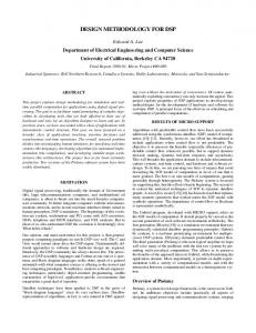
5. RESULTS Area and power of NCOs were investigated with various synthesis runs, with different degrees of hybridization for timing constraints set to implement a ‘fast’ (fCLK ≡ 200 MHz) or a ‘low power’ (fCLK ≡ 20 MHz) version. This systematic study was facilitated by our flexible and fully parametrizable VHDL model. If an optimum number of LUT entries is replaced by CORDIC stages, or vice versa, there is a remarkable decrease both in area and in power dissipation as compared with pure CORDIC or pure LUT solutions. The LUTs were implemented by combinatorial gates, and, alternatively, by using a ROM layout generator. With the generator provided by AMS, ROMs may be generated with a capacity in the range of 2.048 to 524.288 bits. The minimum number of data words which can be processed is 512. Hence the minimum ROM size is 512x19 for the X- as well as for the YLUT (FS = 11), whereas the maximum ROM capacity investigated was 8192 x 19 (FS = 15). 10 Area Total [ mm2 ] 9 200 MHz 8 20 MHz 7 6 5 4 Combinatorial ROM 3 2 1 ROM Generator 0 0 1 2 3 < CORDIC solution area
4 timing
5
6
7
area(ROM)
8
9
10
11
timing(ROM)
12
13
14 15 FS LUT solution >
timing(layout)
Figure 4. Core area in µm² for 0 ≤ FS ≤ 15. The chip was area optimized for 20 MHz clock (‘area’). Best timing performance reached 200 MHz (‘timing’). ‘ROM’ indicates an AMS-ROM for LUT. ‘Layout’ refers to chip areas after layout generation. The core area of the different implementations is shown in Fig. 4. As a reference point, the area for a pure CORDIC-solution
(FGO=16, FW=32 and AW=20) with fCLK = 200 (20) MHz reads, according to the Synopsys area report, 1.89 (1.08) mm². Actual layout sizes after place and route for the 200 MHz solution are given as well. Area estimates are available for combinatorial LUTs in the range of 0≤FS≤13. Larger FS–values require generated ROMs, so employing ROMs as LUT was investigated for 11≤FS≤15. Note that even for FS=15 there are still two CORDIC stages needed, to iterate the LUT-values to the desired precision, i.e. LS=16.
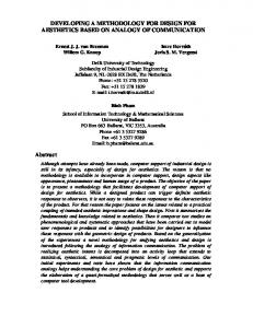
than the add/shift operations in the CORDIC stages. However, increasing LUT size, the gate and wire capacitances to be charged increase as well. Therefore, the gradient of power curves diminishes with increasing FS-values. For FS = 12, for 200 (20) MHz clock power reaches the minimum at 161.9 (11.12) mW. For the pure LUT implementation, the power dissipation of the ROMs is estimated 786 mW at 200 MHz, which again is far above the figures for the hybrid FG architectures reported here.
If a pure LUT-based solution for the FG is to be designed, then two tables for sine and cosine are needed with a word length FGO=16 and an address length AW. Implementing this in ROMs results in an area of 10.93 mm², which is off scale in Fig. 4. Hence, pure LUT solutions are far from offering the area efficiency of hybrid implementations. In the case of combinatorial ROMs, broad area minima are centered around FS=9 for both clock specifications. The minimum area for 200 MHz is 1.13 mm², for FS=9, and, for 20 MHz, 0.68 mm², for FS=8. If diffusion ROMs are implemented, there is a further reduction to 1.07 mm² (200 MHz, FS=11) or 0.75 mm² (20 MHz, FS=11). Note that after place and route, the area curve is shifted, and for a larger LUT portion, the actual chip area is nonlinearly increased as compared to the Synopsys derived results. The minimum is then in the range of FS=7 to 8. The size of the area optimum (FS = 7) is 1,283 x 1.149 mm². As the maximum fCLK we obtain 170 MHz from QuickSimII including back-annotation for this design. So there is a moderate 15% performance reduction due to layout related effects as compared to the Synopsys timing reports. The average clock delay in the design with respect to the master clock is 1.47 ns, whereas the maximum clock skew for the 610 registers is 0.2 ns.
We presented a new hybrid generation scheme for the signal amplitudes for NCO, which combines traditional look-up tables with the algorithmic iterative procedures of the CORDIC algorithm. As the investigations in the paper showed, no technology specific ROM generators are required to implement area and power efficient NCOs. Therefore such hybrid architectures enable technology independent HDL descriptions of high performance, high precision DDFS systems, which allow for full portability and reuse of NCO cells.
6. CONCLUSIONS
The key component of the NCO design flow is a fully parametrizable VHDL model. To get a synthesizable model, the LUT entries originated from the math_real package. They then were written out using textio functions to automatically generate the source code of a package, which contains all the required information as constants. This method is applicable to other mathematical functions as well. The performance of the NCO design was tested by synthesis to a 0.35µm CMOS technology with systematic variations of the nco parameters. Our evaluation of hybrid CORDIC/LUT implementations showed that this approach outperforms traditional pure algorithmic (CORDIC) as well as pure look-up table solutions (LUT) in terms of layout area and power budget.
450
Power Total [ mW ]
7. REFERENCES
400
200 MHz
[1] Thierney, J., Radar, C. M., and Gould, B. A Digital Frequen-
350
cy Synthesizer. IEEE Trans. on Audio and Electroaccustics, vol. AU-19 (1971), 48 -57
300
ROM Generator 250
[2] L. K. Tan, and H. Samueli, “A 800 MHz Quadratur Digital
200
100
Synthesizer with ECL-Compatible Output Drivers in 0.8 µm CMOS”, IEEE J. Solid State Circuits, vol. 30, (1995), 1463 – 1473
50
[3] Bellaouar, A., O´brecht, M. S., Fahim, A. M., and Elmasry,
Combinatorial ROM 150
20 MHz
M. I. Low-Power Direct Digital Frequency Synthesis for Wireless Comunications”, IEEE J. Solid State Circuits, vol. 35, (2000), 385- 390
0 0
1
2
3
4
5
6
7
8
9
10
11
12
13
< CORDIC solution
14
15
FS
LUT solution >
area
timing
area(ROM)
timing(ROM)
[4] Volder, J. E., The CORDIC trigonometric computing techFigure 5. NCO power consumption in mW as function of FS from 0 to 15 (legend c.f. Fig. 4).
nique. IRE Trans. Electron. Comput., vol. 8, (1957), 330 – 334
Fig. 5 shows results for the power dissipation of the various NCO implementations. Obviously, high performance adder/subtractors in the CORDIC stages play an essential role for the power budget. The pure CORDIC implementation (FS = 0) with fCLK = 200 (20) MHz consumes 415 (33) mW. If the 20 MHz and the 200 MHz implementations are compared, power will not scale with fCLK, as the high speed version (200 MHz) uses fast adders as carry look ahead, whereas the power-optimized slower (20 MHz) solution uses simple and power efficient carry ripple adders.
[5] Timmermann, D., Rix, B., Hahn, H., and Hosticka, B. J. A
If CORDIC stages are replaced by LUT, power consumption decreases, as the access to LUT data implies less switching activity
1
CMOS Floating-Point Vector-Arithmetic Unit. IEEE J. Solid State Circuits, vol. 29, (1994), 634–639
[6] M. Dachroth, M., Hoppe, B., Meuth, H., and Steiger, U. H. High-Speed Architecture and Hardware Implementation of a 16-bit 100-MHz Numerically Controlled Oscillator. Proc. of ESSCIRC’98, (Den Haag, 1998), 456 – 459
On leave from Institute of Electron Technology, Warsaw, Poland