47.3
Dynamic Global Buffer Planning Optimization Based on Detail Block Locating and Congestion Analysis 1
Yuchun Ma1, Xianlong Hong1, Sheqin Dong1, Song Chen1, Yici Cai1, C.K.Cheng2, Jun Gu3 2 Department of Computer Science & Technology, Tsinghua University, Beijing, China,100088 Department of Computer Science and Engineering, University of California,San Diego CA 92093-0114,USA 3 Department of Computer Science, Science & Technology University of HongKong
[email protected];
[email protected] buffers will be inserted on a single chip in the 70nm technology[1]. Since buffers are implemented by transistors, they cannot be placed over the existing circuit blocks. Placing a large number of buffers between circuit blocks could significantly impact the chip floorplan. Therefore, it is necessary to start buffer planning as early as possible. It is very useful that a good planning of the block positions can be obtained during the floorplanning stage so that buffers can be inserted wherever needed in the later routing stages.
ABSTRACT By dividing the packing area into routing tiles, we can give the budget of the buffer insertion. And the detail locating of the blocks in their rooms can be implemented for each iterations during the annealing process to favor the later buffer planning. The buffer insertion will affect the possible routes as well the congestion of the packing. The congestion estimation in this paper takes the buffer insertion into account. So we devise a buffer planning algorithm to allocate the buffer into tiles with congestion information considered. The buffer allocation problem is formulated into a net flow problem and the buffer allocation can be handled as an integral part in the floorplanning process. Since there is more freedom for floorplan optimization, the floorplanning algorithm integrated with buffer planning can result in better performance and chip area.
1.1 Previous Works There are several previous works addressing the interconnect issues in floorplanning design. Cong[2] define the term “feasible region” (FR) of a net, that is, the largest polygon in which a buffer can be inserted such that the timing constraint can be satisfied. Sarkar[3] added the notion of independence into feasible regions so that the feasible regions of different buffers on a net can be computed independently. These two papers gives the basic idea of Feasible Region, based on which they proposed the buffer planning algorithms. But both of their methods take complex scanning to obtain the feasible buffer insertion sites. Tang and Wong[4] propose an optimal algorithm based on net flow to assign buffers to buffer blocks assuming that only one buffer is needed per net. Alpert et al.[5] make use of tile graph and dynamic programming to perform buffer block planning, while they propose that buffers should be allowed to be inserted inside macro blocks. But all of these algorithms are based on fixed die placement and it is difficult to embed those methods into the iterations of the floorplanning process because of the complexity of those algorithms. Unfortunately, the fixed placement is likely to generate some timing-constraint violations which are beyond repair unless the topological relation between blocks can be changed. Sham[6] proposed a routability driven floorplanner while the buffer insertion are assumed to be inserted at a flexible interval from each other for long enough wires. Therefore, the buffer insertion is just estimated by probabilistic budget, while the buffer blocks are not allocated in Ref.[6]. Hence, to create a performance-feasible floorplan, a performance-driven floorplanner that simultaneously considers area and buffer block insertions is needed. Although many
Categories and Subject Descriptors B.7.2 [Integrated Circuits]: Design Aids – Placement and Routing
General Terms Algorithms, Performance, Design.
Keywords Floorplanning, Routability, Congestion, Buffer Insertion.
1. INTRODUCTION Due to the recent advances in VLSI technology, the number of transistors in a design is increasing rapidly and so are their switching speeds. This has increased the importance of the interconnect delay in the overall performance of a circuit. Many techniques are employed to reduce interconnect delay. Among them, buffer insertion has shown to be an effective approach to achieve timing closure. As transistor count and chip dimension get larger and larger, more and more buffers are expected to be needed for high performance. It was projected that over 700K Permission to make digital or hard copies of all or part of this work for personal or classroom use is granted without fee provided that copies are not made or distributed for profit or commercial advantage and that copies bear this notice and the full citation on the first page. To copy otherwise, or republish, to post on servers or to redistribute to lists, requires prior specific permission and/or a fee. DAC 2003, June 2-6, 2003, Anaheim, California, USA. Copyright 2003 ACM 1-58113-688-9/03/0006…$5.00
This work is supported by the National Natural Science Foundation of China 60121120706 and National Natural Science Foundation of USA CCR-0096383, the National Foundation Research(973) Program of China G1998030403, the National Natural Science Foundation of China 60076016 and 863 Hi-Tech Research & Development Program of China 2002AA1Z1460, the National Doctoral Foundation of China 20020003008.
806
approaches have been proposed to make use of the dead space for buffer insertion, few of them optimize the buffer planning by changing the distribution of the dead-space in the placement.
E
E
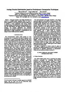
1.2 Our Contributions Previous methods of buffer planning are based on the fixed blocks. We have found that by changing the positions of the blocks within their rooms will not affect the total area and the topological relations, but the buffer insertions may be optimized. In our floorplanner, we will divide the packing area into routing tiles and we can give the budget of the buffer insertion at each tile. Therefore, we devise a novelty method of the detail process of locating the blocks in their rooms to favor the buffer insertions. The dead spaces in each tile can be computed.
(a) room partition
Fig.2. room partition( E is the necessary empty room) floorplan area, wire length and the timing violations are minimized and the buffers can be inserted in the dead spaces as much as possible and the congestion between routes can be minimized. We assume that the wires are routed over-the-cell. The general flow of our algorithm is given in Fig.1. Our algorithm consists of three key steps: block planning, buffer planning and solution perturbation and evaluation.
The buffer insertion will influence the routing ways greatly. So we estimate the congestion information based on 2-bend routes with some blocked tiles considered. This method is very effective since we can use the routes matrix to figure out all the possible routes instead of computing all the routes by scanning the tiles. Taking advantage of the buffer budget and congestion estimation, the buffer planning algorithm is based on net flow method to optimize both the congestion and the buffer insertion. To speed up our algorithm, the simulated annealing process is divided into two phases: timing optimization phase and buffer insertion phase.
The dead spaces besides the blocks will affect the insertion of buffers. Traditional room-based floorplanner will pack the blocks at the lower-left corner or the center of the blocks’ rooms. Thus the dead spaces are distributed without considering the buffer insertion demands. Different from the traditional block planning method, to favor the buffer planning, we firstly pack the blocks by given solutions to obtain their room partitions, then the positions of the blocks are determined by the buffer budget in whole packing area. And the later buffer planning is based on the result of the detail locations of the blocks. The congestion information is estimated taken into account the buffer requirement for all nets. The buffers are allocated based on net flow algorithm considering both buffer position and the congestion estimation.
The rest of the paper is composed as follows: Sect.2 gives the overview of our floorplanner; Sect.3 gives the budget of the buffer insertion and the floorplanning algorithm to locate the circuit blocks in their rooms. The buffer planning algorithm and the two-phase annealing process are described in Sect.4 and Sect.5. The experimental results are shown in Sect.6. Finally, the conclusion is given.
3. Floorplanning Algorithm In the room-based representation such as (BSG, SP, CBL, Slicing), the blocks are packed within the range of the rooms. If we can move the blocks in their room, the buffer insertion will be optimized since it can leave much more dead space where the buffers are needed.
2. OVERVIEW OF OUR FLOORPLANNER In this paper, we concentrate on the buffer planning problem with the floorplanning. The insertion of buffers should be in the dead spaces between circuit blocks. We seek a floorplanning methodology to produce the optimal floorplan such that the
3.1 Rooms in the packing The chip can always be dissected into small rectangles, denoted as room(Fig.2(a)). Given an n-block set, it divides the chip into at least n rooms and assigns no more than one block to each room. And the topological relations between the rooms depend on the representations of the floorplanning. Most of the rooms are not held entirely by the circuit blocks. Therefore, some dead-spaces may be generated. And in the non-slicing structure, some rooms may contain no circuit blocks but dead space so called necessary empty room (Fig.2).
Specs of blocks, nets, timing Block planning Room partition
Initial Solution of annealing process
Buffer budget Block planning Detail blocks locating Solution perturbation and Buffer planning decrease the temperature Solution evaluation
No
(b) move blocks within rooms
Definition 1: the necessary empty room is the empty room without circuit block and it can not be removed by merging with the other rooms.
Buffer planning
The blocks can be moved within their rooms while the area and the topological relations remain. The dead space in necessary empty room should be fixed and the dead space in the block room can be redistributed by moving the block within its room(Fig2(b)).
Congestion estimation Buffer allocation
Stop annealing ?
3.2 Budget of buffer insertion
Yes
Each driver/buffer is modeled as a switch-level RC circuit[8] and the Elmore delay formula[7] is used for delay computations.
Fig.1. Overall algorithm
807
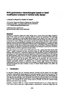
pins are located at the center of the tiles. It is very effective to figure out the possible buffer insertion tiles for different length. As shown in Fig.3, there is a sub-packing with 5 blocks and 2 nets between them. Three possible buffer tiles(B) for net(S,T) and two possible buffer tiles(b) for net(s,t) are shown in Fig.3(b).
The notation for the physical parameters of the interconnect and buffer we use in this paper is as follows: r
wire resistance per unit length
c
wire capacitance pre unit length
Tb intrinsic buffer delay
Each tile will have more than one buffer inserted. And each buffer may have several possible insertion tiles. Thus we devise a weight for each tile. Assuming that the probability of each possible insertion tile for a buffer in the net are equal, Bi is a buffer of a net and it has Ki possible insertion tiles, which includes tile (x,y). Thus the probability P(x,y,Bi) that the buffer
Cb buffer input capacitance Rb buffer output resistance CL sink capacitance; Rd driver resistance; Ln the length of sink-source net N(two pin net)
Bi is inserted at tile (x,y) is: P(x,y,Bi) =
The optimal locations of the k buffers for delay minimization of the net as shown in [3] are
x i* = (i − 1) y *L + x *L
i ∈ {1,2,...k }
3.3 Detail locating of blocks
(1)
To insert the buffers as much as possible, the dead spaces resource should be allocated as needed. Since the blocks can be moved within their rooms, the strategies of how to place the blocks in their rooms will affect the total packing performance. With the budget of the buffer insertion, we introduce a novelty method to place the blocks in their room to favor the buffer insertion. First of all we give the weight for each tile(x,y). Suppose that BUFF(x,y) is the set of all the buffers which can be inserted in tile(x,y)
Where
x *L =
k ( Rb − Rd ) (C L − C b ) 1 ( Ln + ) + k +1 r c
y *L =
( R − R d ) (C L − C b ) 1 + ( Ln − b ) k +1 r c
The minimum number of buffers to meet the delay constraint Treq for an interconnect of length l is k min
− K − K 2 − 4K K 5 4 6 5 = 2K 4
Weight(x,y) =
(2)
K 4 = Rb C b + Tb K 5 = ( rC b + cRb )l + Tb + R d C b + Rb C L − Treq r c − (C b − C L ) 2 − ( Rb − R d ) 2 2c 2r
DS_ratio(x,y) =
A_Tile is the area for each tile.
To budget the buffer insertion, we divide a floorplan into a set of 2-dimensional array of routing tiles. According to formula (1), the optimal position for buffer insertion is only affected by the wire length between source and sink. We assume that the
u _ budget ( Ri) =
B b
B
S
b B s
t
(b) the buffer budget 1
B
Object:
3
2
B b
5
Min
n
∑ u _ budget ( Ri )
i =1
We have partitioned the packing into rooms, and the budget of buffer insertion are independent in each room. Therefore we can handle the room one by one. As shown in Fig.4, since the tile position is limited in the rooms, we restrict the lower-left corner of the circuit blocks should be located at the tiles. To facilitate the computation, the problem is handled in two directions, one is vertical and the other is horizontal. At first, we can move the
4
T
(c)detail locating of blocks
∑ (Weight ( x, y ) * (1 − DS _ ratio( x, y ))
( x , y )∈T _ cov ered ( Ri )
In order to optimize the buffer insertion, the unused budget should be minimized, therefore the problem can be described as:
T
s
(a) the room partition
Therefore if tile(x,y) is covered entirely by the circuit blocks, DS_ratio(x,y)=0 and if tile(x,y) is not covered by the circuit blocks at all, DS_ratio(x,y)=1. Thus the object should be to decide the position of the circuit blocks and the buffer budget of the covered tiles is minimized. We define the unused budget in Room Ri as:
B
t
b
ADS ( x, y ) A _ Tile
Where ADS(x,y) is the area of dead space in (x,y)
1 rcl 2 + ( rC L + cR d )l + R d C L − Treq 2
S
∑ P( x, y, Bi)
Bi ∈BUFF ( x , y )
Suppose that the rooms in the packing are {R1….Rn}. Since the buffer insertion should avoid the circuit blocks, Suppose that T_Covered(Ri) is the set of the tiles covered by circuit block in room Ri. Some tiles along the circuit block boundary may not be covered entirely. We define the dead space ratio in each tile is
where
K6 =
1 Ki
(d) dead space partition
Fig.3 detail location of blocks
808
should be reduced. Thus we should count only the routes passing
0.4
0.4
Table 1 Routes matrix
0.2
0.2
0.3
0.3 1.2
0.6
1.2
0.6
(a) u_b= 1.2*1+0.6*1+0.2*0.6 (b) u_b = 0.3*1.0+0.4*0.6=0.54 +0.3*0.5=2.07 Fig.4. the location of block in one room block by the size of tile in the vertical direction to decide the vertical position. Then we move the block horizontally to fix the horizontal position. At the same time, the dead spaces in each tile are fixed.
#routes
0