Dynamic Performance of Current Controllers for Grid-connected Voltage Source Converters under Unbalanced Voltage Conditions Massimo Bongiorno, Student Member, IEEE, Jan Svensson, Member, IEEE and Ambra Sannino, Member, IEEE1
Index Terms - power quality, shunt-connected VSC, power electronics, custom power.
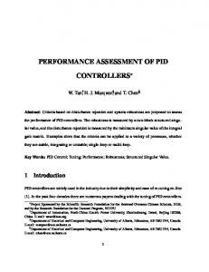
I. INTRODUCTION Grid-connected forced-commutated Voltage Source Converters (VSCs) are becoming more and more common, both at transmission and distribution levels, for applications such as wind power plants (Fig.1 displays a full power converter system), active front-end for adjustable speed drives, HVDC transmission and custom power devices. Benefits of using VSCs are sinusoidal currents, high current bandwidth, controllable reactive power to regulate power factor or bus-voltage level and minimize resonances between the grid and the VSC. These characteristics, which are highly desirable in grid-connected applications, can be obtained by using a high-performance current controller (CC) for the VSC, such as the one presented in [1]. The CC controls the instantaneous active and reactive current to the grid. However, a CC designed as in [1] by only considering positive-sequence components can provide high performance during normal operating conditions of the grid, but will not perform well under unbalance conditions [2]. Unbalance can be a steady-state phenomenon, due to uneven distribution of single-phase loads on the three phases of the distribution system, or appear in the network temporarily, due to faults. Under unbalanced conditions, sinusoidal and balanced currents can be obtained by choosing a high sampling frequency. However, in high power applications the sampling frequency should be kept low to avoid an increase in losses. Moreover, if the dc-link voltage is not stiff, it will still ripple with twice the grid frequency. Otherwise, the dc-link voltage Massimo Bongiorno and Ambra Sannino are with the Department of Electric Power Engineering, Chalmers University of Technology, SE - 41296 Gothenburg, Sweden (e-mail:
[email protected],
[email protected]). Jan Svensson is with ABB Power Technologies, SE - 41296, Gothenburg, Sweden (e-mail:
[email protected])
can be controlled to be constant, but then the grid currents will be unsymmetrical [3]. For the grid-connected VSC it is important to keep the line currents and the dc-link voltage within their allowed values in order to avoid tripping the VSC when a fault/transient occurs on the grid. Since the dc-link voltage is controlled via an outer cascade-loop, the inner current control loop must have a high performance in order to keep a high availability of the VSC system during grid disturbances. By improving the controller to make it capable of handling steps in both positive and negative sequence components (the VSC typically uses a three-wire system, so the zero-sequence component can be disregarded), the performance of the system under unbalanced conditions can be improved without significant increase in cost. Different CCs have been proposed, which use sequence components to deal with unbalanced grid conditions. In reference [4] positive and negative sequence components are separated, but only the positive sequence is controlled by a CC implemented in the positive synchronous reference frame (SRF). Reference [5] uses two different CCs for the two sequence components together with a dc-link voltage controller based on instantaneous active and reactive power. With this arrangement, steady-state cancellation of the voltage ripple is obtained. However, in [5] the performance is shown only in steady state and in [4] the method to separate the positive and negative sequence components is not described. When investigating the dynamic performance, the method for sequence separation used is expected to have a great impact. In this paper, the transient performance under balanced and unbalanced conditions of three different CCs for shuntconnected VSC is investigated and compared. A sequence detection method that implies a delay of one quarter of line cycle is used. The dc-link voltage is constant and steps in the reference currents are applied in order to test the transient response of the system. Simulation and experimental results are shown for all three CCs. − − −
Grid + e1(t )
i1(t)
∼
∼ ∼
−
+
u3 (t) L R
3 PWM
sw(t )
sample and hold
Vector Current Controller + Dc-link Voltage θ (k) estimator Controller
i (αβ )(k) 2
+
udc(t ) −
3/2
2
dc-link Rectifier
iv (t) idc(t)
u2(t)
i3(t)
sample and hold
e(αβ )(k)
VSC
u1(t)
i2(t)
+ e2 (t ) + e3(t )
Line Filter
∼ =
Abstract- The increasing use of Voltage Source Converters (VSCs) in grid-connected applications at distribution levels requires control methods that achieve high performance not only during normal operating conditions of the grid, but also under unbalance conditions. These can occur temporarily, due to faults, or permanently, due to uneven distribution of single-phase loads on the three phases of the distribution system. In this paper, three different current controllers for shuntconnected VSC are investigated and compared under unbalanced conditions. The dc-link voltage is constant and steps in the reference currents are applied in order to test the dynamic performance of the system. Simulation and experimental results are shown for all three controllers.
Generator
G Turbine
idc(k) udc(k) θ (k)
Fig.1. Grid-connected VSC in variable-speed wind turbine application.
II. SYSTEM CONFIGURATION The system configuration of the VSC connected to the grid by an L-filter is shown in a wind power application in Fig.1. The resistance and the inductance of the line filter are denoted by R and L, respectively. The phase voltages and currents of the grid are denoted by e1, e2 and e3 and i1, i2 and i3, respectively. The phase voltages of the VSC are denoted by u1, u2 and u3. The grid currents and the grid voltages are sampled and transformed into vectors in the fixed two-axis αβ-coordinate system and then into the rotating dqp- or dqn-coordinate system by utilizing the transformation angle θ which is obtained from the phase-locked loop (PLL) that tracks the grid voltage. The d-axis of the dqp-frame is synchronized with the grid voltage vector. The dqp-frame rotates with the grid angular frequency in the positive direction and the dqn-frame rotates with the grid angular frequency in the negative direction. The CC tracks the reference currents by generate a proper reference voltage in the rotating coordinate system. The reference voltage vector from the controller (denoted by u*) is transformed into the three-phase system. To take full advantage of the dc-link voltage udc, triplen harmonics are added to the reference voltage before entering the PWM block. The grid frequency is denoted by f and the sampling and the switching frequencies are denoted by fs and fsw, respectively. The used system parameters are presented in Table I. TABLE I SYSTEM PARAMETERS E=400 V=1 pu (ac)
udc=600 V=1 pu (dc)
L =2 mH=0.1 pu f=50 Hz
R= 24.8 mΩ=0.01 pu fsw =5kHz
(dq ) I base =40 A
In this section, the three different CCs will be introduced. The first two controllers are implemented in the positive SRF, also called dqp-frame. The third CC uses both positive SRF and negative SRF (dqn-frame). Vector Current Controller (VCC) The first controller, presented in [1], is denoted as VCC. Equation (1) describes the control system in the synchronous reference frame, while its block scheme is shown in Fig.2. (k ) = e
( dq )
+ k p (i
( k ) + Ri
( dq )*
( dq )
(k ) − i
(k ) + j
( dq )
(i 2
ωL k
( dq )*
( k )) + ∑ ki (i
(k ) + i
( dq )
( n) − i
θ (k ) (αβ )
2
( dq )*
2
i i
VCC 2e αβ dqp
( dq )
u
( dq )
( dq )*
u dqp αβ 2 θ (k )
CC 2 in positive SRF
2 αβ dqp ( dq ) i
(αβ )*
u
2
(123)*
3
3
PWM sw(t ) 3
Fig.2. Block scheme of VCC that uses positive SRF.
B. VCC using feedforward (VCCF) In the second controller, the grid voltage is divided into positive and negative sequence components, but only the positive sequence voltage is used in the CC [4]. The negative sequence grid voltage is directly added to the reference voltage vector, as shown in Fig.3. The equation describing this control system is similar to Eq.(1), where only the positive sequence of the grid voltage is considered. The abbreviation used here is VCCF, where F stands for “feedforward.” (dq )*
VCCF
i ( )* ( dq ) (αβ ) 2 u dq 2 i i αβ 2 dqp 2 CC dqp (dqp ) in αβ θ (k ) e positive SRF (αβ ) 2 SSM dqn e ( ) αβ e dqn 2 θ (k ) 2
+ +
u 2
(αβ )*
2
u 3
(123)*
3
PWM sw(t ) 3
)
The third controller, denoted as “Dual Vector Current Controller” (DVCC), consists of two CCs implemented in the positive and the negative SRF, respectively, as shown in Fig.4. In Eq.(2) and Eq.(3), the expressions of the two CCs are displayed in the positive and negative SRF. Both the grid current and the grid voltage are separated into positive- and negative-sequence components and the controller tracks positive- and negative-sequence reference currents [5]. u ( dqp )* (k ) = e ( dqp ) (k ) + Ri ( dqp ) (k ) + j
ωL 2
(i
( dqp )*
(k ) + i (
dqp )
)
(k ) +
k
+ k p (i ( dqp )* (k ) − i ( dqp ) (k )) + ∑ ki (i ( dqp )* ( n) − i ( dqp ) (n − 1))
(2)
n =1
(k ) +
(1) ( dq )*
2
C. Dual Vector Current Controller (DVCC)
A. Vector Current Controller (VCC)
( dq )*
e
(αβ )
Fig.3. Block scheme of VCCF that uses positive SRF and feedforward of negative sequence grid voltage.
Ibase=23.1 A fs =5kHz
III. INVESTIGATED CURRENT CONTROLLERS
u
observer for compensation of the one-sample delay due to the computation time [6]. To prevent integrator wind-up, backcalculation of the current error is used.
(n − 1))
n =1
where the proportional gain to obtain dead-beat response is equal to k p = L Ts + R 2 and the integral gain is equal to k i = k p Ts Ti . In this paper the integration time constant is set
to Ti = L R . The active and reactive currents are controlled independently of each other with a high bandwidth, even in the overmodulation region by using Smith predictor with a state
u ( dqn )* (k ) = e ( dqn ) ( k ) + Ri ( dqn ) (k ) − j
ωL 2 k
(i
( dqn )*
(k ) + i
( dqn )
)
(k ) +
+ k p (i ( dqn )* (k ) − i ( dqn ) (k )) + ∑ ki (i ( dqn )* (n) − i ( dqn ) (n − 1)) n=1
(3)
i
DVCC
( dqp )*
e
2 (αβ ) 2
θ (k ) i i
2
reported in Table II (the same gains are used for the two sequences in DVCC).
CC 2 e 2 in SSM 2 i ( dqp ) positive SRF
SSM 2 e 2 i ( dqn ) 2
( dqn )
(αβ )
( dqn )*
( dqp )
CC in negative SRF
dqp (αβ )* αβ (123)* u u θ (k ) + 2 3 3 2 dqn + 2 PWM αβ sw(t ) 3
Network model
Strong net
Load
Fig.4. Block scheme of DVCC that uses positive and negative SRF. contactor 1
D. Phase Sequence Separation Method (SSM)
dc - machine
VLT5052
The phase sequence separation method (SSM) used here was first proposed in [7]. When applied on the grid voltages in the fixed αβ-plane, it is defined by the expressions
( (t ) = 0.5( e
) ( t − T / 4))
αβ ) e (pos (t ) = 0.5 e (αβ ) (t ) + je (αβ ) ( t − T / 4)
(4)
αβ ) e (neg
(5)
(αβ )
(t ) − je (αβ )
where T is the period time of the grid voltage. The proposed method implies delaying the signal by one fourth of period at the fundamental frequency (in this case, 5 ms). The positive and negative sequence components thus obtained are then transformed into the dqp- and the dqn-frame, respectively, where they appear as dc quantities. A negative sequence component would give a double-frequency signal in the dqpframe. The same holds for a positive sequence component in the dqn-frame. III. SIMULATION AND EXPERIMENTAL RESULTS A. Experimental setup All three controllers presented here have been tested both in simulations, using the simulation program PSCAD/EMTDC, and experimentally in balanced and unbalanced conditions by applying steps in the reference active and reactive currents. However, only steps in the reactive current reference will be shown here. A scheme of the experimental setup is given in Fig.5. The laboratory set up consists of a Danfoss VLT5052 converter and the control computer is a DSPACE 1103. The system parameters are presented in Table I. A dc machine rated 700 V, 60 A, supplies the dc link of the VSC. The VSC was connected to a 400V analog model of a transmission line. This is composed of six identical Π-sections in series, each constituted by a series inductor L1 = 2.05 mH and two shunt capacitors C1/2 = 46 µF, as indicated in Fig.5. The Π-section to the right in Fig.5 represents in fact the series of the remaining Π-sections. In order to absorb an unbalanced current from the mains, the network model was loaded with an unbalanced load constituted by a three-phase resistor of 8.8 Ω (18 kW) together with a 4.1 Ω resistor connected between the phases 1 and 2. B. Performance with balanced grid voltage A first set of tests was carried out with balanced grid voltage applied to the VSC with all three CC types. The parameters used for the PI-controllers in the three cases are
filter
contactor 2 grid voltage
optical wires
DS1103
Fig.5. Scheme of laboratory setup and 400V analog network model. TABLE II CONTROLLER PARAMETERS Controller VCC, VCCF DVCC
kp 10.01 (deadbeat) 7.01 (70% of deadbeat)
kI 24.8·10-3 17.36·10-3
In order to have a stiff and symmetric ac voltage, the VSC was connected directly to the strong network by closing contactor 1 in Fig.5, with contactor 2 open. Therefore the grid voltage will not be affected by the current from the VSC. Simulated and measured dq-currents for the VCC are shown, respectively, in Fig.6 and Fig.7 when at the time 0.02 s a step from 0.125 to 0.5 pu in reactive current reference is applied. The actual current tracks the reference current with only two samples delay and the performance can be regarded as very high. It is possible to observe that, due to the harmonics in the supply, the measured current is affected by small ripples around the steady-state value. The results for the VCCF in Fig.8 and Fig.9 also show a very good performance when a step in the reactive reference current is applied. The results for the DVCC instead show that the actual current tracks the reference current with a significant time delay. The simulated and measured dq-currents for the positive phase-sequence are shown in Fig.10 and Fig.11, respectively, when a step in the positive phase-sequence reactive current reference is applied. The actual current takes one quarter of the line cycle to track the reference current, due to the phase-sequence detection, and a cross-coupling component can be noticed in the d-current. The cross-coupling component is however not very large (the scale of the plot has been enlarged to make it visible). The negative-sequence dq-currents shown in Fig.12 and Fig.13 are affected by significant cross coupling, due to the sequence detection.
0.5 current [pu]
current [pu]
0.5 0.375 0.25 0.125 0 0.02
0.04
0.06
0.08
0.5 0.31 0.125 −0.06 0.02
0.04 time [s]
0.06
0.08
0
0.02
0.04 time [s]
0.06
0.08
0.5
0.125
0.5
current [pu]
current [pu]
0.06
Fig.10. Simulated d- (top) and q-current (bottom) of positive-sequence for DVCC with balanced grid voltage. Steps in iqp reference.
0.5 0.375 0.25 0.125 0
0.375 0.25 0.125 0
0
0.02
0.04
0.06
0.08
0
0.02
0.04
0.06
0.08
0
0.02
0.04 time [s]
0.06
0.08
0.69
current [pu]
0.69
current [pu]
0.04
0.31
0.08
Fig.6. Simulated d- (top) and q-current (bottom) for VCC with balanced grid voltage. Steps in reactive current reference.
0.5 0.31 0.125 −0.06
0.5 0.31 0.125 −0.06
0
0.02
0.04 time [s]
0.06
0.08
Fig.7. Measured d- (top) and q-current (bottom) for VCC with balanced grid voltage. Steps in reactive current reference.
Fig.11. Measured d- (top) and q-component (bottom) of positive-sequence current for DVCC with balanced grid voltage. Steps in iqp reference.
0.5
0.25
0.375
current [pu]
current [pu]
0.02
−0.06 0
0.25 0.125 0 0
0.02
0.04
0.06
0.125 0 −0.125 −0.25
0.08
0.69
0
0.02
0.04
0.06
0.08
0
0.02
0.04 time [s]
0.06
0.08
0.25
0.5
current [pu]
current [pu]
0 0.69 current [pu]
current [pu]
0.69
0.31 0.125 −0.06 0
0.02
0.04 time [s]
0.06
0.125 0 −0.125 −0.25
0.08
Fig.8. Simulated d- (top) and q-current (bottom) for VCCF with balanced grid voltage. Steps in reactive current reference.
Fig.12. Simulated d- (top) and q-component (bottom) of negative-sequence current for DVCC with balanced grid voltage. Steps in iqp reference.
0.5
0.25
0.375
current [pu]
current [pu]
0.25 0.125 0
0
0.25 0.125 0 0
0.02
0.04
0.06
0.125 0 −0.125 −0.25
0.08
0.69
0
0.02
0.04
0.06
0.08
0
0.02
0.04 time [s]
0.06
0.08
0.25
0.5
current [pu]
current [pu]
0.375
0.31 0.125 −0.06 0
0.02
0.04 time [s]
0.06
0.08
Fig.9. Measured d- (top) and q-current (bottom) for VCCF with balanced grid voltage. Steps in reactive current reference.
0.125 0 −0.125 −0.25
Fig.13. Measured d- (top) and q-component (bottom) of negative-sequence current for DVCC with balanced grid voltage. Steps in iqp reference.
Simulated and measured currents for the VSC with the VCC subjected to the unbalanced grid voltage displayed in Fig.14 are shown in Fig.16 and Fig.17, respectively, when applying a step change on the reference of the reactive current. The 100 Hz oscillation of the actual current is visible both in steady state and during the step. The current flanks are not as steep as in the previous case under balanced voltage because of the reduced controller gain. Moreover, there is an oscillation of the measured current (not present in the simulated one) during the positive and negative flanks, which is due the fact that the voltage is not stiff in this case.
current [pu]
0.5 0.375 0.25 0.125 0
current [pu]
To create the unbalance in the grid voltages, contactor 2 was closed with contactor 1 open. The unbalanced current circulating the Π-sections of the network model creates the three-phase voltage waveform shown in Fig.14 at the VSC terminals, which is denoted by grid voltage. The same unbalance has been reproduced for the simulations. The grid voltage in the dq-coordinate system is shown in Fig.15. The unbalance is 10.9%. Due to the weaker supply, the controller gain of the CC is slowed down as compared with the previous experiments. The gain of the CC is set to 70% of deadbeat gain for the VCC and the VCCF. For the DVCC, the controller gain of the CC in the positive and the negative SRF is still 70% of the deadbeat gain.
steady state appears lower than with the VCC. However, the response is not as fast as in the balanced voltage case in Fig.9 because of the reduced controller gain. There is a small overshoot of the response and an oscillation of the current during the positive and negative flanks, again due to the weak supply voltage. A small cross coupling can be noticed in the d-current during the reference current steps.
0
0.02
0.04
0.06
0.08
0
0.02
0.04
0.06
0.08
0.6 0.3 0 −0.3
Fig.16. Simulated d- (top) and q-current (bottom) for VCC with unbalanced grid voltage. Steps in reactive current reference. 0.5
current [pu]
C. Performance with unbalanced grid voltages
0.375 0.25 0.125 0 0
0.02
0.04
0.06
0.08
0
0.02
0.04
0.06
0.08
current [pu]
1
voltage [pu]
0.5
0
0.6 0.3 0 −0.3
−0.5
Fig.17. Measured d- (top) and q-current (bottom) for VCC with unbalanced grid voltage. Steps in reactive current reference.
−1 0.02
0.04 time [s]
0.06
0.08
Fig.14. Measured three-phase unbalanced grid voltages.
current [pu]
0.5
0
0.375 0.25 0.125 0
1.5
0
0.02
0.04
0.06
0.08
0
0.02
0.04 time [s]
0.06
0.08
0.69
voltage [pu]
current [pu]
d−component
1
0.5
0.5 0.31 0.125 −0.06
q−component 0
Fig.18. Simulated d- (top) and q-current (bottom) for VCCF with unbalanced grid voltage. Steps in active current reference. −0.5 0
0.02
0.04 time [s]
0.06
0.08
Fig.15. Measured dq-components of the grid voltage.
The characteristic 100 Hz oscillations denoting unbalance are not present in the dq-currents obtained with the VCCF, shown in Fig.18 and Fig.19 when applying a step change on the reactive current reference. Also, the current ripple in
0.25
current [pu]
current [pu]
0.5 0.375 0.25 0.125
0 −0.125 −0.25
0 0
0.02
0.04
0.06
0.08
0
0.02
0.04
0.06
0.08
0
0.02
0.04 time [s]
0.06
0.08
0.25
current [pu]
0.69
current [pu]
0.125
0.5 0.31 0.125
0.125 0 −0.125 −0.25
−0.06 0
0.02
0.04 time [s]
0.06
0.08
Fig.19. Measured d- (top) and q-current (bottom) for VCCF with unbalanced grid voltage. Steps in active current reference.
Fig.21. Simulated d- (top) and q-component (bottom) of negative-sequence current for DVCC with unbalanced grid voltage. Steps in iqp reference.
In some applications like for example a Dynamic Voltage Restorer, where there is a need to control the two sequence components separately [8] and therefore DVCC must be used, an improved performance might be obtained by optimizing the gains for the two controllers for the specific application considered. The choice of a faster SSM, if possible, would also greatly impact the response. current [pu]
0.25 0.125 0
0.02
0.04
0.06
0.08
0
0.02
0.04 time [s]
0.06
0.08
current [pu]
0.69 0.5 0.31 0.125 −0.06
Fig.22. Measured d- (top) and q-component (bottom) of positive-sequence current for DVCC with unbalanced grid voltage. Steps in iqp reference.
current [pu]
0.25 0.125 0 −0.125 −0.25 0
0.02
0.04
0.06
0.08
0
0.02
0.04 time [s]
0.06
0.08
0.25 0.125 0 −0.125 −0.25
Fig.23. Measured d- (top) and q-component (bottom) of negative-sequence current for DVCC with unbalanced grid voltage. Steps in iqp reference.
0.5 0.375 0.25 0.125 0 0
0.02
0.04
0.06
0.08
0
0.02
0.04 time [s]
0.06
0.08
0.69
current [pu]
0.375
0
current [pu]
Still it is possible to observe that there is a cross coupling in the negative sequence dq-currents in Fig.21 and Fig.23 when applying a step to the positive-sequence q-current but is unchanged compared with the case of the balanced supply voltage. It is interesting to observe that due to the presence of the sequence diction and then to the better control of the filter current, the current ripple due to the harmonics present in the grid has been reduced compared with the results obtained with the VCCF.
current [pu]
0.5
The positive-sequence dq-currents in the dqp-frame obtained with the DVCC are shown in Fig.20 and Fig.22. A step in the positive-sequence reactive current reference is applied. As expected, the transient performance of this control system is the same as in case of balanced conditions of the grid voltage. The actual current tracks the reference but, as noticed in the previous set of results, is affected by a 5 ms delay due to the adopted sequence detection. However, as for the other two control systems, the weaker supply voltage influences the response.
0.5 0.31 0.125 −0.06
Fig.20. Simulated d- (top) and q-component (bottom) of positive-sequence current for DVCC with unbalanced grid voltage. Steps in iqp reference.
VI. CONCLUSIONS In this paper, three different current controllers for shuntconnected VSC have been investigated and compared under balanced and unbalanced conditions. With a constant dc-link voltage, steps in the reference currents have been applied in order to test the dynamic performance of the system. Both simulation and experimental results have been shown for all three controllers. It has been demonstrated that, with the VCC designed by only considering positive sequence components, the dqcurrents under unbalanced grid voltage are affected by an oscillation at double the power frequency. By feeding the same controller only the positive-sequence component of the grid voltage in the VCCF, the response is improved and the actual current tracks the reference current with almost no delay. The DVCC, where both voltages and currents are separated into their sequence components and two separate current controllers are used, showed a more sluggish response, mostly due to the delay introduced by the sequence separation. The VCCF showed the best performance. Nevertheless, in some applications the current sequence components have to be controlled separately and therefore the DVCC must be used.
REFERENCES [1]
[2]
[3]
[4]
[5]
[6] [7]
[8]
R. Ottersten, J. Svensson, “Vector current controlled voltage source converter − deadbeat control and overmodulation strategies,” IEEE Trans. on Power Electronics, Vol. 17, No.2, March 2002, pp.279-285. P.N. Enjeti, S.A. Choudhury, “A new control strategy to improve the performance of a PWM AC to DC converter under unbalanced operating conditions,” IEEE Transactions on Power Electronics, Vol.8, No.4, Oct. 1993, pp.493-500. G. Saccomando, J. Svensson, “Transient Operation of Grid-connected Voltage Source Converter Under Unbalanced Voltage Conditions,” 2001 IEEE Industry Applications Conference, 36th IAS Annual Meeting, September 30 - October 5, 2001, Chicago, Illinois USA, pp. 2419-2424. P. Rioual, H. Pouliquen, J-P. Louis, “Regulation of a PWM Rectifier in the Unbalanced Network State Using a Generalized Model,” IEEE Trans. on Power Electronics, Vol. 11, No. 3, May 1996, pp. 495-502. H.-S. Song, K. Nam, “Dual Current Control Scheme for PWM Converter Under Unbalanced Input Voltage Conditions,” IEEE Trans. on Industrial Electronics, Vol. 46, No. 5, October,. 1999, pp. 953-959. K. J. Åström, B. Wittenmark, Computer-controlled Systems: Theory and Design, 2nd Ed., Prentice Hall, Englewood Cliffs, NJ, 1990. T.-N. Le, “Kompensation schnell veränderlicher Blindströme eines Drehstromverbrauchers,” etzArchiv, Bd. 11, (1989), H. 8, pp. 249-253, (in German). H. Awad, J. Svensson, “Double Vector Control for Series Connected Voltage Source Converters,” in Proc. of IEEE Power Engineering Society, Winter Meeting, vol.2, pp.707-712.