This paper presents a novel circuit that combines reso- nant tunneling diodes with MOSFETs to create a very compact and high-speed flip-flop implementation.
ECCTD’01 - European Conference on Circuit Theory and Design, August 28-31, 2001, Espoo, Finland
Edge-Triggered Flip-Flop Circuit Based on Resonant-Tunneling Diodes and MOSFETs �
Shriram KULKARNI and Pinaki MAZUMDER Abstract This paper presents a novel circuit that combines resonant tunneling diodes with MOSFETs to create a very compact and high-speed flip-flop implementation. This edge-triggered flip-flop circuit offers smaller circuit size and area as compared to a true single-phase CMOS flipflop. The circuit can operate at lower supply voltage as compared to a conventional CMOS flip-flop and provides better noise immunity through isolation of dynamic storage nodes. 1
φ
d
Introduction
RTD-based circuits have unique self-latching properties [1]. However, until the present time there have been no true single phase clocked (TSPC) edge-triggered flipflop circuit implementations using RTDs. It is well known that edge-triggering is commonly required in VLSI circuits for accurately sampling an input at a clock edge so that further circuits are immune to any variations in the input signal that might otherwise lead to false evaluation. Here we present the design of a family of edge-triggered flip-flops using RTDs and MOSFETs [2].
φ
(a)
�
V �
2
Edge-Triggered True Single Phase QMOS FlipFlop
q
2.5
φ
D �
Q
2
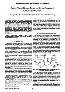
Fig. 1(a) is a schematic diagram of a QMOS negative 1.5 edge-triggered D flip flop circuit. It uses an RTD latch 1 followed by a CMOS TSPC output stage [3]. When the clock signal is high, the access transistor to 0.5 the RTD-pair latch is turned on and the latch node tracks the input voltage. At this time the clock transistor in the 0 second stage is turned off and hence the output is unaffected by any changes in the input. When the clock -0.5 ns 1.5 1 0.5 0 signal goes low, the access transistor to the RTD latch is turned off. The RTD-pair latches the value of the (b) input at its common terminal. The clocked inverter is turned on, and following the inversion of the output stage, the node reflects the value of the input at the Figure 1: Negative edge-triggered QMOS TSPC D flip time of the clock edge. Simulation traces of the QMOS flop (a) circuit diagram, (b) simulation traces. TSPC D flip-flop are shown in Fig. 1(b). Since the QMOS TSPC flip-flop contains three MOS transistors �
�
�
�
�
�
This research has been supported in part by grants from DARPA and ARO MURI. Department of Electrical Engineering and Computer Science, The University of Michigan, Ann Arbor, MI 48109-2122 USA �
I-185
in series in the output stage, the threshold voltage drops of the PMOS and NMOS devices require the TSPC D flip-flop to operate at a larger supply voltage as compared to other QMOS flip-flop topologies. The D flip-flop can be easily modified to operate as an S-R flip-flop. The circuit diagram of a QMOS S-R flipflop is illustrated in Fig. 2(a). Fig. 2(b) shows a positive edge-triggered QMOS T flip-flop. The T flip-flop uses an XOR gate to generate the controlling feedback from the flip-flop output. An XOR gate can be implemented using just one RTD and three n-type FETs [4] and hence we achieve an extremely compact implementation of a T flip-flop.
flops by adding a p-type MOSFET between the power output whose gate is controlled by supply and the an active low preset input. Similarly, asynchronous reset can be achieved by connecting an active high reset signal to the gate of an n-type MOSFET connected output. Fig. 3 shows the between ground and the schematic diagram of a QMOS positive edge-triggered D flip flop with asynchronous reset and preset. �
�
p
d
s �
φ
φ
q
r
q
Figure 3: Circuit diagram of a QMOS positive edgetriggered D flip flop with asynchronous reset and preset.
φ r
3 Comparison of QMOS and CMOS Flip-Flop Circuits (a)
Q
φ
Q
In this section, we present a comparison between QMOS flip-flop circuits and CMOS flip-flop circuits based upon comparison of the circuit network topologies. Of prime interest using these approximate analyses is comparison of the timing behavior, area, and power consumption of the flip-flop circuits. Five different flip-flop circuits are considered for comparison, including two QMOS flip-flops and two CMOS flip-flops. These are: 1) C MOS master-slave flip-flop, 2) Bistable QMOS master-slave flip-flop, 3) CMOS TSPC flip-flop, and 4) QMOS edge-triggered TSPC flip-flop.
T φ
3.1
Flip-flop parameters
Three timing parameters of the flip-flop are of interest. The setup time, , is defined as the time for which the (b) input signal to the flip-flop must have stabilized prior to the arrival of the active clock edge. The hold time, , is Figure 2: Circuit diagram of a QMOS positive edge- defined as the minimum time for which the input signal triggered TSPC (a) S-R flip-flop, (b) T flip-flop. must be stable after the active edge of the clock in order to have correct evaluation. The clock-to-Q delay, , is defined as the propagation delay from the active edge of Positive edge-triggered flip-flops can be derived from the clock to the new valid output of the flip-flop. It is their negative edge-triggered versions by interchanging important to understand the relative importance of these the p-type FET and n-type FET whose gate terminals timing parameters. The minimum delay of a single flipare connected to the clock input. Asynchronous set op- flop stage governs the maximum operating frequency of . The hold time, eration can be added to the above edge-triggered flip- the flip-flop and is given by
�
I-186
�
�
�
�
�
�
�
of the flip-flop must be less than or equal to so the clock is, that a new valid output of a flip-flop does not violate the of the CMOS TSPC flip-flop is hold time of a succeeding stage. Usually, in the pres- dissipation, ence of combinational logic between stages, hold time constraints are easily met and thus the setup time and clock-to-Q delay form the most important timing parameters of a flip-flop. For area comparison, we define 0.6Cn 0.6Cn the area of a flip-flop circuit as the sum of the channel areas of the various MOS transistors. Here, we make an 0.3Cn assumption that RTDs are vertically integrated on top 0.2Cn qmp of source/drain regions of MOS devices and hence do φ not cause additional area overhead. The dynamic power d 0.2Cn 0.6Cn dissipation of the circuits is compared by utilizing the qmn 0.2Cn 0.1Cn fact that dynamic power is proportional to total capacitance of all the nodes switching during operation of the flip-flop. 0.2Cn 0.2Cn
�
�
�
�
A
�
$
B
�
�
:
�
�
'
�
�
�
0
�
�
�
�
'
. Area . Dynamic power .
0
0
�
� $
�
*
�
1
�
�
�
�
�
�
�
*
�
:
�
�
�
�
0.6Cn
q
φ
3.2
�
0.2Cn
0.8Cn
0.2Cn
Comparison method
To compare performance of QMOS and CMOS flip(a) flops, we use the unit transistor delay metric of [5] that has also been used by Rogenmoser to perform a comparative study of CMOS flip-flop circuits [6]. It is assumed that the time to discharge a node through an NMOS transistor equals the time to charge it though 0.6Cn a PMOS transistor that is three times the size of the 0.6Cn , NMOS transistor. The capacitance at the output, 0.3Cn assumed to be that of a unit inverter, composed of unit transistors, can be subdivided as: 1) PMOS gate ca- 0.1Cn 0.15Cn φ Q 0.2Cn , 2) NMOS gate capacitance, , D pacitance, 0.1Cn 0.6Cn and 3) output capacitance of driving PMOS and NMOS 0.2Cn 0.2Cn . To account for other transistor transistors, φ and RTD configurations, the following assumptions are 0.2Cn 0.2Cn made. When two unit NMOS transistors are driving a node, the contribution to the load capacitance is , instead of the mentioned above. Similarly, when two unit PMOS transistors are driving a node, the contribution to the load capacitance (b) . The contribution of the RTD is to the output capacitance is considered the same as a unit NMOS transistor. The normalized delay through Figure 4: Circuit diagram of (a) CMOS TSPC D load capacitance is assumed to be flip flop with annotated node capacitances, (b) QMOS a transistor per . Further, assume that the standard load of the flip- TSPC D flip flop with annotated node capacitances. flop circuits is a similar stage. Also, the area of a unit and that of a PMOS transistor is NMOS transistor is Fig. 4(b) shows the circuit diagram of a QMOS edge. triggered TSPC D flip-flop with annotated load capacitances. The setup time of the QMOS TSPC flip-flop 3.3 Flip-flop network topology comparison . The propagation is, Fig. 4(a) shows the circuit diagram of a CMOS TSPC delay of the QMOS TSPC flip-flop is, . The area of the QMOS D flip-flop with annotated load capacitances. The setup . Dynamic power dissipation, time for the TSPC flip-flop is measured as the maximum TSPC flip-flop is or . of the delay from the data input to the To summarize the flip-flop comparisons, the results nodes. Since the node has the larger capacitance, . The delay of the unit delay metric analyses are presented in Table 1 the setup time, to node on arrival of which indicate that the QMOS TSPC flip-flop has better time, measured from node �
�
�
�
�
�
�
�
�
�
�
�
&
�
$
�
$
'
�
�
�
&
�
�
�
�
�
�
�
�
�
'
�
*
�
�
�
�
�
�
�
/
�
�
�
�
�
�
0
�
1
/
1
�
�
0
�
0
�
�
$
�
G
H
�
�
�
�
�
G
H
�
0
0
�
�
'
�
0
�
�
�
$
�
/
�
�
*
�
�
�
4
4
�
�
�
4
�
A
�
5
0
5
0
�
$
�
4
�
:
�
5
�
�
*
�
�
�
�
I-187
B
�
�
G
H
�
�
�
�
�
'
�
1
*
�
*
�
�
�
�
�
�
/
�
�
�
*
�
�
H
�
�
�
�
$
performance than an equivalent TSPC CMOS flip-flop.
Table 2: Comparison of QMOS and CMOS TSPC D flip-flops.
Table 1: Comparison of QMOS and CMOS flip-flop circuits. Parameter
C MOS
TSPC CMOS
0
*
�
�
0
�
� �
0
TSPC QMOS
0
�
�
G
H
0
�
* �
�
:
Parameter Setup time (ps) Hold time (ps) Rise delay (ps) Fall delay (ps) Power ( W) Power-delay (fJ) Devices Area (normalized) Area-power-delay (normalized)
�
0
* �
�
* �
W
Area Dynamic Power *
�
1
*
�
�
�
�
1
*
�
�
�
�
*
�
1
�
H
�
�
�
CMOS 100 200 200 120 47 14.1 8 1.33 3.75
QMOS 60 90 90 80 34 5.1 8 1 1
The unit metric delay analysis provides a means of easily comparing flip-flop circuits based on their network topology. These basic analyses are substantiequivalent CMOS implementations demonstrates the ated with simulation-based comparison of CMOS and advantages of the QMOS flip-flop. Simulation-based QMOS circuits in the following section. characterization has shown that QMOS flip-flop offers almost fourfold imporvement in area-power-delay char3.4 TSPC flip-flop acteristics over comparable CMOS. A Monte-Carlo simulation of the QMOS D flip-flop and a conventional true single phase clock (TSPC) CMOS References flip-flop using identical MOS devices is shown in Fig. 5. It can be seen that the QMOS flip-flop operates at a [1] S. Kulkarni and P. Mazumder, “Circuit applications of quantum MOS logic,” in Proceedings of the Euhigher frequency than the CMOS TSPC flip-flop. Taropean Conference on Circuit Theory and Design, ble 2 shows the comparison between a QMOS D flip1999. flop and a TSPC D flip-flop implemented in 0.25 micron CMOS technology. [2] S. Kulkarni and P. Mazumder, “Edge triggered flip-flop circuit topologies using NDR diodes and FETs,” Applied For U.S. Patent, 1998.
U
QMOS
T
V 1.6 V
CMOS
[3] J. Yuan and C. Svensson, “High-speed CMOS circuit technique,” IEEE Journal of Solid State Circuits, vol. 24, pp. 62–70, February 1989.
1.4 1.2 1
[4] J. Shen, S. Tehrani, H. Goronkin, G. Kramer, and R. Tsui, “Exclusive-nor based on resonant interband tunneling FET’s,” IEEE Electron Device Letters, vol. 17, pp. 94–96, March 1996.
0.8 P
V
CLK 0.6 P
D P
0.4 P
0.2 P
[5] N. H. E. Weste, Principles of CMOS VLSI design : a systems perspective. Reading, Massachusetts: Addison-Wesley, 1985.
0
Q
2.2 Q
2.4 Q
2.6 Q
2.8 R
3 R
3.2 R
3.4 R
3.6 R
3.8 S
ns
Figure 5: Simulation comparison of QMOS and CMOS TSPC flip-flops.
4
[6] R. Rogenmoser, The Design of High-Speed Dynamic CMOS Circuits for VLSI. PhD thesis, Swiss Federal Institue of Technology, Zurich, Switzerland, 1996.
Conclusions
We have developed a novel flip-flop topology that combines RTDs with MOSFETs to yield compact implementation and high performance. The comparison with
I-188