transition fault coverage. The use in the pair of test patterns with multiple input transitions enables to decrease the size of test set without loss of transition fault ...
ISSN 1392 – 124X INFORMATION TECHNOLOGY AND CONTROL, 2007, Vol. 36, No. 3
GENERATION OF FUNCTIONAL DELAY TEST WITH MULTIPLE INPUT TRANSITIONS Vacius Jusas, Kęstutis Motiejūnas Software Engineering Department, Kaunas University of Technology Studentų St. 50-404, LT−51368 Kaunas, Lithuania Abstract. The test can be developed at the functional level of the circuit. Such an approach allows developing the test at the early stages of the design process in parallel with other activities of this process. The main problem is the achievement of the high quality of the functional test that would be applicable at the gate level implementation of the circuit. The paper presents an algorithm of the functional delay test generation and results of its application to the benchmark circuits. The algorithm is based on the criteria of the quality assessment of the functional test consisting of the pairs of patterns with multiple signal transitions. The criteria are based solely on the primary input values and the primary output values of the software prototype. The criteria allow evaluating the robust and the non-robust test patterns. The presented experimental results demonstrate that the non-robust test patterns enable to increase the transition fault coverage. The use in the pair of test patterns with multiple input transitions enables to decrease the size of test set without loss of transition fault coverage.
common with software testing. Therefore the pattern generation methods based on the fault model related to the description code can be further classified, namely, code oriented methods and fault oriented methods. The code oriented methods exploit the most widely used metrics developed for automated software testing: statement coverage 0, branch coverage 0 and path coverage 0. Although there are similarities there are also important differences due to different sources of errors/faults and models in these two cases. The purpose of software validation is to detect design errors whereas the purpose of testing is to detect physical defects and fabrication faults. The fault oriented methods use single bit stuck-at fault model 0, which was firstly introduced in 0, and the variable bit stuck-at fault model 0. The variable stuck-at fault model means that the variable is stuck-at a particular value. Multiple bit stuck-at faults where all bits have a stuck-at fault are equivalent to variable stuck-at faults. Together with bit stuck-at fault models, a condition stuck-at fault, which means that a condition is either stuck-at true or stuck-at false, is used 0. These models have been derived from the logic level stuck-at fault model but they do not give adequate coverage of physical faults. Faults inside elements that implement operators cannot be modeled in this way. To resolve this problem the fault oriented methods 0 use the operator mutation fault model. This fault model implies that the operator will make a miscalculation for a subset of operand values. It is obvious that for an operator with a large number of inputs, it is practically impossible to enumerate all
1. Introduction With ever shrinking geometries, growing density and increasing clock rate of chips, delay testing is gaining more and more industry attention to maintain test quality for speed-related failures. The purpose of a delay test is to verify that the circuit operates correctly at a desired clock speed. The pair of test patterns is used to detect delay faults. The first pattern sets the initial values on the inputs of the circuit; the second pattern launches the transition. Conventional delay test generation techniques based on gate level fault models are not suitable for circuits whose implementation details are unavailable. The functional test can be constructed for such circuits according to their specifications. The functional test can be used also to detect delay faults, when the test patterns are grouped in the pairs. Models of physical and fabrication faults are needed at higher levels of abstraction in order to be able to develop test patterns from functional or behavioral descriptions. Researchers have experienced that the stuck-at fault model works quite well at logic level. Many efforts have been devoted to the problem of finding behavioral level fault model 0-0. But no such fault model has been discovered at behavioral or higher level which is universally accepted. Behavior level fault models can be broadly classified into two main categories: 1) fault models related to the description code 0-0; 2) black-box fault models related to input stimuli and output responses 0-0. Testing at higher level of abstraction has a lot in
259
V. Jusas, K. Motiejūnas
possible operator mutations and then generate test patterns to test them. In practice, an operator, depending on its design and implementation, can mutate to a small set of possible functions. Operator mutation fault model is practically useful for high level testing if we get some knowledge about the internal design of the operator. Black-box fault models are more universal as they do not depend on the description code; however, such black-box fault models are of little use still. Several black-box fault models were suggested that do not examine the description code, and they are based on the input stimuli and the output responses 0-0. The most universal is the single coupling fault model proposed in 0 and extended in 0, which is defined in terms of a single input/output pair, considers the influence of the input value change to the output value change. The definition of coupling fault is realizationindependent 0. The set of all test vectors for a coupling fault is called coupling test set. The average size of the coupling test set is 2n - 1, where n denotes the number of inputs of the module 0. The only elementary n-input (gate) functions, i.e. AND, OR, NAND, and NOR require n + 1 coupling test. Therefore, the coupling test sets are very large even for small modules. The number of module inputs in the implementation of test generation program COTEGE for coupling faults was limited to at most 20; meanwhile, the number of the inputs of XOR function was limited only to 6 0. The presented results of efficient test generation using COTEGE can not be attributed only to coupling fault model, because COTEGE was developed for combinational modular circuits whose functional behavior is specified hierarchically. COTEGE computed test sets for each module separately. Then the test set for the whole circuit was generated with respect to the inputs of circuit by using high-level techniques 0 based on PODEM 0, which has no relation to the coupling fault. After all coupling faults are detected, reverse-order fault simulation is performed for test compaction purposes, which also has no relation to the coupling fault. Yi and Hayes 0 extend high-level delay fault models to large modular logic circuits applying a hierarchical approach to delay test generation for modular circuits. The proposed new fault model, which is based on the coupling delay fault model 0, imposes the requirements for robust delay testing on module implementation and on input pattern pair. The proposed fault model has several drawbacks. Each circuit is manually partitioned into multiple modules such that every module output has at most 12 inputs so that the coupling delay test set for each coupling delay fault is kept reasonably small. Although the coupling delay test set for a function z detects all robust path delay faults in any gate-level realization of z 0, the module path delay test set (MPDTS) 0 for a modular realization of z may not detect all such faults. This is possible either because many path delay faults are not robustly testable, or because some robust path delay
faults are not detectable by an MPDTS. Since complete coverage of robust path delay faults is not guaranteed by MPDTSs, any strong conclusions cannot be drawn from the proposed model. The functional fault models 0 that are named pin pair (PP) and pin triplet (PT) enable to develop the functional test on a base of the software prototype at the early stages of the design process, while the synthesized description of the device is not available yet. The functional delay test developed on the base of test for PP faults detects on the average more than 95 per cent of the transition fault of ISCAS85 circuits 0. The investigation of delay test development methods based on PP test showed that the coverage of transition faults can be increased on the average till 99 per cent 0. The value of high transition fault coverage is overshadowed by one disadvantage – a quite enough big number of test patterns. The delay test patterns with multiple input transitions decrease the size of test set significantly and allow reaching the high quality of functional test with fewer expenses 0. The multiple input transitions pairs of test patterns expand the possibilities of detection of transition faults by the functional test.
2. The significance of functional test The testing engineer prepares the functional test according to the specification of the device. The functional test is used to verify the next steps of the design and it can be used for the development of the manufacturing test as well. Such a test usually verifies the function of the device and it cannot guarantee the full coverage of the stuck-at faults at the gate level of the device. Therefore, when the synthesis of the device is completed, the list of undetected faults is formed, and the deterministic methods are used to detect the faults from this list. Any functional test can be used to detect the delay faults. The pairs of test patterns are formed, when every test pattern, except the first one and the last one, is repeated two times. In this case, the pairs of test patterns are formed in the following way: the first and the second patterns, the second and the third patterns, and etc. During design process the software prototype of the device is created according to the specification. The software prototype simulates the functions of the device, enables to calculate the output values according to the input values, and can be regarded as the black-box model of the device. The functional test can be generated on the base of the software prototype. The functional test is based on the function of the circuit, which can be designed in many ways. The possible defects of the circuit depend on the implementation. The test is usually developed according to the specific implementation and it is devoted to detect the defects of this particular implementation. The manufacturing test can be developed only on the base of the specific implementation. Meanwhile, the functional test is not related to the particular
260
Generation of Functional Delay Test with Multiple Input Transitions
transition is blocked on the first input, the pair of patterns becomes the following: {1010, 1111}. When the transition is blocked on the second input, the pair of patterns becomes the following: {1010, 0011}. When the transition is blocked on the fourth input, the pair of patterns becomes the following: {1010, 0110}. The transition blocking on the input may disable the transitions on some outputs. If such a case is observed, it means that the blocked transition on the input directly influences the transition on the output where the transition was disabled. Therefore, such a pair of patterns is the functional robust detection of the delay faults. The other case is possible, when the delay faults are detected in the functional non-robust manner. Such a situation arises when the blocked transition on the input invokes the transition on the output that had no transition before. The considered transition on the input blocked the influence of the transition on some other input, and, when this transition was disabled, the additional transition appeared on the output, on which it was not observed before. In general, let’s say, there exist two input patterns: P1=, and P2= where n is the number of inputs, and their responses: R1=, and R2=, where m is the number of outputs. The detection of the functional delay faults can be represented by the detection matrix ||X||2nx4m. The input i is represented by two rows: 2i-1, and 2i in the matrix. The row 2i-1 corresponds to the signal transition 0→1 on the input, and the row 2i corresponds to the signal transition 1→0 on the input. The output j is represented by four columns. The column 4j-3 stands for the functional robust detection when the signal transition 0→1 is on the output. The column 4j-2 stands for the functional robust detection when the signal transition 1→0 is on the output. The column 4j-1 stands for the functional non-robust detection when the signal transition 0→1 is on the output. The column 4j stands for the functional robust detection when the signal transition 1→0 is on the output. The corresponding entry of the matrix X is set to 1 if the disabled signal transition on the input invokes or disables the signal transition on the output. Let’s consider an example of the 3-input function z = ac’ + a’c + bc (0) 0. The coupling delay test set is presented in 0 0. This is an ideal test set, because it covers all the paths in the circuit realization only once. The problems of the coupling delay test generation were enumerated in Introduction. The generation of the functional delay test can be carried out according to the ideas presented in this section. Let’s say, only the single transition is allowed on the inputs of the circuit. It is worth to pay attention that in the case of single transition the functional non-robust detection is not possible. The corresponding functional delay patterns are presented in 0. As we compare this test set with ideal test set, we see that the functional delay test set does not include two test patterns, namely t8 and t9. The answer to this problem is in the detection matrix
implementation because it is generated from a circuit’s specification rather than its gate level implementation. The implementation independence of functional test has several advantages over implementation-dependent test. The functional test can be used to correct testability problems early in the design process 0, to identify the design errors 0, to test many potential implementations 0, 0, and to detect hard-to-detect faults at the gate level implementation 0. The already known models of the functional faults enable to develop the functional test, which detects more than 99% of stuck-at faults of any implementation of the circuit function 0. However such a functional test is several times longer than the test developed for the particular implementation of the circuit. The functional test must be minimized according to the particular implementation when it is used as the base for the manufacturing test. Furthermore, the functional test can be augmented according to undetected faults of the particular implementation. The main advantage of the functional test is that it can be developed at the early stages of the design according to the software prototype in parallel with synthesis process. Meanwhile, the minimization of the functional test after synthesis according to the particular implementation doesn’t require the long hours and it has a weak impact on the overall time of the design. The main problem, which we are facing during the development of the functional test, is the quality assessment of the functional test when the particular implementation is not available yet. Bareiša et al 0 presented the new criteria for the quality assessment of the functional test. These criteria allow evaluating the robust and non-robust test patterns. In this paper, we will present the functional delay test generation algorithm, which is based on these criteria, and results of its application to the benchmark circuits.
3. An overview of the method Two test patterns are needed in order to detect the delay faults. The delay test can be single input transition (SIT) or multiple input transitions (MIT) 0. Only the value transitions on the inputs that invoke the value transitions on the outputs can detect the delay faults. The value transitions from the inputs are propagated to the outputs along the paths of the circuit. In order to generate the functional test it is necessary to determine which input signal transition influences the particular output signal transition. Therefore, it would be rational to examine the influence of the blocking of separate input signal transitions to the output signal transitions. The signal transitions on the inputs have to be blocked one by one keeping the value in the second pattern the same as the value in the first one. Let’s use an example to explain in details the concept of the blocking of the input signal transition. Let’s say, there exists the pair of input patterns {1010, 0111}, where the signal transitions are observed on the first, the second, and the fourth inputs. When the
261
V. Jusas, K. Motiejūnas
paths are covered. That has another advantage. The non-robust delay test is effective in reducing test size 0.
X, which is presented in 0. The input c is included into 3 minterms what means that 6 test patterns are needed but the matrix X for the relationship between input c and output has only 4 entries that are devoted for marking the robust fault detection. So, no more than 4 test patterns for input c can be generated when generation is based on the matrix X and single transition. Finally, the lack of two patterns means that some delay faults will be uncovered. a
c
1
1
Table 3. Detection matrix X for single transition
Inputs
Input a
&
Input b 1
&
Input c
z
Table 4. Functional delay test with multiple transitions
&
b
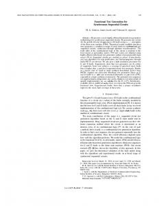
Figure 1. A realization of function z = ac’ + a’c + bc
t1 t3 t5
Table 1.Coupling delay test set
t1 t3 t5 t7 t9 t11
t2 t4 t6 t8 t10 t12
t7 t9 t10 t12 t14
Table 2. Functional delay test with single transition
t1 t3 t5 t7 t11
Robust detection 1 1 1 1 1 0 0 1 1 1 1 1
Output Non-robust detection 0 0 0 0 0 0 0 0 0 0 0 0
t2 t4 t6 t10 t12
Robust detection SIT t2 t4 t6 MIT t8 Non-robust detection t11 t13 t15
Table 5. Detection matrix X for multiple transitions
Inputs
Input a
Let’s generate functional delay test patterns with multiple transitions. The corresponding functional delay test patterns are presented in 0, and the detection matrix X is presented in 0. As we can see, the robust detection includes 9 test patterns, while non-robust detection includes 6 test patterns. The numeration of test patterns has no any relation to 0 or 0. The robust detection was divided in two parts: single input transition and multiple input transitions. This simple example shows that the multiple transitions do not exclude entirely the single transition. In general, the number of test patterns is increased. These test patterns already cover all the paths of the circuit realization. That shows that the generation based on the detection matrix X and multiple transitions is preferable than the generation based on the detection matrix X and single transition. Not all the paths are covered robustly but nevertheless all the
Input b Input c
Robust detection 1 1 1 1 1 0 0 1 1 1 1 1
Output Non-robust detection 1 1 1 1 0 1 1 0 1 1 1 1
4. Test generation In this section, we present a new functional delay test generation algorithm based on the ideas introduced in the previous section. The algorithm (0) has the following input parameters: n – the number of the primary inputs of the circuit; m – the number of the primary outputs of the circuit; L – the number of the randomly generated patterns. The parameter L defines the size of the set from which a pair of test patterns is selected.
262
Generation of Functional Delay Test with Multiple Input Transitions
1. To read the functional delay test from the file and to count the number of test patterns tk. 2. X=||xi,j:=0||2n x 4m; 3. tp:=1; // index of test patterns in the test set 4. DO WHILE (tp≠tk) 5. DO t:=tp, tk, 2; // Filling up the matrix X 6. P1:=Pt; R1:=function(P1); 7. P2:=Pt+1; R2:=function(P2); 8. DO i: =1, n, 1; 9. P3: =P2; 10. d:=1- p1i; 11. IF (p1i≠p2i) THEN 12. p3i:=1- p2i; R3=function(P3); 13. DO j: =1, m, 1; 14. c:=3- r1j; 15. IF (r3j≠r2j) THEN 16. IF(r2j≠r1j) THEN x2i-d,4j-c:=1; 17. ELSE x2i-d,4j-c+2:=1; 18. ENDIF; 19. ENDIF; 20. ENDDO; 21. ENDIF; 22. ENDDO; 23. ENDDO; 24. tp:=tk; h:=tk+1; // index for a new test pattern that has to be included into the test set 25. SKM:=0; // random 2 patterns generation and selection of the best pair from L generated 26. DO k:=1, L, 1; 27. P1:= (p11,p12,...,p1i,...,p1n), p1i:=Random(0,1); R1:=function(P1); 28. P2:= (p21,p22,...,p2i,...,p2n), p2i:=Random(0,1); R2:=function(P2); 29. SK1:=0;SK2:=0; 30. DO i: =1, n, 1; 31. P3: =P2; 32. d:=1- p1i; 33. IF (p1i≠p2i) THEN 34. p3i:=1- p2i; R3=function(P3); 35. DO j: =1, m, 1; 36. c:=3- r1j; 37. IF (r3j≠r2j) THEN 38. IF(r2j≠r1j) THEN 39. IF (x2i-d,4j-c=0) 40. THEN SK1:= SK1+1;ENDIF; 41. ELSE IF (x2i-d,4j-c+2=0) 42. THEN SK2:= SK2+1; ENDIF; 43. ENDIF; 44. ENDIF; 45. ENDDO; 46. ENDIF; 47. ENDDO; 48. IF ((SK1+SK2)>SKM) THEN SKM:=SK1+SK2; P1M:=P1;P2M:=P2; ENDIF; 49. ENDDO; 50. IF (SKM>0) THEN Ph:=P1M; Ph+1:=P2M;h:=h+2; tk:=h; ENDIF; 51. ENDWHILE; Figure 2. Delay test generation algorithm
the calculation when no more pair of patterns is selected from L randomly generated ones. The filling up of the detection matrix X is done according to the input patterns from the set P and their responses R on the outputs. Initially, before the outer loop, the matrix X is filled up with zeros. The responses are calculated for
The algorithm can be divided into three major parts: reading the test patterns from the file (line 1), filling up the detection matrix X (lines 5-23), and random 2 test patterns generation (lines 25-50). The second and the third parts of the algorithm are joined together by the outer loop (line 4), which terminates
263
V. Jusas, K. Motiejūnas Table 6. The parameters of the non-redundant ISCAS’85 benchmark circuits
the pair of input patterns (lines 6 and 7). The loop is repeated for every primary input of the circuit. The value of the input is complemented and assigned to the variable d (line 10). The interest is only for the pair of values which differ. The signal transition is blocked, and the response is calculated (line 12). Next, all the values on the outputs are checked. The interest is only for the values which indicate the difference between the fault-free and the faulty pattern. The control statement in the line 16 indicates what detection is: robust (line 16) or non-robust (line 17). The use of the variables d and c allows writing indices for the matrix entries in the compact form. The third part of the algorithm selects 2 test patterns from 2xL randomly generated ones. The value of L defines the size of randomly generated test set. The 2 best patterns are selected from this set. The best are those ones, which cover the biggest number of the entries of the detection matrix. No difference is made between robust and non-robust test patterns. The part of the algorithm that selects 2 test patterns is similar to the part of the algorithm that fills up the detection matrix X, but it has some extra lines. Firstly, it uses the variables SK1, SK2, SKM for choosing the best pair of test patterns. Next, only unoccupied entries of the matrix are counted for a new generated pair of test patterns (lines 39-42). When the loop that generates L pairs of test patterns is over, if a pair of patterns was selected, then it is copied to the set of test patterns, and the outer loop continues (line 50). If no pair of patterns was selected the algorithm terminates. We will investigate the relation between the quality assessment of the functional test and the transition fault coverage at the gate level in the next section.
Circuit
Gates
Input
Output
n
m
Kmax
No of transition faults
C432
160
36
7
540
1412
C499
202
41
32
5184
3430
C880
383
60
26
1326
2396
C1355
546
41
32
5184
3350
C1908
880
33
25
3004
4848
C2670
1193
157
64
3320
5646
C3540
1669
50
22
2588
8960
C5315
2307
178
123
10540
13816
C6288
2406
32
32
3068
14422
C7552
3512
206
107
12188
19160
Table 7. Robust and non-robust detection
Circuit
Test size
Number of non-zero entries Robust detection
Non-robust detection
%
C432
284
345
345
64
C499
446
907
1258
25
C880
274
606
599
46
C1355
612
1518
1313
29
C1908
632
1001
1027
34
C2670
518
1758
1512
53
5. Experimental results
C3540
806
1672
1664
65
The experiments were carried out on ISCAS85 benchmark circuits. The parameters of circuits are presented in 0. It is worth to pay attention to the fifth column under name “Kmax”. This column shows the highest number of non-zero entries of the detection matrix X for robust detection. These values were taken from 0. They express the quality of the functional test at the functional level. The values for non-robust detection are not known but they can not exceed the given values. To obtain the maximal value Kmax for the functional test according to the software prototype is quite a complex task, because not all the inputs have influence to the outputs, and the impact may propagate trough the even and/or uneven number of the inversions. The determination of the maximal value Kmax of the non-zero entries is complicated in any case, even when the structure of the circuit is known, because the impact of the input can not be propagated along all the paths that connect the input and the outputs. Therefore Kmax for the functional test can be obtained only analytically.
C5315
602
4992
4772
47
C6288
244
2346
2354
77
C7552
922
5236
5087
43
The relationship between the quality assessment of the functional test and the transition fault coverage has to be determined. During the first experiment, the transition fault test that was generated automatically at the gate level by TetraMAX and that has 100% transition fault coverage was taken for the investigation. The value of the criterion that shows the number of non-zero entries of the detection matrix X was calculated for robust and non-robust detection separately (0). The last column of 0 presents the per cent of the number of non-zero entries for robust detection to the maximal value (0, column under name “Kmax”). As we can see, the obtained values are far enough from the maximal value. The maximal value of the non-robust detection is unknown. One can expect that it can not exceed the maximal value of the robust detection but no one can be sure that it always can be reached. The results in 0 show that the obtained value of the non-
264
Generation of Functional Delay Test with Multiple Input Transitions Table 9. Multiple and single transition
robust detection is comparable with the obtained value of the robust detection. On the base of the experiment, we can state that the quality assessment of the test that is generated at the gate level and that detects all the transition faults does not reach the maximal value of the criterion at the functional level. Such a result can be explained by the method of test generation that does not target to generate the test patterns for the sensitization all the paths between the inputs and the outputs. The path is sensitized only from the target fault to the output of the circuit. Meanwhile, the functional delay test targets to propagate the effects of transition faults along all the paths of the circuit. Such an objective allows propagating the effects of transition faults by longer paths.
Circuit
Table 8. The influence of robust and non-robust detection
Circuit
Robust
Non-robust %
Total Num.
%
Num.
C432
74
26
80
28
26
9
C499
220
49
172
38
30
6
C880
56
20
42
15
10
2
C1355
302
49
266
43
92
15
C1908
290
45
276
43
190
30
C2670
120
23
128
24
44
8
C3540
192
23
176
21
66
8
C5315
36
5
20
3
6
1
C6288
4
1
8
3
2
1
C7552
148
16
134
14
50
5
Single transition Test size %
C432
514
96
610
91.22
C499
3888
94.64
10302
99.65
C880
1242
92.61
1920
96.08
C1355
3738
94.33
10292
99.01
C1908
2188
83.56
4612
94.76
C2670
1538
99.17
3584
96.48
C3540
1708
96.90
2954
84.30
C5315
3896
100
9604
98.18
C6288
962
100
2064
99.75
C7552
7920
94.46
11602
96.52
Aver.
2759
95.16
5754
95.59
The functional test has 100% coverage of matrix X at the functional level, except the circuits C2670 and C7552. The circuit C2670 had only 87% coverage of the detection matrix X, meanwhile the transition fault coverage of this circuit is very high (99.17%). The circuit C7552 had 94% coverage of the detection matrix X, and the transition fault coverage of this circuit is almost the same (94.46%). The problem that did not allow achieving the full coverage at the functional level is the large number of primary inputs, and, consequently the large number of combinations of random patterns. The value of parameter L for these circuits was increased till 1000000, but still it did not allow covering the detection matrix fully. The full coverage of transition faults was obtained for the circuits C5315 and C6288. It is a very good result. The results for the columns under name “Single transition” are taken from 0 and included for the comparison purposes. The denomination “Single transition” shows that the patterns in the pair differ only by a single value. As we can see, the size of test, which is based on multiple transitions, is always smaller than the size of test, which is based on single transition. For some circuits, like C499, C1355, C5315, C6288, the size of test is smaller several times. But the transition fault coverage is comparable in both cases. The basic algorithm of test generation can be modified in several ways. Firstly, the random generation can be modified. There is a meaning to make the transitions only on the inputs of the circuit from which the transitions can be propagated along the paths to the outputs of the circuit. Such inputs are usually called active inputs. So, when the second pattern of the pair is generated randomly, the possibility to propagate the transition on every input can be checked, and transitions should be generated only on the active inputs of the circuit. Secondly, the experiments show that pseudorandom test length can be reduced if adjacent patterns are generated 0. So, when the pair of patterns is selected, the adjacent patterns could be
%
Num.
Multiple transition Test size %
In order to determine the influence of the robust and non-robust detection to the selection of the test patterns the second experiment was performed (0). The transition fault test (0) that has 100% transition fault coverage at the gate level was taken for the investigation. The columns of 0 next to the first column are grouped in pairs. The first column of the pair shows the number of the test patterns that were not selected according to the criterion, meanwhile the second column of the pair expresses this value in per cent. As we can see, the per cent of the lost test patterns is quite high when criteria were considered separately. The results are much better when the selection is based on the unified criterion which considers the robust and non-robust detection. The latter result amplifies the value of the non-robust detection. During the third experiment, the functional test was constructed according to the detection matrix X and the obtained test was evaluated at the gate level for transition faults (0).
265
V. Jusas, K. Motiejūnas
test generation based on this relationship emphasizes the higher value of robust test patterns but it acknowledges the fact that non-robust test patterns contribute to transition fault coverage as well. The use in the pair of test patterns with multiple input transitions enables to decrease the size of test set without loss of transition fault coverage.
generated for it. Thirdly, the robust and non-robust detections are evaluated equally in the basic algorithm. The coefficients could be introduced that would provide the different influence for robust and nonrobust detections. The test generation mode of the basic algorithm was modified in two different ways: 1) the second pattern of the pair was generated randomly; the active inputs were identified, and their values were complemented in the first pattern of the pair; 2) firstly, the only robust test was generated, then it was augmented by the non-robust test. The results are presented in 0.
References [1] F. Corno, P. Prinetto, M. Sonza Reorda. Testability analysis and ATPG on behavioral RT-level VHDL. Proceedings of IEEE International. Test Conference, October 1997, 753-759. [2] S. Chiusano, F. Corno, P. Prinetto. A Test Pattern Generation Algorithm Exploiting Behavioral Information. Proceedings of Seventh Asian Test Symposium (ATS'98), Singapore, December 1998, 480-485. [3] E.M. Rudnick, R. Vietti, A. Ellis, F. Corno, P. Prinetto, M. Sonza Reorda. Fast Sequential Circuit Test Generation Using High-Level and Gate-Level Techniques. Proceedings of IEEE Design, Automation and Test in Europe, Feb. 1998, 570-576. [4] F. Ferrandi, F. Fummi, D. Sciuto. Test Generation and Testability Alternatives Exploration of Critical Algorithms for Embedded Applications. IEEE Transactions on Computers, Vol.51, Issue 2, 2002, 200–215. [5] C.H. Cho and J. R. Armstrong. B-algorithm: a Behavioral Test Generation Algorithm. Proceedings of International Test Conference, October 1994, 968– 979. [6] G. Buonanno, F. Ferrandi. L. Ferrandi. F. Fummi, D. Sciuto. How an “Evolving” Fault Model Improves the Behavioral Test Generation. Proceedings of Great Lakes Symposium on VLSI, 1997, 124–130. [7] M. Psarakis, D. Gizopoulos, A. Paschalis. Test generation and fault simulation for cell fault model using stuck-at fault model based test tools. Journal of Electronic Testing, Vol.13, 1998, 315-319. [8] J. Yi, J.P. Hayes. A Fault Model for Function and Delay Testing. Proc. of the IEEE European Test Workshop, ETW'01, 2001, 27-34. [9] J. Yi, J.P. Hayes. The Coupling Model for Function and Delay Faults. Journal of Electronic Testing: Theory and Applications, Vol.21, No.6, 2005, 631–649. [10] H. Kim, J.P. Hayes. Realization-Independent ATPG for Designs with Unimplemented Blocks. IEEE Trans. on CAD, Vol.20, No.2, 2001, 290–306. [11] P. Goel. An Implicit Enumeration Algorithm to Generate Tests for Combinational Logic Circuits. IEEE Trans. on Computers, Vol. C-30, No.3, 1981, 215–222. [12] J. Yi, J.P. Hayes. High-Level Delay Test Generation for Modular Circuits. IEEE Transactions on Computer-Aided Design of Integrated Circuits and Systems, Vol.25, No.3, March 2006, 576-590. [13] E. Bareisa, V. Jusas, K. Motiejunas, R. Seinauskas. The Realization-Independent Testing Based on the Black Box Models. INFORMATICA, Vilnius, Institute of Mathematics and Informatics, Vol.16, No.1, 2005, 19-36.
Table 10. Different generation modes
Circuit
Active inverted Test size %
Robust before Test size %
C432
386
88.81
824
97.75
C499
1814
91.31
5608
100
C880
918
90.65
2116
99.25
C1355
1914
92.33
5622
97.25
C1908
1560
83.93
3944
94.62
C2670
978
90.74
2540
99.42
C3540
1354
88.68
3592
99.03
C5315
2264
97.96
7902
100
C6288
582
98.70
1548
99.97
C7552
3370
94.34
10414
94.88
Aver.
1514
91.75
4411
98.22
The distinguished feature of the first modification was that there was no circuit that would reach the full coverage of detection matrix X. Consequently, the transition fault coverage was lower than in the other two generation modes. The best quality of transition fault coverage was obtained in the third generation mode, when robust test patterns were generated in the beginning of test generation, and then the test patterns were augmented by the non-robust test patterns. Such a result emphasizes the higher value of robust test patterns but it acknowledges the fact that non-robust test patterns contribute to the transition fault coverage as well.
6. Conclusion The functional delay test can be developed in parallel with the other stages of the design and that does not increase the time-to-market. The quality of the functional delay test can be assessed in the initial stages of the design according to the software prototype of the device. The assessment of the quality is based on the relationship of the values on the primary outputs to the values on the primary inputs. The relationship is expressed in two different modes: functional robust and functional non-robust. The delay
266
Generation of Functional Delay Test with Multiple Input Transitions [14] E. Bareiša, V. Jusas, K. Motiejūnas, R. Šeinauskas. Application of Functional Delay Tests for Testing of Transition Faults and Vice Versa. Information Technology And Control, Kaunas, Technologija, 2005, Vol. 34, No.2, 95 - 101. [15] E. Bareiša, V. Jusas, K. Motiejūnas, R. Šeinauskas. Transition Test Supplement. Elektronika ir elektrotechnika = Electronics and electrical engineering. ISSN 1392-1215, Kaunas, Technologija, 2006, No. 3(67), 19–24. [16] E. Bareiša, V. Jusas, K. Motiejūnas, R. Šeinauskas. Functional Delay Test Construction Approaches. Elektronika ir elektrotechnika = Electronics and electrical engineering. ISSN 1392-1215. Kaunas, Technologija, 2007, No. 2(74), 49 - 54. [17] I. Pomeranz, S.M. Reddy. On Testing Delay Faults in Macro-based Combinational Circuits. Proc. Int. Conf. Computer-Aided Dsign, San Jose, CA, 1994, 332-339. [18] F. Ferrandi, F. Fummi, G. Pravadelli, D. Sciuto. Identification of Design Errors Through Functional Testing. IEEE Transactions On Reliability, Vol.52, No.4, December 2003, 400-412.
[19] F. Ferrandi, F. Fummi, D. Sciuto. Implicit Test Generation for Behavioral VHDL Models. Proceedings of International Test Conference, 18-23 October 1998, 587-596. [20] E. Bareiša, V. Jusas, K. Motiejūnas, R. Šeinauskas. Functional Digital Systems Testing. ISBN 9955-25008-9, Kaunas, Technologija, 2006, 281. [21] E. Bareiša, V. Jusas, K. Motiejūnas, R. Šeinauskas, Functional Delay Test Quality Assessment at High Level of Abstraction. Information Technology And Control, Kaunas, Technologija, 2007, Vol.36, No.1, 715. [22] M. Michael, S. Tragoudas. ATPG Tools for Delay Faults at the Functional Level. ACM Transactions on Design Automation of Electronics Systems, Vol.7, No.1, January 2002, 33-57. [23] J. Sosnowski, T.Wabia, T.Bech. Path Delay Fault Testability Analysis. Proceedings of IEEE DFT Int. Symposium on DFT in VLSI Systems, 2000, 338-346. Received June 2007.
267