1344
IEEE TRANSACTIONS ON ELECTRON DEVICES, VOL. 58, NO. 5, MAY 2011
Electron Trapping in HfAlO High-κ Stack for Flash Memory Applications: An Origin of Vth Window Closure During Cycling Operations Xue Feng Zheng, Colin Robinson, Wei Dong Zhang, Jian Fu Zhang, Bogdan Govoreanu, Member, IEEE, and Jan Van Houdt, Senior Member, IEEE
Abstract—Endurance is one of the key criteria for Flash memory technologies, particularly for the generations beyond 30 nm with high-κ materials. It is observed in this paper that the electron trapping in high-κ layers causes threshold-voltage window closure under dynamic program/erase cycling operations. This closure does not originate from the generation of new traps or from further trapping of electrons injected from the gate during erasing. By utilizing a recently developed multipulse technique, it is found that the energy distribution of the electron trapping in the high-κ layer significantly changes after cycling. Electron trapping at the deeper energy levels continuously increases as cycling proceeds, because it does not reach saturation within one programming pulse. The trapping in deep levels cannot be discharged under typical erase conditions, and an increase in deep-level trapping also causes a reduction of trapping at shallow levels. It is concluded that the window closure observed in this paper is caused by a combination of increased deep trapping after erasing and a reduction of shallow trapping after programming. Index Terms—Electron trap, endurance, energy distribution, Flash memory, high-κ dielectrics, pulsed I–V , window closure.
I. I NTRODUCTION
H
IGH-κ materials will soon replace the conventional SiO2 based dielectric stacks as the interpoly/blocking dielectric layers in floating-gate/charge-trapping Flash memory cells for technologies beyond the 30-nm generation [1]–[4]. Recent research has been focused on the improvement of the retention/endurance performance of Flash memory cells using high-κ dielectric stacks, predominantly through energy barrier engineering and dielectric structure optimization [4]–[6]. Few
Manuscript received September 6, 2010; revised November 30, 2010 and January 26, 2011; accepted February 5, 2011. Date of publication March 10, 2011; date of current version April 22, 2011. The test sample used in this work was provided by the Interuniversity Microelectronics Center. The work is supported in part by the Engineering and Physical Sciences Research Council under Grant EP/C508793/2 and in part by the Higher Education Funding Council for England Postgraduate Regularity Framework scheme. The review of this paper was arranged by Editor Y.-H. Shih. X. F. Zheng is with the School of Engineering, Liverpool John Moores University, L3 3AF Liverpool, U.K., and also with the School of Microelectronics, Xidian University, Xi’an 710071, China. C. Robinson, W. D. Zhang, and J. F. Zhang are with the School of Engineering, Liverpool John Moores University, L3 3AF Liverpool, U.K. (e-mail:
[email protected]). B. Govoreanu and J. Van Houdt are with the Technology Units, Process Technology Division, Interuniversity Microelectronics Center, 3001 Leuven, Belgium. Color versions of one or more of the figures in this paper are available online at http://ieeexplore.ieee.org. Digital Object Identifier 10.1109/TED.2011.2115244
attentions, however, have been paid to the effects of the electron trapping/detrapping in the high-κ layer on the endurance performance during the program/erase (P/E) cycling. It is well known that the electron trap density in high-κ materials is several orders of magnitude higher than that in conventional SiO2 [7]. This limits the memory retention due to the excessive low-field leakage current induced by trapassisted tunneling [8]. For the endurance, the threshold-voltage window closure after the erase operation has been observed in Flash memory cells with high-κ layers [5], [9], which has been attributed to the generation of new bulk/interface traps. Although the large amount of electron trapping in the high-κ layer may also affect the memory window stability during the P/E cycling, this has not been investigated in detail yet, mainly due to the limitation of existing measurement techniques in obtaining detailed information on electron traps in thick high-κ layers for the Flash memory application, particularly with regard to their energy and spatial locations. For example, the charge pumping techniques can only reach traps at around 2 nm from the substrate interface [10]–[13], and no information on trapping at energy levels outside the Si band gap can be obtained. The charge injection and sensing (CIS) technique can only probe a limited region above the Si conduction-band edge ECB within 2 ∼ 3 nm into the high-κ bulk. Majority of the traps in the bulk cannot be probed [14]. The traditional CV /IV techniques are too slow to characterize the defects near the interface because of fast detrapping [15], [16]. The single-pulse I–V technique did not give the energy and spatial distributions of defects [17]. We have recently developed a new discharge-based multipulse (DMP) technique [18], which can provide the electron trap energy distribution both above and below Si ECB throughout the SiO2 /high-κ stack. Limitations in techniques such as charge pumping and CIS have been overcome. By using the new DMP technique, electron trapping energy distributions in high-κ materials under dynamic operation conditions similar to that used for the Flash memory P/E cycling are investigated in this paper. It is found that the increase in the electron trapping at deep energy levels in the high-κ layer causes the threshold-voltage window closure. This paper is organized as follows: After a description of the devices and the measurement setup in Section II, the window closure and the electron trapping under cycling conditions are investigated, and the corresponding energy distribution are obtained by using
0018-9383/$26.00 © 2011 IEEE
ZHENG et al.: ELECTRON TRAPPING IN HfAlO HIGH-κ STACK
1345
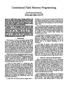
Fig. 1. Illustration of the structures of the floating-gate Flash memory cell and the MOSFET. ttrap is the equivalent distance of electron traps in the high-κ stack to the gate.
the DMP technique in Section III. The causes for the change of the electron trapping energy distribution during the cycling operation are also discussed. II. D EVICES AND E XPERIMENTS In order to gain a direct insight into the electron trapping in the high-κ layer, n-channel metal–oxide–semiconductor fieldeffect transistors (nMOSFETs) with the gate dielectric of a SiO2 /high-κ stack similar to that used in the Flash memory cells are selected in this paper instead of Flash memory devices. This can avoid the complication caused by the coexistence of the electron trapping in both the high-κ dielectric layer and the charge-storing layer in a Flash memory cell. To ensure that the test conditions for the high-κ layer in an nMOSFET match those used in floating-gate Flash memory cells, the parameters of the high-κ layer and the stress conditions are carefully selected to emulate those in the Flash memory cells. The nMOSFETs with polygate were fabricated at the Interuniversity Microelectronics Center, with length and width of 3 and 100 μm, respectively. The high-κ gate stack consists of a 2-nm SiON bottom layer and a 12-nm HfAlO high-κ layer prepared by atomic layer chemical vapor deposition using a process flow similar to that used for forming the dielectric stack in Flash memory devices [19]. Rapid thermal annealing at 900 ◦ C was carried out on all samples for 30 s after the n+-poly deposition. The dielectric constant of the high-κ dielectric is 14. The electron trapping in the high-κ layer will result in the threshold-voltage shift ΔVth in both nMOSFETs and Flash memory devices, as shown in Fig. 1. In both cases, the same high-κ stack is used. If the distance of the electron trapping to the gate ttrap and the electron trapping sheet density Not are the same, the same ΔVth will be induced in both devices according to ΔVth =
Not · q · ttrap εdielectric
(1)
where q is the electron charge and εdielectric is the permittivity of the gate dielectric. Therefore, MOSFETs can be used to study the effects of the electron trapping in the high-κ stack on ΔVth in Flash memory cells if identical stress conditions are applied to the high-κ stack in MOSFETs and Flash memory devices.
The pulsed I–V technique [18], [20] is used to measure the threshold voltage of the device under test. The measurement system consists of an Agilent 81101A pulse generator, a current–voltage converter, and an Agilent DSO6104 oscilloscope. The shift of threshold voltage ΔVth induced by the electron trapping/detrapping is measured at a constant drain current of 1 × 10⁻⁴ A and a drain bias of 100 mV. In order to investigate the electron trapping in the high-κ layer during cycling, a waveform in Fig. 2(a) is applied to the gate repeatedly to emulate the P/E cycling. The first pulse is applied for programming with a peak bias of VP for a period of TP . On the falling edge of this pulse, the threshold voltage after programming Vth,P is measured, as indicated by the arrow. The pulse is then inverted to commence erasing. The peak bias and period of the erasing pulse is VE and TE , respectively. Since the threshold voltage of an nMOSFET is normally larger than 0 V, the threshold voltage after erase Vth,E cannot be measured from the rising edge of this erasing pulse. An additional small measurement pulse is applied following the erasing pulse to measure Vth,E . The width and the rising/falling time of this measurement pulse are 9 and 5 μs, respectively, and its peak level is set to 0.2 V higher than Vth,P , which ensures that the threshold voltage can be measured and the trapping/detrapping during the measurement is suppressed [21]. Vbase of all pulses during this procedure is kept at 0 V. The typical parameters used during the cycling operation are as follows: In a floating-gate Flash memory device with a high-κ interpoly dielectric (IPD) layer, the P/E bias is normally around ±15 V [19], [22], i.e., +15 V for programming and −15 V for erasing. Considering that the coupling ratio is between 0.6 ∼ 0.7, the biases across the IPD layer are around ±5 V. Therefore, in this paper, +5 and −5 V are used as the programming and erasing biases, respectively. Values of 100 μs and 1 ms are used as the typical programming and erasing times, respectively, to comply with the industrial requirements for the Flash memory operation. The DMP technique is used to measure the electron trapping energy distribution during cycling. Under a given Vdischarge , only electron traps with an energy level higher than the silicon conduction-band bottom can be discharged via tunneling [18] since there are little empty states in the silicon band gap. If a gate bias gives the corresponding potential drop of VSiO2 across the SiO2 layer, the energy level of electron traps will change by
1346
IEEE TRANSACTIONS ON ELECTRON DEVICES, VOL. 58, NO. 5, MAY 2011
Fig. 3. Electron trapping energy distributions after programming and erasing on devices with 1 and 10 000 P/E cycles, respectively. ΔEIL is the energy level of electron traps changed in the high-κ layer at the SiO2 /high-κ interface with regard to the Si conduction-band bottom. ΔEIL is equal to the corresponding potential drop across the SiO2 layer, i.e., VSiO2 [18]. The second y-axis shows the equivalent discharged trap sheet density at the substrate/dielectric interface. The second x-axis shows the corresponding trap depth with respect to the conduction-band bottom of the high-κ layer.
Once the discharge reaches saturation, Vg is lowered to another Vdischarge , and the discharging process is repeated until all trapped charges are discharged. Traps being analyzed in this paper are bulk traps in the high-κ dielectric, including those at the interface of the interfacial and high-κ layers. No assumption is made on the spatial distribution of electron traps in the high-κ layer in this paper, and the band bending caused by the trapping in the high-κ layer is not considered in order to simplify the analysis. The detailed parameters used for the DMP technique is given in [18]. III. R ESULTS AND D ISCUSSIONS A. Electron Trapping Before and After Cycling
Fig. 2. (a) Illustration of the typical waveform used for P/E during each P/E cycle. VP and TP are the bias and the time for programming, respectively. VE and TE are the bias and the time for erasing, respectively. Vth,P is the threshold voltage after programming. (b) Energy-band diagram of the SiO2 / high-κ stack during the discharge at a negative gate bias. If a gate bias gives the corresponding potential drop of VSiO2 across the SiO2 layer, the energy level of electron traps will change by ΔEIL = qVSiO2 in the high-κ layer at the SiO2 /high-κ interface and by ΔEG = qVdielectric at the high-κ/gate interface. Vdielectric is the potential drop across the SiO2 /high-κ stack. (c) ΔVth after program and erase during cycling. The bias for programming is 5 V for 100 μs. The bias for erasing is −5 V for 1 ms.
ΔEIL = qVSiO2 in the high-κ layer at the SiO2 /high-κ interface and by ΔEG = qVdielectric at the gate interface, as illustrated in Fig. 2(b). The traps within the energy range of ΔEIL and ΔEG become dischargeable. The energy spectroscopy of electron traps can be therefore measured by sweeping the gate bias, and ΔEIL can be used as an indicator for the energy range. Once the cycling operation completed, the gate bias is lowered to the discharge bias Vdischarge for discharging.
The shifts of the threshold voltage ΔVth after program and erase during cycling are shown in Fig. 2(c). A clear ΔVth window closure is observed. ΔVth after erase significantly increases during cycling, whereas ΔVth after program increases only slightly. It is noted that the window closure after the erase operation has been also observed during the endurance cycling test in Flash memory cells with a high-κ layer [9], [23]. The increase in ΔVth in Fig. 2(c) clearly shows that the electron trapping in the high-κ layer accumulates after the erase operations, which results in the window closure. In order to understand the reason for the accumulation of the trapping after erase, the electron trapping energy distribution during cycling is measured by using the DMP technique. The total threshold-voltage shift under each discharging bias during the DMP technique is measured and plotted against the corresponding trap energy level ΔEIL . The results after 1 and 10 000 P/E cycles are compared in Fig. 3, including the distributions both after program and erase. After the first program pulse, the energy distributions in the high-κ layer is dominated by the electron trapping at the energy levels above the Si conduction-band ECB bottom, which agrees well with our
ZHENG et al.: ELECTRON TRAPPING IN HfAlO HIGH-κ STACK
1347
previous results [18]. Following the first erase pulse, most electron trapping processes are discharged. After 10 000 cycles, the electron trapping at the deep energy levels significantly increases after both the program and erase pulses, indicating that the deep electron trapping increases with cycling and cannot be erased by the erase pulse. For the shallow traps, there is no significant change after erase when compared with that after the first erase pulse, indicating that all shallow traps can be discharged after cycling. Therefore, the increase in ΔVth after erase on the cycled device shown in Fig. 2(c) can be only caused by the increased trapping at deep energy levels that cannot be erased. It is also observed that the trapping at shallow energy levels significantly decreases after program on the cycled device when compared with that after the first program pulse. The reason for the increase in the deep trapping and the decrease in the shallow trapping after cycling will be investigated in the succeeding sections. B. Energy Distribution of the Electron Trapping During Cycling Three possible reasons for the increase in the deep trapping during cycling are examined here: an increase in the trapping by generating new traps during cycling; an electron injection from the gate during erasing; and the nonsaturation of the trapping at deep levels during programming. 1) Generation of New Traps During Cycling: To explore the possibility whether the increased deep electron trapping are caused by new traps generated during cycling, these deep traps are discharged and then refilled under the typical program condition. If new traps are generated, they should lead to higher trapping during refilling when compared with the trapping before cycling. A comparison between the refilled trapping distribution and that after the first program pulse on a fresh device will reveal if there is any new deep trap generation therefore. Fig. 4(a) shows that, although the deep trapping can survive the normal erasing under Vg = −5 V, an application of Vg = −7 V leads to full discharging. In fact, ΔVth becomes negative at longer time, indicating that positive charges are formed at −7 V. Therefore, the discharge on the cycled device under Vg = −7 V is caused by both the electron detrapping and the recombination of holes with the trapped electrons. After the discharge, the cycled device was programmed again at 5 V for 100 μs. The DMP technique was then carried out to evaluate the electron trapping distribution. Fig. 4(b) compares the trapping distribution of a fresh device with that of the refilled cycled device after 10 000 cycles. The absence of the deep peak after the discharge at Vg = −7 V suggests that the deep trapping accumulated through the 10 000 cycles can be indeed discharged. The good agreement between the refilling and the trapping on a fresh device allows us to conclude that new traps are not generated in the high-κ stack during cycling. 2) Filling by Electrons Injected From the Gate During Erase: During erase, Vg < 0 is applied, and electrons can be injected from the gate, then tunneling through the high-κ dielectric. These injected electrons may have a chance to be captured, resulting in an accumulation of the electron trapping during the cycling and the window closure.
Fig. 4. (a) Effects of the discharge at −7 V on the cycled device. Positive charges are generated in the gate dielectrics during the discharge of −7 V. (b) After discharging at −7 V on the 10 000-P/E-cycled device, the trap energy distribution after programming recovers and becomes very close to that on the fresh device.
To evaluate this possibility, cycling with only the erase pulses is carried out by using the pulse waveform given in Fig. 5(a). Here, the program pulse is replaced by a small pulse with an amplitude of 1 V and a pulsewidth of 9 μs. This ensures that the electron injection during the program operation is negligible. In Fig. 5(b), ΔVth after the erase pulses during cycling with and without the program pulses are compared. It is clear that ΔVth after erase is negligible without programming. We conclude that the gate injection during erase contributes little to the observed electron trapping and, in turn, the cycling-induced window closure. 3) Nonsaturated Trapping at Deep Levels During Programming: Now, we will examine the third possible reason for the increase in the deep trapping. The width of the program pulse is only 100 μs, during which the electron trapping in the high-κ layer may not reach saturation. During cycling, electrons are repeatedly injected into the high-κ layer by each programming pulse, and the deep trapping may accumulate and cause the window closure if they are not discharged by the erase pulses. The nonsaturation of the trapping during programming is demonstrated in Fig. 6(a), in which the trapping level is
1348
IEEE TRANSACTIONS ON ELECTRON DEVICES, VOL. 58, NO. 5, MAY 2011
Fig. 5. (a) A typical waveform used to evaluate the effect of the erasing operation during the P/E cycling. The program pulse is replaced by a small pulse of 1 V for 9 μs. The erasing bias is −5 V for 1 ms. Vth,P is the threshold voltage measured by the 1-V pulse. (b) The effect of the erasing bias on ΔVth with/without program during P/E cycling.
shown against the program time under the gate bias of 5 V. The trapping at 100 μs, clearly, does not reach saturation. In order to further support that the increase in the electron trapping at deep energy levels during cycling is caused by the continuous trapping, electron trapping energy distributions at various program times of 100 μs, 100 ms, and 10 and 1000 s are compared in Fig. 6(b). The electron trapping at the deep energy levels indeed increases with the program time and does not saturate for up to 1000 s. The trapping at shallow levels will be addressed in the next section. For the device cycled under typical operation conditions, the electron trapping energy distribution after programming for 10 000 cycles is measured and compared with that after continuously programming for 1 s; in both cases, the total program time is 1 s. As shown in Fig. 7, the electron trapping at deeper energy levels in the cycled device is even higher than that in the continuously programmed device, which indicates that the nonsaturation-induced deep trapping is more significant under cycling conditions. This can be explained as follows: It is well known that the electron trapping in the gate dielectric will reduce the gate current significantly under a constant gate bias. Since shallow electron traps are repeatedly discharged by the next erase pulse during cycling, while these traps remain charged during continuous programming, a larger programming gate current in the cycled device is expected. Therefore, the effective electron injection level is higher in the cycled device, which leads to the higher deep trapping level. We can therefore conclude that the increase in the deep trapping in the cycled device is caused by the accumulated deep
Fig. 6. (a) Trapping level versus charging time when the gate is biased at 5 V. (b) Electron trapping energy distribution after charging at 5 V for 100 μs, 100 ms, and 10 and 1000 s, respectively. The electron trapping at the highest energy level initially increases from 100 μs to 10 s and decreases when the charge time further increases to 1000 s. The electron trapping at deep energy levels keeps increasing with the charging time.
Fig. 7. Comparison of electron trapping energy distributions on devices programmed after 1 cycle, 10 000 cycles, and continuously for 1 s The program bias is 5 V.
ZHENG et al.: ELECTRON TRAPPING IN HfAlO HIGH-κ STACK
Fig. 8. Illustration of the energy-band diagram of the HfAlO stack without and with the electron trapping during programming. The electron trapping in HfAlO reduces the effective voltage drop across the interface layer by ΔVSiO2 so that shallower traps in the white region cannot be filled at the end of charging.
trapping during programming, which cannot be discharged by the erase pulse at −5 V. 4) Trapping at Shallow Energy Levels During Cycling: As shown in Fig. 6(b), the electron trapping at a shallow energy level initially increases when the program time increases from 100 μs to 10 s and decreases when the program time further increases to 1000 s. This can be explained by the change of the internal electric field across the high-κ stack caused by the electron trapping. As shown in Fig. 8, during programming under the positive gate bias, the voltage drop across the interfacial layer decreases when the electron trapping in the high-κ layer builds up, due to the reduction of the internal electric field near the interfacial layer. It also raises the trap energy level against the Si ECB so that the shallow traps in the white triangle region of the high-κ layer in Fig. 8 can be no longer filled, leading to the decreased trapping at the shallow energy levels. In order to support this explanation, we increased the program bias from 5 to 5.8 V after 10 000 cycles. Fig. 9 shows that an increase in the program bias indeed raises the electron trapping at shallow energy levels. Therefore, the decrease in the electron trapping at the shallow energy levels is caused by the reduction of the internal electric field across the interfacial layer, which, in turn, is caused by the increase in the deep trapping during cycling. IV. C ONCLUSION The recently developed DMP technique has been used to examine the origin of the window closure with the high-κ layer after the cycling operation. The generation of new traps and the electron injection from the gate during erasing have been ruled out as the reasons. It has been found that the electron trapping located at deeper energy levels continuously increases with cycling but that at the shallower energy levels actually decreases. The increase in the deep trapping is attributed to the nonsaturation in the trapping during each programming step and its ability to survive the erasing step under typical P/E cycling conditions. An accumulation of the deep trapping in the high-κ layer also reduces the potential drop over the interfacial
1349
Fig. 9. Electron trapping energy distribution on the 10 000-cycled device. A program pulse of 5.8 V for 100 μs is applied to compensate the energy level lowering induced by the residual electron trapping in the gate dielectric. It is also compared with the trapping energy distribution after programming at 5 V for 100 μs on a fresh and 10 000-cycled device. During P/E cycling, the programming bias is 5 V for 100 μs, and the erasing bias is −5 V for 1 ms.
layer, which, in turn, results in a reduction of the shallow trapping. We conclude that the window closure originates from the combined effect of the buildup of the deep trapping after erasing and a reduction of the shallow trapping after programming. R EFERENCES [1] J. Van Houdt, “High-κ materials for non-volatile memory applications,” in Proc. IRPS, 2005, pp. 234–239. [2] International Technology Roadmap for Semiconductors, San Jose, CA, 2009. [Online]. Available: http://public.itrs.net [3] B. Govoreanu, D. P. Brunco, and J. Van Houdt, “Scaling down the interpoly dielectric for next generation Flash memory: Challenges and opportunities,” Solid State Electron., vol. 49, no. 11, pp. 1841–1848, Nov. 2005. [4] K. Kim and G. Jeong, “Memory technologies for sub-40 nm node,” in IEDM Tech. Dig., 2007, pp. 27–30. [5] S. Choi, S. J. Baik, and J. T. Moon, “Band engineered charge trap NAND Flash with sub-40 nm process technologies,” in IEDM Tech. Dig., 2008, pp. 925–928. [6] B. Govoreanu, P. Blomme, M. Rosmeulen, J. Van Houdt, and K. De Meyer, “VARIOT: A novel multilayer tunnel barrier concept, for low-voltage nonvolatile memory devices,” IEEE Electron Device Lett., vol. 24, no. 2, pp. 99–101, Feb. 2003. [7] M. Houssa, L. Pantisano, L.-A. Ragnarsson, R. Degraeve, T. Schram, G. Pourtois, S. De Gendt, G. Groeseneken, and M. M. Heyns, “Electrical properties of high-k gate dielectrics: Challenges, current issues, and possible solutions,” Mater. Sci. Eng. R, vol. 51, no. 4–6, pp. 37–85, Apr. 2006. [8] B. Govoreanu, R. Degraeve, J. Van Houdt, and M. Jurczak, “Statistical investigation of the floating gate memory cell leakage through high-κ interpoly dielectrics and its impact on scalability and reliability,” in IEDM Tech. Dig., 2008, pp. 1–4. [9] G. Van den Bosch, L. Breuil, A. Cassiato, A. Rothschild, M. Jurczak, and J. Van Houdt, “Investigation of window instability in program/erase cycling of TANOS NAND Flash memory,” in Proc. IEEE Int. Memory Workshop, 2009, pp. 84–85. [10] I. Crupi, R. Degraeve, B. Govoreanu, D. P. Brunco, P. J. Roussel, and J. Van Houdt, “Energy and spatial distribution of traps in SiO2 /Al2 O3 nMOSFETs,” IEEE Trans. Device Mater. Rel., vol. 6, no. 4, pp. 509–516, Dec. 2006. [11] M. B. Zahid, R. Degraeve, L. Pantisano, J. F. Zhang, and G. Groeseneken, “Defects generation in SiO2 /HfO2 studied with variable T-charge-Tdischarge charge pumping VT2 CP,” in Proc. IEEE Int. Rel. Phys. Symp., 2007, pp. 55–60. [12] E. Cartier, B. P. Linder, V. Narayanan, and V. K. Paruchuri, “Fundamental understanding and optimization of PBT1 in nFETs with SiO2 /HfO2 gate stack,” in IEDM Tech. Dig., 2006, pp. 57–60.
1350
IEEE TRANSACTIONS ON ELECTRON DEVICES, VOL. 58, NO. 5, MAY 2011
[13] Y. Wang, V. Lee, and K. P. Cheung, “Frequency dependent charge-pumping, how deep does it probe?” IEDM Tech. Dig., 2006, pp. 491–494. [14] R. Degraeve, M. Cho, B. Govoreanu, B. Kaczer, M. B. Zahid, J. Van Houdt, M. Jurczak, and G. Groeseneken, “Trap Spectroscopy by Charge Injection and Sensing (TSCIS): A quantitative electrical technique for studying defects in dielectric stacks,” in IEDM Tech. Dig., 2008, pp. 1–4. [15] J. F. Zhang, S. Taylor, and W. Eccleston, “A comparative-study of the electron trapping and thermal detrapping in SiO2 prepared by plasma and thermal oxidation,” J. Appl. Phys., vol. 72, no. 4, pp. 1429–1435, Aug. 1992. [16] W. D. Zhang, J. F. Zhang, R. Degraeve, and G. Groeseneken, “Two types of neutral electron traps generated in the gate silicon dioxide,” IEEE Trans. Electron Devices, vol. 49, no. 11, pp. 1868–1875, Nov. 2002. [17] J. F. Zhang, C. Z. Zhao, M. B. Zahid, G. Groeseneken, R. Degraeve, and S. De Gendt, “An assessment of the location of as-grown electron traps in HfO2 /HiSiO stacks,” IEEE Electron Device Lett., vol. 27, no. 10, pp. 817–820, Oct. 2006. [18] X. F. Zheng, W. D. Zhang, B. Govoreanu, J. F. Zhang, and J. Van Houdt, “A new multi-pulse technique for probing electron trap energy distribution in high-κ materials for Flash memory application,” IEEE Trans. Electron Devices, vol. 57, no. 10, pp. 2484–2492, Oct. 2010. [19] B. Govoreanu, D. Wellekens, L. Haspeslagh, D. P. Brunco, J. De Vos, D. Ruiz Aguado, P. Blomme, K. van der Zandem, and J. Van Houdt, “Performance and reliability of HfAlOx -based interpoly dielectrics for floating-gate Flash memory,” Solid State Electron., vol. 52, no. 4, pp. 557– 563, Apr. 2008. [20] C. Z. Zhao, J. F. Zhang, M. B. Zahid, B. Govoreanu, G. Groeseneken, and S. De Gendt, “Determination of capture cross sections for as-grown electron traps in HfO2 /HfSiO stacks,” J. Appl. Phys., vol. 100, no. 9, p. 093716, Nov. 2006. [21] X. F. Zheng, W. D. Zhang, B. Govoreanu, D. Ruiz Aguado, and J. F. Zhang, “Energy and spatial distribution of electron traps throughout SiO2 /Al2 O3 stacks as the IPD in Flash memory application,” IEEE Trans. Electron Devices, vol. 57, no. 1, pp. 288–296, Jan. 2010. [22] B. Govoreanu, R. Degraeve, M. B. Zahid, L. Nyns, M. Cho, B. Kaczer, M. Jurczak, J. A. Kittl, and J. Van Houdt, “Understanding the potential and limitations of HfAlO as interpoly dielectric in floating-gate Flash memory,” Microelectron. Eng., vol. 86, no. 7–9, pp. 1807–1811, Jul.–Sep. 2009. [23] S. H. Lin, H. J. Yang, W. B. Chen, F. S. Yeh, S. P. McAlister, and A. Chin, “Improving the retention and endurance characteristics of charge-trapping memory by using double quantum barriers,” IEEE Trans. Electron Devices, vol. 55, no. 7, pp. 1708–1713, Jul. 2008.
Xue Feng Zheng received the B.Eng. and M.Sc. degrees in microelectronics and solid-state electronics from Xidian University, Xi’an, China, in 2001 and 2004, respectively, and the Ph.D. degree in microelectronics from Liverpool John Moores University, Liverpool, U.K., in 2010. In 2003, he joined the School of Microelectronics, Xidian University, where he has been an Assistant Professor since 2010. His research interests include the reliability of metal–oxide–semiconductor fieldeffect transistors and the degradation and defect characterization of high-k gate stacks in Flash memory devices.
Colin Robinson received the B.Sc. degree in broadcast engineering from Liverpool John Moores University, Liverpool, U.K., in 2008. Since 2008, he has been with the Microelectronics research group of Liverpool John Moores University. He has over 20 years of worldwide industrial experience gained with companies such as Mars Confectionery and Shell U.K. His current research interests are focused on the characterization of high-k materials for next generations of Flash memory devices.
Wei Dong Zhang received the B.Eng. degree in semiconductor physics and devices from Beijing Institute of Technology, Beijing, China, in 1989, the M.Sc. degree in semiconductor devices and microelectronics from Xidian University, Xi’an, China, in 1992, and the Ph.D. degree in microelectronics from Liverpool John Moores University, Liverpool, U.K., in 2003. From 1992 to 1999, he was a Lecturer and then an Associated Professor with the Institute of Microelectronics, Xidian University. In 2002, he was a Lecturer in microelectronics with Bournemouth University, Bournemouth, U.K. In 2005, he was a Senior Lecturer in microelectronics with Liverpool John Moores University, where he has been a Reader in microelectronics since 2010. He has authored or coauthored over 20 journal and conference papers. His current research interests cover the areas of quality and reliability assessment of complementary metal–oxide–semiconductor and Flash memory devices.
Jian Fu Zhang received the B.Eng. degree in electrical engineering from Xi’an Jiaotong University, Xi’an, China, in 1982 and the Ph.D. degree in electrical engineering from Liverpool University, Liverpool, U.K., in 1987. From 1986 to 1992, he was a Senior Research Assistant with the University of Liverpool, where he worked on the dielectric recovery of plasma in accelerating gas flow, the plasma processing of semiconductors, and the reliability of metal–oxide– semiconductor (MOS) devices. In 1992, he was a Senior Lecturer with Liverpool John Moores University, Liverpool, U.K., where he became a Reader in microelectronics in 1996 and a Professor in 2001. He has authored or coauthored over 100 journal and conference papers, including ten invited papers at several international conferences. His current research interests include performance, degradation, and defect characterization of MOS devices and high-k layers. Dr. Zhang was a member of the technical program committee for the IEEE Semiconductor Interface Specialists Conference.
Bogdan Govoreanu (M’05) received the Lic.Eng. and M.Sc. degrees in electronics from the Technical University of Bucharest (TU Bucharest), Romania, in 1995 and 1996, respectively, and the Ph.D. degree in applied sciences from the Katholieke Universiteit Leuven, Leuven, Belgium, in 2004, for his research carried out at the Interuniversity Microelectronics Center (IMEC), Leuven, Belgium on novel nonvolatile-memory device concepts. In 1996, he was a Research Assistant with the Electronics Department, TU Bucharest. He is currently with the IMEC, where he has been working on various research areas, including modeling, characterization, and reliability of nonvolatile/Flash memory devices, high-k dielectrics, and technology computer aided design methodologies for empirical model building and optimization techniques. He has published over 60 research papers in internationally recognized journals and conference proceedings, and has filed several European and U.S. patent applications. His current research focus is on emerging resistance-switching-based memory concepts.
ZHENG et al.: ELECTRON TRAPPING IN HfAlO HIGH-κ STACK
Jan Van Houdt (SM’02) was born in Leuven, Belgium, on June 20, 1963. He received the M.Sc. degree in electrical and mechanical engineering and the Ph.D. degree in applied sciences from the Katholieke Universiteit Leuven, Leuven, in 1987 and 1994, respectively. His M.S. thesis dealt with the degradation of short-channel metal–oxide– semiconductor (MOS) transistors under hot-carrier injection conditions. His Ph.D. work concentrated on the physics and the characteristics of high-injection MOS (HIMOS) Flash memory devices. After his M.S. thesis, he joined the Interuniversity Microelectronics Center (IMEC), Leuven. In 1990, he invented the HIMOS transistor, which is a novel fast-programmable Flash electrically erasable programmable read-only memory cell that has led to a high-performance cost-effective nonvolatile-memory technology, on which he is the holder of numerous international patents. In 1996, he became responsible for the development and the dissemination of Flash memory technology based on the IMEC’s proprietary concepts, including the licensing and the transfer of these technologies toward four industrial product lines. Since 1999, he has been managing the memory group at the IMEC. From 2000 until 2008, he also managed the IMEC’s Industrial Affiliation Program on Advanced Memory Technology and expanded it to become one of the IMEC’s largest research programs today. His research interests are the physics
1351
of semiconductor devices, hot-carrier injection, and degradation phenomena in MOS structures, thin dielectrics, modeling and optimization of floating gate and nitride nonvolatile memory devices, reliability physics and design aspects of memory devices in general, the application of high-k materials in novel memory devices, as well as emerging nonvolatile memory concepts such as resistance random-access memory. He has published more than 160 papers in international journals, wrote two book chapters, and accumulated more than 140 conference contributions (including more than 20 invitations and four best paper awards). He has filed about 45 patent applications worldwide in the area of nonvolatile-memory devices, out of which 24 patents have been granted so far. Dr. Van Houdt received the Best Student Paper Award at the 22nd European Solid-State Device Research Conference (ESSDERC) in 1992 and the Scientific Award of the Royal Academy for Science, Literature, and Fine Arts of Belgium in 1995. He serves (or served) on the program and/or organizational committees of the IEEE Nonvolatile Semiconductor Memory Workshop; the IEEE Reliability Physics Symposium; the ESSDERC; the International Conference on Memory Technology and Design (ICMTD); the IEEE International Workshop on Memory Technology, Design, and Testing (Taiwan); the Solid-State Devices and Materials conference; the Materials Research Society symposium on nonvolatile-memory technologies; and the IEEE International Electron Devices Meeting. In 2007, he was the General Chairman of the ICMTD.