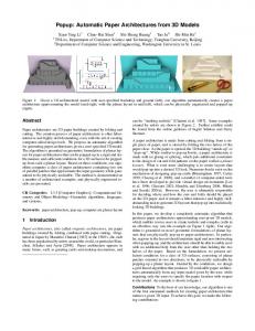
NoC architectures is that the 3 layer fabrication will be simpler compared to 3D .... Figuer 3: c) Dead Space for 2-D and 3-D implementations of ami49. 8.
www.ijird.com
May, 2013
Vol 2 Issue 5
ISSN: 2278 – 0211 (Online)
Evaluation Of 3D Network-On-Chip Architectures By Using Layers Dr.T.Gnanaskaran Professor & HEAD,Department of IT, RMK Engineering College & Technology,Chennai, India P.Kalyanasundaram Associate Professor, Department of ECE, Nandha Engineering college, Erode, India Dinesh kumar PG Scholar, Department of ECE, Nandha Engineering college, Erode, India Abstract: SoC are widely used in high volume and high end application . Due to the exponential growth of the transistor the 2D chip fabrication technology is facing a lot of challenges. The NoC concept replaces design-specific global on chip wires with a generic on-chip interconnection network realized by specialized routers that connect generic processing elements . The architectural level, Networks on- Chip (NoC) has been proposed to address the complexity of interconnecting an ever-growing number of Intellectual Property (IP) blocks like DSP, Memories, I/O Ports, and Peripherals . 3D NoC is a promising choice for implementing scalable interconnection architectures. A design methodology that integrates floor planning where the IP blocks are implemented, routers assignment, and cycle-accurate NoC simulation is proposed to evaluate the performance of the 3D NoC. Let us consider 3D NoC where IP blocks are implemented in top and bottom layers and 3D NoC routers are implemented in the middle layer using mesh topology. The implementation of the 3D NoC routers on a separate layer offers an additional area that may be utilized to improve the network performance by increasing the number of virtual channels, buffers size, and mesh size. The scalability and predictability of NoCs enable designers to design increasingly complex systems, with large numbers of IP/cores and lower communication latencies for many applications. Experimental results show that increasing the number of virtual channels rather than the buffers size has a higher impact on network performance. Increasing the mesh size can significantly improve the network. The 3-layer architecture can offer significantly better network performance compared to the 2D architecture. Key words: 3D NoC, 3D topology, TSVs, IP blocks, traffic rate, buffer size, network diameter. INTERNATIONAL JOURNAL OF INNOVATIVE RESEARCH & DEVELOPMENT
Page 557
www.ijird.com
May, 2013
Vol 2 Issue 5
1. Introduction The integrated circuits contain several processor cores, memory blocks, hardware cores and analog components integrated on the same chip. Such SoC are widely used in high volume and high-end application fields. As the number of cores integrated on a SoC increases with technology scaling parameters, the 2-D chip fabrication technology is facing lot of challenges in utilizing the exponentially growing number of transistors. the number of transistors and the die size of the chip increase, the length of the interconnection links also increases. the performance of the transistors have increased dramatically. However, the performance improvement of interconnection links has not kept places with that of the transistors. With reducing geometries, the wire pitch and cross section area also reduce, thereby increasing the RC components delay of the wires. This coupled with increasing interconnect length leads to long timing delays on global routing wires. The NoC concept replaces design-specific global on chip wires with a generic on-chip interconnection network realized by specialized routers that connect generic processing elements (PE)-such as processors, ASICs, FPGAs, memory. The benefits of the NoC based SoC-design include scalability, predictability, and higher bandwidth [3]. In such scenarios, where flexibility and predictability are primary concerns, homogeneous regular networks are preferred. The NoC topologies have limitations in that communication locality is poorly supported, the utilization of network resources is low. Designs with IP/cores with different sizes are not well suited to implementations based on regular mesh NoC topologies. Therefore, when area and performance are more important .However, the design of these networks is more difficult and specialized routing algorithms are necessary to prevent deadlock [5].
2. Methodology We propose novel 3D NoC architectures and implement an automated designing tool. Our main procedures can be summarized here.
INTERNATIONAL JOURNAL OF INNOVATIVE RESEARCH & DEVELOPMENT
Page 558
www.ijird.com
May, 2013
Vol 2 Issue 5
Figuer 1: a) 2-D IC–2-D NoC. (b) 2-D IC–3-D NoC. (c) 3-D IC–2-D NoC. (d) 3D IC–3-D NoC.
We propose and study two 3D NoC architectures (Two- layer and Three-layer architectures) the homogeneous network on a separate layer and heterogeneous floorplans on different layers. In the network regularity is maintained for flexibility and delay predictability while the IP/cores can have arbitrary sizes. This approach used to avoids design difficulties [15].
For the 2-layer architecture, we propose the use of a floorplanning and routers assignment-based design methodology for the placement of IP/cores on the first layer and the minimization of their connections to the NoC routers located on the second layer. In the case of the 3-layer architecture, the design methodology also includes a partitioning step. The second layer has an additional available area that may be utilized to increase the number of routers or their complexity (e.g., increase the number of virtual channels and the buffers size). In addition, network interfaces (NIs), which are important components of NoC-based systems, also may be placed on the second layer [9].
We implemented a versatile software framework to investigate the benefits of the proposed 3D architectures. Preliminary results on the 2-layer NoC architecture were reported in [11]. We also propose the second 3-layer NoC architecture reducing the footprint area of the chip and at improving the average flit latency.
3. 2-D And 3-D Architectures The 2-layer architecture has two device layers. The first layer is used entirely for the heterogeneous irregular IP/cores, while the second layer is dedicated to the homogeneous regular NoC (Figure 2(b)). This approach simplifies the design process in that it separates the floorplanning optimization from the network topology synthesis. The goal INTERNATIONAL JOURNAL OF INNOVATIVE RESEARCH & DEVELOPMENT
Page 559
www.ijird.com
May, 2013
Vol 2 Issue 5
of the floorplanning step is to find the best floor plan with minimal white space. The second device layer accommodates the regular mesh network. In this way, the network regularity is maintained for flexibility and delay predictability, while the IP/cores can have arbitrary sizes. In addition, a simple packet routing algorithm can be used. The second layer is again dedicated to implementing the NoC, while layers 1 and 3 are used for IP/cores placement (Figure 2(c)).
d) 2D
c) 3-layer architecture
Figure 2(a): Initial floor plan with no routers. (b) 2-layer architecture. (c) 3-layer architecture. (d) 2D This architecture aims to reducing the footprint area of the chip, which in turn leads to shorter physical links, hence improving the network performance. In both proposed architectures, the vertical connections between IP/cores and their assigned routers are realized using through silicon vias (TSV). Routers connected to IP/cores have five ports, while the rest of the routers have only four ports. One advantage of the proposed 3D NoC architectures is that the 3 layer fabrication will be simpler compared to 3D architectures with more than three layers [17], as the misalignment is only between two or three layers. The additional area may be utilized to implement fault/error tolerance techniques such as error correcting codes. To increase the bandwidth of physical links and therefore improve the overall network performance. Alternatively, the extra area also may be utilized to implement thermal monitoring and management schemes [7].
4. Routers Assignment In this step, each floor plan from the list of best M floorplan undergoes the routers assignment step. The regular M × M mesh NoC is constructed on layer 2. This square regular mesh network utilizes the minimum number of routers that can guarantee at least one router for each IP/core. This topology is referred to as the direct topology. However, INTERNATIONAL JOURNAL OF INNOVATIVE RESEARCH & DEVELOPMENT
Page 560
www.ijird.com
May, 2013
Vol 2 Issue 5
the mesh can optionally be expanded to a larger number of routers in both x, y direction in the routers assign.
Figure 2: a) Floorplanning and routers assignment for ami49 using the 2-layer architecture
Figure 2 : b) Floorplanning and routers assignment for ami49 using the 3-layer architecture. The goal of the routers assignment step is to associate each IP/core with a router from the regular mesh on layer 2 such that the total wire length of the extra-links between each IP/core and its assigned router is minimized. This is a linear assignment problem solved by using the efficient algorithm [13]. The algorithm utilizes a bipartite graph with two sets of nodes: left nodes representing the application IP/cores and right-nodes representing the routers of the regular mesh NoC. Edges connect each node from one set to all nodes in the other set. Edge weights are proportional to the Manhattan distance between the IP/core and routers. In this way, we treat the assignment of all IP/cores simultaneously and achieve an overall minimal total length of the extra-links. This step is the same for both 2-layer and 3-layer architectures. The examples from Fig: 2(a, b) also show the result of the routers assignment step.
INTERNATIONAL JOURNAL OF INNOVATIVE RESEARCH & DEVELOPMENT
Page 561
www.ijird.com
May, 2013
Vol 2 Issue 5
5.HMETIS Algorithms The METIS is an algorithm package for partitioning large irregular graphs, partitioning large meshes, and computing of sparse matrices. The METIS provides two stand-alone programs, pmetis and kmetis, to partition graphs into partitions of equal size. The hMETIS algorithms are based on multilevel graph partitioning pmetis is based on multilevel recursive bisectioning described in [10] and kmetis is based on multilevel kway partitioning described in [8]. Multilevel partitioning algorithms are reducing the size of the graph by coarsening the graph's details. This takes form as collapsing adjacent vertices and edges. As the partitioning algorithms operate with the reduced-size graph, they are extremely fast compared to traditional partitioning algorithms that compute a partition directly on the original graph. Extensive testing has also shown that the partitions provided by hMETIS are consistently better than those produced by spectral partitioning algorithms [9]. 00031 void HMETIS_PartRecursive(int nvtxs,
/* [in] nb vertices */
00032
int nhedges,
/* [in] nb hyperedges */
00033
int* vwgts,
/* [in] array vertex weights */
00034
int* eptr,
/* [in] array of indirection on eind (of size
nhedges+1) */ 00035
int* eind,
/* [in] array with all consecutive hyperedges
00036
int* hewgts,
/* [in] array hyperedge weights */
00037
int nparts,
00038
int ubfactor, /* [in] unbalanced factor */
(as vertex set) */
00039
/* [in] nb of desired partitions */
int* options, /* [in] array of 9 integers (options[0]=0 for
default options) */ 00040
int* part,
/* [out] array of computed partitions (of size
nvtxs) */ 00041
int* edgecut); /* [out] nb hyperedges cut */
00042 00043 void HMETIS_PartKway(int nvtxs,
/* [in] nb vertices */
00044
int nhedges,
/* [in] nb hyperedges */
00045
int* vwgts,
/* [in] array vertex weights */
00046
int* eptr,
/* [in] array of indirection on eind (of size
nhedges+1) */ INTERNATIONAL JOURNAL OF INNOVATIVE RESEARCH & DEVELOPMENT
Page 562
www.ijird.com 00047
May, 2013 int* eind,
Vol 2 Issue 5
/* [in] array with all consecutive hyperedges (as
vertex set) */ 00048
int* hewgts,
00049
int nparts,
00050
int ubfactor, /* [in] unbalanced factor */
00051
/* [in] array hyperedge weights */ /* [in] nb of desired partitions */
int* options, /* [in] array of 9 integers (options[0]=0 for
default options) */ 00052
int* part,
/* [out] array of computed partitions (of size
nvtxs) */ 00053
int* edgecut); /* [out] nb hyperedges cut */
00054 00055 00056 #ifdef __cplusplus 00057 } 00058 #endif 00059 00060 #endif
6. NOC Simulation In the last step, each of the best M NoC topologies is verified using the integrated cycleaccurate simulator. The simulator is an adapted version of the one studied in [17]. We use the following default values for the NoC topology: packet size of 5 flits with each flit being 64 bits wide, input buffer size of 12 flits, and two virtual channels. We use XY routing and wormhole flow control, which is known to be very efficient and requiring small hardware overheads. The cycle-accurate simulator is always run until all injected flits reached their destination and the average latency is computed allowing first 1000 warm-up cycles. The router architecture is similar to the one presented in [14].The final average flit latency, which is obtained during this step, is recorded for each of the floorplans from the best M list. The NoC topology with the best overall latency is selected as the final result. Finally, we note that ideally, one would use the routers assignment and the cycle-accurate simulation inside the optimization loop of the simulated annealing based floorplanning algorithm (the concept of unifying different design flow steps to better explore the design solution space has been applied INTERNATIONAL JOURNAL OF INNOVATIVE RESEARCH & DEVELOPMENT
Page 563
www.ijird.com
May, 2013
Vol 2 Issue 5
successfully for example to mapping and routing in [25].) However, this becomes computationally too expensive due to the long CPU runtimes required by the cycleaccurate simulator.
7. Experimental Results We proposed design methodology, which integrates the partitioner, the floorplanner, the routers assignment, the NoC cycle-accurate simulator. The tool can be downloaded from [25]. In our experiments, we used six testcases whose characteristics are shown in Table 1. In this table, we also present the size of the direct topologies. We constructed these testcases from the classic MCNC testcases, whose area was scaled to achieve an average size of about 1 cm× 1 cm, which is a typical area for NoCs reported in the literature [24].
Number of module
Height Width Area(H*W)
Wire length
Dead space(%)
49
13176
9150
1.20
378459
45.15
49
12506
9690
1.21
370421
45.43
49
9297
13042
1.21
385784
45.46
49
11495
10050
1.15
403212
42.75
49
10228
12164
1.24
379241
46.84
Table 2: Test cases characteristics-xerox 2D
Number of
Height Width Area(H*W)
module
Wire length
Dead space (%)
11
8204
4418
3.620
85762
23.18
11
5412
7382
3.991
68735
30.30
11
4015
8432
3.381
77457
17.78
11
8569
3710
3.179
84630
12.41
11
9007
3805
3.427
68195
18.75
Table 3: Test cases characteristics-ami49 3D (sub floorplan 1)
INTERNATIONAL JOURNAL OF INNOVATIVE RESEARCH & DEVELOPMENT
Page 564
www.ijird.com Number of module
May, 2013
Height Width Area(H*W) 4.470
Vol 2 Issue 5 Wire
Dead
length
space (%)
23725
14.39
38
6253
7152
38
5467
8337
4.551
25277
16.00
38
6731
6905
4.641
24122
17.62
38
7305
6158
4.498
23917
11.43
38
8509
5412
4.602
24618
14.22
Table 4: Test cases characteristics-ami49 3D (sub floorplan 2)
The initial connectivity between the modules was used to compute the communication volume in the communication task graph associated with each testcase floor plan. For the simulated annealing-based floor planning step, we used an alpha value of 0.25, which in our experiments proved to be a good balance between area and wire length while the aspect ratio of the resulting floor plan was close to 1. In the NoC simulation step, each test case was subject to uniform traffic with packets injected at each source router at a rate proportional to the communication volume of the corresponding source-destination communication pair Table-2. Because in our methodology the length of the physical links between the network routers varies with the network size, we estimate the link delay by extrapolating the physical link delay from [13] using a simple Elmore delay formula [20]. The same delay estimation technique was applied to the extra-links between IP/cores and routers, which were assumed to be L-shaped (with negligible via delay between metal layers). We do, however, consider the delay of the through silicon vias (TSVs) between two device layers of the 3D architectures. We estimated the TSV delay by technology projection [11] using the delay data from [17]. Based on the analyses in [17], we assume that the area required by TSVs is negligible and that TSVs can be accommodated within the white space available in typical floorplans. The CPU runtime is approximately 30 minutes (Linux machine, 2.5 GHz, 2GB memory) for the largest testcase Xerox.
INTERNATIONAL JOURNAL OF INNOVATIVE RESEARCH & DEVELOPMENT
Page 565
www.ijird.com
May, 2013
Vol 2 Issue 5
Figure 3: a) Area for 2-D and 3-D implementations of ami49
Figure 3: b) Wire length for 2-D and 3-D implementations of ami49
Figuer 3: c) Dead Space for 2-D and 3-D implementations of ami49
8.Conclusion And Future Work In this paper, we proposed 3D 2-layer and 3-layer NoC architectures that utilize homogeneous networks on a separate layer. A design methodology that consists of floor planning, routers assignment and cycle-accurate NoC simulation was implemented and utilized to investigate the new architectures. Experimental results showed that increasing the number of virtual channels rather than the buffers size is more effective in improving the NoC performance. In addition, increasing the mesh size can significantly improve the INTERNATIONAL JOURNAL OF INNOVATIVE RESEARCH & DEVELOPMENT
Page 566
www.ijird.com
May, 2013
Vol 2 Issue 5
NoC performance under the assumption that the clock frequency is given by the length of the physical links. Moreover, the 3-layer architecture can offer significantly better NoC performance compared to the 2-layer architecture. As future work, we plan to address the problems of energy consumption and thermal profile optimization [23] possibly in a unified fashion inside the floor planning algorithm. The floor planning step will be modified to consider the allocation of white space and TSVs planning under area constraints.
INTERNATIONAL JOURNAL OF INNOVATIVE RESEARCH & DEVELOPMENT
Page 567
www.ijird.com
May, 2013
Vol 2 Issue 5
9.Reference 1. L. Xue, C. C. Liu, H.-S. Kim, S. K. Kim, and S. Tiwari, “Three-dimensional integration: technology, use, and issues for mixed-signal applications,” IEEE Transactions on Electron Devices, vol. 50, no. 3, pp. 601–609, 2003. 2. W. R. Davis, J. Wilson, S. Mick et al., “Demystifying 3D ICs: the pros and cons of going vertical,” IEEE Design and Test of Computers, vol. 22, no. 6, pp. 498– 510, 2005. 3. P. Morrow, B. Black, M. J. Kobrinsky et al., “Design and fabrication of 3Dmicroprocessors,” in Proceedings of Materials Research Society Symposium, 2006. 4. S. J. Koester, A. M. Young, R. R. Yu et al., “Wafer-level 3D integration technology,” IBM Journal of Research and Development, vol. 52, no. 6, pp. 583– 597, 2008. 5. P. Guerrier and A. Grenier, “A generic architecture for on-chip packet switched interconnections,” in Proceedings of ACM/IEEE Design Automation and Test in Europe Conference (DATE ’00), pp. 250–256, 2000. 6. A. Hemani, A. Jantsch, S. Kumar et al., “Network on chip: an architecture for billion transistor era,” in Proceedings of IEEE NorChip Conference, November 2000. 7. W. J. Dally and B. Towles, “Route packets, not wires: on-chip interconnection networks,” in Proceedings of the 38th Design Automation Conference (DAC ’01), pp. 684–689, June 2001. 8. W. J. Dally and B. P. Towles, Principles and Practices of Interconnection Networks, Morgan Kaufmann, 2004. 9. G. Karypis and V. Kumar, \METIS, A software Package for Partitioning Unstructured Graphs, Partitioning Meshes, and Computing Fill-Reducing Orderings
of
Sparse
Matrices
Version
4.0,"
http://glaros.dtc.umn.edu/gkhome/metis/metis/download 10. G. Karypis and V. Kumar, \hMETIS, A Hypergraph Partitioning Package Version1.5.3," http://glaros.dtc.umn.edu/gkhome/metis/hmetis/download. 11. T. Bjerregaard and S. Mahadevan, “A survey of research and practices of network-on-chip,” ACM Computing Surveys, vol. 38, no. 1, pp. 71–121, 2006. 12. E. Salminen, A. Kulmala, and T. D. Hamalainen, “Survey of Network-on-Chip proposals,”White Paper OCP-IP, 2008. INTERNATIONAL JOURNAL OF INNOVATIVE RESEARCH & DEVELOPMENT
Page 568
www.ijird.com
May, 2013
Vol 2 Issue 5
13. L. P. Carloni, P. Pande, and Y. Xie, “Networks-on-chip in emerging interconnect paradigms: advantages and challenges,” in Proceedings of the 3rd ACM/IEEE International Symposium on Networks-on-Chip (NoCS ’09), pp. 93–102,May 2009. 14. V. F. Pavlidis and E. G. Friedman, “3-D topologies for networks-on-chip,” IEEE Transactions on Very Large Scale Integration (VLSI) Systems, vol. 15, no. 10, pp. 1081–1090, 2007. 15. B. S. Feero and P. P. Pande, “Networks-on-chip in a three dimensional environment: a performance evaluation,” IEEE Transactions on Computers, vol. 58, no. 1, pp. 32–45, 2009. 16. F. Li, C. Nicopoulos, T. Richardson, Y. Xie, V. Narayanan, and M. Kandemir, “Design and management of 3D chip multiprocessors using network-inmemory,” in Proceedings of the 33rd International Symposium on Computer Architecture (ISCA ’06), pp. 130–141, June 2006. 17. J. Kim, C. Nicopoulos, D. Park et al., “A novel dimensionally decomposed router for on-chip communication in 3D architectures,” in Proceedings of the 34th Annual International Symposium on Computer Architecture (ISCA ’07), pp. 138–149, June 2011. 18. D. Park, S. Eachempati, R. Das et al., “MIRA: a multi-layered on-chip interconnect router architecture,” in Proceedings of the 35th International Symposium on Computer Architecture (ISCA ’08), pp. 251–261, June 2009. 19. Y. Xu, Y. Du, B. Zhao, X. Zhou, Y. Zhang, and J. Yang, “A lowradix and lowdiameter 3D interconnection network design,” in Proceedings of the 15th IEEE International Symposium on High Performance Computer Architecture (HPCA ’09), pp. 30– 42, Raleigh, NC, USA, February 2009. 20. S. Yan and B. Lin, “Design of application-specific 3D networks-on-chip architectures,” in Proceedings of the 26th IEEE International Conference on Computer Design (ICCD ’08), pp. 142–149, October 2008. 21. R. S. Ramanujam and B. Lin, “A layer-multiplexed 3D on-chip network architecture,” IEEE Embedded Systems Letters, vol. 1, no. 2, pp. 50–55, 2009. 22. A. Y. Weldezion, M. Grange, D. Pamunuwa et al., “Scalability of network-onchip communication architecture for 3-D meshes,” in Proceedings of the 3rd ACM/IEEE International Symposium on Networks-on-Chip (NoCS ’09), pp. 114–123, May 2010. INTERNATIONAL JOURNAL OF INNOVATIVE RESEARCH & DEVELOPMENT
Page 569
www.ijird.com
May, 2013
Vol 2 Issue 5
23. Y. Qian, Z. Lu, and W. Dou, “From 2D to 3D NoCs: a case study on worst-case communication performance,” in Proceedings of ACM/IEEE International Conference on Computer Aided Design (ICCAD ’09), pp. 555–562, November 2010. 24. C. Mineo, R. Jenkal, S. Melamed, and W. Rhett Davis, “Interdie signaling in three dimensional integrated circuits,” in Proceedings of IEEE Custom Integrated Circuits Conference (CICC ’08), pp. 655–658, September 2009. 25. C. Ababei, VNOC3, 2009, http://venus.ece.ndsu.nodak.edu/ ∼cris/software.html.
INTERNATIONAL JOURNAL OF INNOVATIVE RESEARCH & DEVELOPMENT
Page 570