Fast Boolean Logic Mapped on Memristor Crossbar. Lei Xie, Hoang Anh Du Nguyen, Mottaqiallah Taouil, Said Hamdioui, Koen Bertels. Laboratory of Computer ...
Fast Boolean Logic Mapped on Memristor Crossbar Lei Xie, Hoang Anh Du Nguyen, Mottaqiallah Taouil, Said Hamdioui, Koen Bertels Laboratory of Computer Engineering, Delft University of Technology, Delft, the Netherlands Email: {L.Xie,H.A.DuNguyen,M.Taouil,S.Hamdioui,K.L.M.Bertels}@tudelft.nl
Abstract—As the CMOS technology is gradually scaling down to inherent physical device limits, significant challenges emerge related to scalability, leakage, reliability, etc. Alternative technologies are under research for next-generation VLSI circuits. Memristor is one of the promising candidates due to its scalability, practically zero leakage, non-volatility, etc. This paper proposes a novel design methodology for logic circuits targeting memristor crossbars. This methodology allows the optimization of the design of logic function, and their automatic mapping on the memristor crossbar. More important, this methodology supports the execution of Boolean logic functions within constant number of steps independent of its functionality. To illustrate the potential of the proposed methodology, multi-bit adders and multipliers are explored; their incurred delay, area and energy costs are analyzed. The comparison of our approach with state-of-the-art Boolean logic circuits for memristor crossbar architecture shows significant improvement in both delay (4 to 500×) and energy consumption (1.22 to 3.71×). The area overhead may decrease (down to 44%) or increase (up to 17%) depending on the circuit’s functionality and logic optimization level.
I. I NTRODUCTION As CMOS transistors gradually scale down to the inherent physical device limits, CMOS technology faces major challenges [1–4] such as increased leakage power consumption, saturated performance improvement, reduced reliability, and a more complicated fabrication process. To address these challenges, novel technologies (e.g., memristors [5,6], nanotube [7], graphene [8] and tunnel field-effect transistors [9], etc.) are proposed as the alternative for next-generation VLSI circuits. Among these technologies, memristor is a promising candidate [10,11]. Typically, numerous memristors can be mapped on crossbar architecture where memristors are located in the intersections of horizontal and vertical nanowires. Memristor crossbar is able to provide great scalability, higher integration density, zero leakage power consumption, CMOS fabrication compatibility [10,12– 14]. Several potential applications have been proposed such as neuromorphic systems [15,16], non-volatile memories [10,17], novel computing paradigms for data-intensive applications [18], etc. To implement novel computing paradigms, it is crucial to design fundamental components such as Boolean logic functions [19]. Research on memristor-based logic circuits has attracted significant attention both in academy and industry since the first memristor device was fabricated by HP in 2008 [6]. Four types of logic circuits have been proposed: threshold [20,21], majority [21], material implication [22,23], and
c 978-1-4673-7166-7/15/$31.00 �2015 IEEE
Boolean [24] logic. Threshold and majority logic circuits are based on threshold and majority logic gates, respectively; both of them are not suitable for crossbar arrays. However, both material implication and Boolean logic have been addressed for the memristor crossbar. In [23], the authors proposed a methodology to implement logic functions using a sequence of material implication operations. However, this methodology suffers from low speed and requires new algorithms to implement arithmetic operations such as addition and multiplication [23,25,26]. In [24], the authors proposed a systematic Boolean logic design methodology; its basic unit is a logic block which implements a Boolean function f =M1 + · · · + Mi + · · · + Mn =M1 · · · · · Mi · · · · · Mn , where Mi denotes a minterm and n is the total number of minterms. However, all the minterms are executed sequentially. As a consequence, building a complex logic circuit with numerous minterms will result in a very slow design. In addition, as each logic function requires different numbers of execution steps, the synchronization between different logic functions is a complicated task. To solve aforementioned issues, this paper proposes a novel design methodology for crossbar-based Boolean logic circuits; it is based on parallel execution of all minterms and therefore significantly increases the overall performance. The contributions of this paper are: • •
• • •
A methodology to design memristor logic circuits able to execute any Boolean function within constant time. Several novel primitive operations (implementing logic gates, copy operations, etc.) supporting the proposed design methodology. A novel memristor crossbar architecture supporting the proposed design methodology. A novel design technique to further optimize the proposed design methodology by sharing minterms. A model to evaluate the delay, area and energy.
The remainder of this paper is organized as follows. Section II briefly describes the background and related work. Section III proposes the design methodology for Boolean logic circuits. Section IV presents a one-bit full adder as a design case study. Section V verifies and evaluates the proposed design methodology. Finally, Section VI concludes the paper.
364
I
Ron ‘0’
-Vth Vwh Vth Vw
Roff ‘1’
CMOS Control Logic (FSM)
6
V Latch
Logic
Latch
Latch
Logic
I Vw
I
GND Ron Roff SET
GND Vw Ron Roff RESET
RSM
np ш n
Latch
A A B B
Input Latch
Minterm
Minterm
Minterm Output Latch
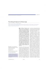
(a) THAB Model
A A B B F(A,A,B,B) G(A,A,B,B)
4
1
(b) Architecture
EVM
np < n
INA
Computing Element
I-V Curve
5 SO
CFM
RI
2
3 (c) State Machine
Fig. 1: Snider’s Boolean Logic Circuits
II. BACKGROUND AND R ELATED W ORK This section describes the memristor model, data representation, control voltages, and the working principle of the previously proposed Boolean logic circuits [24]. A. Memristor Model Although memristors have different physical mechanisms [12,13,27], their circuit-level behaviour can be abstracted by two parameters: switching threshold voltage Vth (with or without a minimum voltage requirement for resistive switching) [28] and resistive switching behaviour (abrupt or smooth) [29]. Note that these two parameters are independent of each other. In this paper, we use a simplified memristor model based on a switching threshold voltage and abrupt switching [23,24]. For simplicity, this type of model is referred to as THAB (THreshold-ABrupt) memristor model. The top part of Fig. 1(a) illustrates the current-voltage relation of THAB model. The memristor switches from one resistive state to another when the absolute value of the voltage (either positive or negative) across the device is greater than its threshold voltage Vth ; see I-V curve of Fig. 1(a). Otherwise, it stays in its current resistive state. Normally, a memristor requires two different switching threshold voltages to switch from low to high resistance (RESET) and from high to low resistance (SET) [28,30]; see the bottom part of Fig. 1(a). The black squares represent the positive terminal of the memristor. For simplicity, we assume that THAB model has the same threshold voltage Vth (in absolute value) for both of them. B. Data Representation and Control Voltages A memristor has two resistive states: a high (Rof f ) and low (Ron ) resistance. In this paper, all logic circuits use Rof f and Ron for logic 1 and 0, respectively. It is worth to note that this is different from CMOS logic circuits which use high and low voltages to represent logic 1 and 0, respectively. To control memristor-based digital circuits, three different voltages are required: Vw , Vwh , and GND; see Fig. 1(a). Vw is used to program the resistance of a memristor; Vwh is used to minimize the impact of sneak path currents by halfselect voltage strategy [17]; Vwh is then applied to memristors
which are not involved in particular operations. Vwh is also used to support the implementation of basic logic gate as in the case of NAND [24]. The relationship between Vw , Vwh , GND and Vth is 0