This spatial multiplexing lets reduce the size and therefore the cost of the ... reconfiguration can then take advantage of this evolvable feature to design specific ...
PRIME 2007 10.3
Flexible Hardware for Fingerprint Image Processing Francisco Fons, Mariano Fons, Enrique Cantó
Mariano López
Dep. d’Enginyeria Electrònica, Elèctrica i Automàtica Universitat Rovira i Virgili Tarragona, Spain
Departament d’Enginyeria Electrònica Universitat Politècnica de Catalunya Vilanova i la Geltrú, Spain
Abstract—Reconfigurable computing adds to the traditional hardware/software design flow a new degree of freedom in the development of electronic systems. In a system-on-chip platform, the fact that a MCU makes evolve at run-time a hardware coprocessor mapped on a FPGA, to execute thus different compute-intensive tasks in the same silicon-area, results in a clear earned value applied to the system implementation: the low-cost reached through the resources time-multiplexing. Under that approach, this work merges both reconfigurable computing and HW/SW co-design technologies to develop an efficient architecture of an automatic fingerprint authentication system (AFAS) oriented to real-time embedded applications.
additional reconfiguration latency needed to swap the HW contexts, i.e. when a specific processor has finished its execution, it can be overwritten with another bitstream to place there a new controller responsible for the next task [2]. Although a clear tradeoff between silicon-area and execution time arises in this approach, all those specific applications that tolerates the time overhead due to the resources reconfiguration can then take advantage of this evolvable feature to design specific HW/SW applications, providing thus the efficiency of custom HW coprocessors as well as the flexibility and low-cost given by the run-time reconfiguration and silicon-saving features. This work focuses on exploiting all these challenging concepts in the HW/SW co-design of an automatic fingerprint authentication system (AFAS). Section II briefly presents the computational demands of the biometric recognition algorithm. Section III concentrates on the HW/SW architecture of the fingerprint computer and the reconfiguration strategy of the different HW coprocessors that take part in the system. The most relevant experimental results of this work-in-progress are shown in section IV. Finally, section V highlights some conclusions and points out about the future work.
I.
INTRODUCTION
Nowadays, innovative products like smart cards or personal data assistants (PDA) make continuous demands on embedded systems: high performance, high flexibility, low power consumption and mainly low-cost become more and more key features for all this kind of applications. Thus, there exist clear trends towards replacing the typical system architecture based on a SW-focused microcontroller unit (MCU) by a HW/SW system-on-chip (SoC) which not only integrates a processor core, standard peripherals and embedded memory as the MCU does but also programmable logic resources. As prices for field programmable gate arrays (FPGA) come down, these devices are reaching broader acceptance in the market. That is particularly true in those compute-intensive fields where high speed signal processing is required, as image processing applications [1]. Reconfigurable computing contributes to open the doors to the HW/SW co-design technology by emphasizing the need of flexible hardware solutions that can be ported to realworld applications. The role of evolvable hardware, in comparison with a static implementation of a conceptually identical hardware processor, focuses on partitioning that application in a chain of tasks sequentially executed under the same substrate of programmable resources. The whole functionality gets thus distributed in several hardware contexts processed one by one whereas the system behavior results the same as the one performed by the static design. This spatial multiplexing lets reduce the size and therefore the cost of the programmable device in exchange for adding
This work has been supported by Ministerio de Educación y Ciencia, SPAIN, under grant TEC2006-12365-C02-02.
1-4244-1001-0/07/$25.00 ©2007 IEEE.
II. FINGERPRINT IMAGE PROCESSING Fingerprint matching is one of the most popular and reliable biometric techniques used in automatic personal identification. In fact, both industrial and scientist communities have recently addressed its attention and efforts on it: a lot of research groups are nowadays focused on developing accurate computing systems capable of recognizing the identity of a person at real-time and with good levels of trust. Although the biometric recognition algorithms and the fingerprint sensors have experienced big advances in the last years, the physical implementation of an AFAS is, still today, an open issue: in general, a state-of-theart recognition system works properly with good-quality images under powerful PC platforms but, nevertheless, its accuracy and performance drastically drops when either the quality characteristics of that image decreases or the computing algorithm is ported to embedded MCU-based platforms, fact that advice us to take care about applying these systems in those real-world scenarios where features as safety and ergonomics have a high impact.
PRIME 2007 10.3
As procedure, the user sweeps his finger through the fingerprint sensor surface and a digital fingerprint image is captured giving rise to an 8-bit gray-scale bitmap of typically 500 dpi resolution. From that moment on, the acquired image is submitted to a sequence of computationally extensive stages that finally let send out a verdict about whether that user fingerprint sample matches the enrolled fingerprint template to authenticate thus its owner: image segmentation, normalization, binarization, thinning, features extraction and matching are the typical computing stages followed by the AFAS algorithm. In general, in whatever image processing technique that process a pixel-based input image to generate an output image, each pixel of the output image gets dependant not only on the value of the input pixel located there but also on its neighbors, where the neighborhood depth is given by the kernel size of the applied filter. Just for this reason, the 2-D convolution is one of the fundamental primitives in any digital image processing technique. Its compute-intensive nature, based on an arithmetic sum of products, is the key factor for reaching an efficient implementation of those processors dedicated to enhance or extract important information contained in the image [3]. Mathematically it is expressed as:
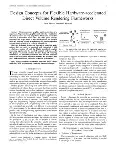
embedded processor stripe, i.e. MCU, constituted by an ARM922T core processor, standard peripherals such as UART and timers, and both on-chip SRAM and DPSRAM memory blocks. In connection with the embedded processor, up to 1Mbit of logical gates are present in the APEX20KE FPGA, ready to place there custom-made HW coprocessors. Both MCU and FPGA are merged in a single-chip and connected under two AMBA AHB bus interfaces, as well as DPSRAM via an AVALON interface, to share data between MCU and FPGA, and a specific configuration controller from where the MCU can reconfigure the FPGA while the system continues active. Other resources located in the development board are also: FLASH memory, to store the different configuration data, not only the MCU program code but also the different bitstreams corresponding to the HW contexts that are dynamically downloaded into the FPGA while the application is in progress, and SDRAM memory, to store the whole acquired fingerprint image and the next resultant images processed along the following stages of the algorithm, as depicted in Fig. 1. AUTOMATIC FINGERPRINT AUTHENTICATION SYSTEM SDRAM (finger images)
K y Kx
p' ( y, x ) = ∑∑p( y + j, x + i )h( j, i ) j
(1)
i
where p’(y,x) is the output pixel, p(y,x) is the pixel of the input image and h is the convolution filter with kernel Ky·Kx. This computation is also the basic operation used in most of the digital processing stages of the fingerprint recognition algorithm, where the constant coefficients h of the convolution are customized in accordance with the specific stage to process (Sobel operators for the gradient computing, Dyadic Scale-Space or Gabor filters in the image enhancement, etc). III.
SYSTEM ARCHITECTURE
This work goes in search of an efficient architecture suitable for embedded automatic fingerprint recognition systems. For this, a SW-only implementation of the biometric algorithm is compared with a HW/SW solution based on reconfigurable HW, in order to highlight the pros and cons of each option in terms of performance and cost. In the first approach, all the computing is carried out by a MCU. In the second one, this same computational load is partitioned into HW and SW tasks where a FPGA takes charge of the computation while a MCU controls the program flow by reconfiguring, at run-time, the HW coprocessors fitted in the FPGA at each stage of the biometric algorithm. The architecture is particularly oriented to embedded applications, as consumer electronic products, e.g. a PDA with an integrated fingerprint sensor that deploys the function of authenticating the user. The HW/SW platform used in this work is constituted by an Altera EPXA10 SoC [4] and an Atmel FCD4B14 fingerprint sensor [5]. The Excalibur EPXA10 SoC device combines an
EXCALIBUR EPXA10 SYSTEM-ON-CHIP ARM922T CORE AMBA AHB1 SDRAM CONTROLLER
AHB BRIDGE
SRAM (program code)
DPSRAM (data)
AMBA AHB2 FLASH (bitstreams)
CONFIGURATION CONTROLLER
EBI
EXTERNAL LINK (debug purposes)
UART
FINGERPRINT SENSOR
APEX20K FPGA
AHB BRIDGE
AHB BRIDGE
AHB SLAVE
AHB MASTER
AVALON CONTROLLER
COMPUTER PARAMETERS
RECONFIGURABLE COMPUTING Context A: SGMNT & NORM. Context B: DSS FILTER Context C: FIELD ORIENT.
LPM DPRAM
FSM CONTROLLER
SPECIFIC ALU
Figure 1. System architecture.
The stage corresponding to the fingerprint image acquisition and reconstruction, although it has also been developed, is not covered in this paper. In that phase, the image is captured by the thermal sweeping sensor giving rise to a set of image slices. Next, the total image is reconstructed by connecting each pair of consecutive slices through the common overlapped lines of pixels between them. This process, carried out by the MCU, results in a whole fingerprint image of 512x256 effective pixels located into SDRAM from where both MCU and FPGA can access to it [6]. The following stages refer to the first stages of the fingerprint image enhancement algorithm: segmentation, normalization, noise suppression and field orientation. All these stages, already evaluated in this work, carry out a 2-D convolution of the fingerprint image as the most demanding computational task involved in the image processing. These stages are described next in this section: A. Image Segmentation and Normalization The acquired fingerprint image is generally split in two regions: the foreground or region of interest, characterized by the skin ridges and valleys of sequential clear and dark tones, and the background or region with no information,
PRIME 2007 10.3
which normally shows a continuous tone. These differences of tonality present in the gray-scale image let implement the segmentation algorithm based on the gradient computation. The gradient operator applied in this work is the Sobel convolution mask. Concerning size, a kernel 5x5 is considered to calculate the gradient at each pixel of the input image. Then, the whole fingerprint image is divided in blocks of 8x8 pixels and the segmentation criterion is applied to each one of these unitary blocks: a block is removed or, on the contrary, it remains in the image depending on its resultant gradient value compared with a segmentation threshold. For this, the algorithm computes the directional gradient terms gY and gX at each pixel and accumulates the absolute value of both components for the 8x8 pixels of each block to finally approximate the gradient magnitude as: 8
8
8
8
j
i
j
i
G8 x8 ( y, x ) = ∑∑gY ( y + j, x + i ) + ∑∑g X ( y + j, x + i ) . (2)
After the segmentation, the image normalization pursues to reduce the gray-level variations among ridges and valleys. In this way, the input image is pixel-by-pixel normalized until achieving a processed fingerprint image with a pre-specified mean and variance [7]. B. Image Noise Suppression A typical processing stage carried out in an automatic fingerprint authentication system is to recover the image information from those areas that have been corrupted by the noise in the fingerprint acquisition phase. For this, as part of our enhancement algorithm, we make use of the Dyadic Scale-Space (DSS) theory. This strategy lets restore the ridges and valleys of those low quality regions of the fingerprint image by decomposing it into a series of images to remove the noise in different scales. Finally, all these processed images are combined again to reach a more credible fingerprint image [8]. As result, the normalized image is convolved with a gaussian filter to obtain a enhanced image that preserves the valid information previously lost due to the noise. In our implementation, the DSS convolution mask is a symmetric kernel 13x13. C. Image Field Orientation The least mean square orientation algorithm is used to estimate the orientation field of the fingerprint image [7]. The enhanced image coming from the DSS algorithm is now divided in 8x8 sectors and the gradient is computed again for each pixel. The local orientation of each block 8x8 is now computed using the equation: ⎞ ⎛ 8 8 ⎜ ∑∑2 g X ( y + j, x + i ) gY ( y + j, x + i ) ⎟ 1 ⎟ (3) ⎜ θ 8 x 8 ( y, x ) = tan −1 ⎜ 8 j 8 i ⎟. 2 ⎜ ∑∑(g X2 ( y + j, x + i ) − g Y2 ( y + j , x + i ) ) ⎟ ⎟ ⎜ ⎠ ⎝ j i
From a HW point of view, some optimizations have been done in the algorithm: all the divisions have been converted into products and shifts, floating-point operands are skipped and substituted by fixed-point operations, and some mathematical expressions have been rewritten in order to optimize its processing. Thus, for instance, the expression gX2-gY2 can be reworked as (gX+gY)·(gX-gY), since the synthesis of a multiplier takes much more area than an adder. Moreover, the HW-SW performance of real-time image processing applications mainly depends on the data bandwidth handled. Like this, our platform makes use of a 32-bit AMBA AHB interface to link MCU, FPGA and SDRAM. The MCU is the AFAS master processor and it dictates the application flow. Some of the tasks are directly executed by the MCU and others are carried out in parallel by the FPGA. The HW tasks covered in this paper are divided in three different contexts: in a first context a HW coprocessor takes charge of computing both image segmentation and normalization, a second context performs the image DSS-based filtering and a third context fits a coprocessor that computes the field orientation of the resultant image. Although each context implements a dedicated HW coprocessor made to measure of the specific computing task, all these FPGA-based coprocessors hold a similar architecture of functional blocks with a defined role, as shown in Fig. 1: •
The AHB master controller takes charge of transferring the fingerprint image from the SDRAM to the internal LPM DPRAM in format of Y-slices to be processed. In the same way, the resultant image computed in each phase is sent back to SDRAM where the total image keeps stored.
•
The internal LPM DPRAM dual-port memory becomes a data buffer or cache that feeds the 2D-convolver with the kernel of pixels required in each phase.
•
Through an AHB slave controller, the MCU, before launching a HW task, configures the HW coprocessor by writing to some specific FPGA registers used as flexible parameters, such as the Y and X dimensions of the image or other customizable settings as the segmentation threshold value, etc.
•
The core of the HW coprocessor is the specific ALU. This is basically the only part that differs from one stage to the next one, depending on the particular arithmetic computing required each time, e.g. a MAC (multiplyaccumulate) unit or a trigonometric CORDIC unit, handled by its particular finite state machine (FSM). IV.
PERFORMANCE EVALUATION
In a first approach, the image segmentation, normalization, noise suppression and field orientation computing processes are carried out only by SW tasks executed on the MCU running at 50 MHz. The results concerning time performance are really poor. Next, these same four phases are synthesized on hardware through three independent reconfigurable coprocessors that the MCU
PRIME 2007 10.3
sequentially downloads in the FPGA at run-time, following the sequential execution of the biometric recognition algorithm. In this second scenario, the FPGA takes charge of the computing tasks while the MCU is responsible for handling the application flow by reconfiguring the HW coprocessors placed in the FPGA at each phase [4]. In this approach, both MCU and FPGA work at 50 MHz. The performances comparison is collected in Table I. The results show that the throughput of the image processing algorithm notoriously improves when it is executed under specific hardware instead of under a general-purpose microprocessor. TABLE I.
EXECUTION TIME
Timing Performances (ms)
Sequential Contexts
SW (MCU)
Fingerprint Image Processing
Context A
Segmentation & Normalization
Context B
Dyadic Scale-Space Filtering
Context C
Field Orientation
HW-SW (FPGA)
1575
25
18500
35
1970
25
In the HW-SW approach, in addition to the HW processing time, the time spent by the MCU to fully reconfigure the 1 Mgates FPGA and switch from one context to the next one is 720 ms. This process is carried out through the configuration controller at 16 MHz. Some details regarding to the architecture of the image convolver are gathered in Fig. 2. The convolver dimensions are adjusted in each context to the filter size required each time. Other coprocessors are also present to complement every digital processing stage, as detailed in the table illustrated in Fig. 2. 512 …
LPM LPM DPRAM DPRAM 512x32 512x32
X 280
280
The resources involved in each context are summarized in Table II. Our solution would fit in a reconfigurable FPGA of about 12k logic cells, 5k registers and 64 kbits of memory, amount of resources that, on the other hand, would notoriously increase if the same design was statically performed providing all the HW contexts at the same time. TABLE II.
HARDWARE RESOURCES Hardware Performances
Sequential Contexts
Image Processing
Context A
Segm. & Norm.
1384
4729
38912
Context B
DSS Filtering
5022
11639
65536
Context C
Field Orient.
1513
9123
36864
V.
One-bit Registers
Logic Cells
Memory Bits
CONCLUSIONS AND FUTURE WORK
This work presents an innovative system architecture applied to an embedded automatic fingerprint recognition system. A SW-only solution has been compared with a HW/SW approach based on reconfigurable hardware. The results prove that a set of reconfigurable HW coprocessors mapped on a middle-range FPGA lets customize each stage of the biometric algorithm and reduce the execution time –in spite of the overhead given by the HW context reconfiguration– in about two orders of magnitude, fact that converts the HW/SW approach in a valid solution for realtime applications where the SW-only option would not be feasible due to its low performance. Until now, this architecture has been tested on the first stages of the biometric recognition algorithm. As future work, the authors pursue to develop the remaining stages of the algorithm to reach thus a complete embedded AFAS solution.
…
REFERENCES
Y-shift 3 2 1
[1]
1 2 3 ... 516 Y (1,1)
516
MUX 2x32 MUX 2x32 509 510 511 512 … 5 1
6 2
7 3
513 514 515 516 …
8 4
9 5
10 6
280 … 3 2 1
5 SHIFT REGISTERS 8-BYTE
11 7
X-shift
12 8
HARDWARE RESOURCE
CONTEXT A
CONTEXT B
CONTEXT C
image lpm dpram
2 blocks 512x32
4 blocks 512x32
2 blocks 512x32
multiplexors
2 mux 2x32
4 mux 4x32
2 mux 2x32
shift registers
5x8 8-bit data
13x16 8-bit data
5x8 8-bit data
pixels’ kernel
5x5
13x13
5x5
convolution technique
add-shift unit
vector multiplier
add-shift unit
lpm ramdp data acc.
3 blocks 64x32
0 blocks
2 blocks 64x32
abs(a) (gradient)
y=a+bx (normalization)
convolver (gradient)
convolver (gradient)
neg-saturation (normalization)
∑ a·b (field orient.)
∑a (mean)
pos-saturation (normalization)
∑ ((a+b)·(a-b)) (field orient.)
∑ a·a (variance)
convolver (DSS)
tan-1 (b/a) (CORDIC)
segmented image
normalized & filtered image
image field orientation
4 KERNEL 5x5 8-BIT main arithmetic coprocessors synthesized
∑∑pji·hji ∑∑pji·hji 8 CONVOLVERS
∑∑pji·hji ∑∑pji·hji
gX[0] gX[1] gX[2] gY[0] gY[1] gY[2]
gX[3] gY[3]
partial result
Figure 2. HW coprocessors features.
[2]
[3] [4] [5] [6]
[7]
[8]
C-J. Chang, P-Y Hsiao and Z-Y Huang, “Integrated operation of image capturing and processing in FPGA,” IJCSNS International Journal of Computer Science and Network Security, vol. 6, no. 1A, pp. 173-180, January 2006. E. Cantó, J.M. Moreno, J. Cabestany, I. Lacadena and J.M. Inserser, “A temporal bipartitioning algorithm for dynamically reconfigurable FPGAs,” IEEE Transactions on Very Large Scale Integration (VLSI) Systems, vol. 9, no. 1, pp. 210-218, February 2001. Atmel Corp., “3x3 convolver with run-time reconfigurable vector multiplier in Atmel AT6000 FPGAs,” www.atmel.com. Altera Corp., “Reconfiguring Excalibur devices under processor control,” www.altera.com. Atmel Corp., “FCD4B14 FingerChip”, www.atmel.com M. Fons, F. Fons, N. Canyellas, E. Cantó and M. López, “Hardwaresoftware co-design of an automatic fingerprint acquisition system”, Proc. IEEE International Symposium on Industrial Electronics, vol. 3, pp. 1123-1128, June 2005. L. Hong, Y. Wan and A. Jain, “Fingerprint image enhancement: algorithm and performance evaluation,” IEEE Transactions on Pattern Analysis and Machine Intelligence, vol. 20, no. 8, pp. 777-789, 1998. J. Cheng and J. Tian, “Fingerprint enhancement with dyadic scalespace,” Pattern Recognition Letters 25, Ed Elsevier, pp. 1273-1284, 2004.