CERTIFICATE. This is to certify that the thesis entitled “FPGA implementation of
artificial neural networks” submitted by Sri Pankaj Sharma in partial fulfillment of ...
FPGA IMPLEMENTATION OF ARTIFICIAL NEURAL NETWORKS
A THESIS SUBMITTED IN PARTIAL FULFILLMENT OF THE REQUIREMENTS FOR THE DEGREE OF
BACHELOR OF TECHNOLOGY IN ELECTRICAL ENGINEERING.
By Bhaskar Bateja Roll No. – 10302061 And Pankaj Sharma Roll No. – 10302011
Department of Electrical Engineering National Institute of Technology, Rourkela
FPGA IMPLEMENTATION OF ARTIFICIAL NEURAL NETWORKS
A THESIS SUBMITTED IN PARTIAL FULFILLMENT OF THE REQUIREMENTS FOR THE DEGREE OF
BACHELOR OF TECHNOLOGY IN ELECTRICAL ENGINEERING. By
Pankaj Sharma Roll No. – 10302011
Under the guidance of Dr. Pradipta Kumar Nanda
Department of Electrical Engineering National Institute of Technology, Rourkela
National Institute of Technology Rourkela
CERTIFICATE This is to certify that the thesis entitled “FPGA implementation of artificial neural networks” submitted by Sri Pankaj Sharma in partial fulfillment of the requirements for the award of Bachelor of Technoloy Degree in Electrical Engineering at National Institute of Technology, Rourkela (Deemed University) is an authentic work carried out by him under my supervision and guidance.
To the best of my knowledge, the matter embodied in the thesis has not been any other University/ Institute for the award of any degree or diploma.
Dr. P. K. Nanda Date:
Professor and Head, Department of Electrical Engg. National Institute of Technology Rourkela - 769008
i
ACKNOWLEDGEMENT No thesis is created entirely by an individual, many people have helped to create this thesis and each of their contribution has been valuable. My deepest gratitude goes to my thesis supervisor, Dr.P.K.Nanda, Professor, Department of Electrical Engineering, for his guidance, support, motivation and encouragement through out the period this work was carried out. His readiness for consultation at all times, his educative comments, his concern and assistance even with practical things have been invaluable. I would also like to thank all professors and lecturers, and members of the department of Electrical Engineering for their generous help in various ways for the completion of this thesis. A vote of thanks to my fellow students for their friendly co-operation.
Pankaj Sharma Roll. No. 10302011 Dept. Of Electrical Engineering NIT Rourkela
ii
TABLE OF CONTENTS 1. List of Figures
iv
2. Introduction
1
3. Survey of hardware implementations of Artificial Neural Networks
3
3.1 Comparison between analog and digital implementations of ANN’s
4
2.2 Hardware implementations using FPGAs 3. FPGA implementation issues
4 6
3.1 A brief introduction to FPGA’s
7
3.2 Implementation issues
8
3.2.1 Learning algorithm
9
3.2.2 Signal presentation
9
3.2.3 Multiplier reduction schemes
11
4. Implementation Approaches
12
4.1 A brief introduction to ANN
13
4.2 Implementation Approaches
17
4.2.1 Non RTR approach
17
4.2.2 RTR approach
18
5. Implementation of multilayer ANN for XOR problem
20
5.1 Introduction to XOR problem
21
5.2 Implementation Approach
22
5.3 VHDL program
23
6. References
31
iii
LIST OF FIGURES Figure 3.1: - General architecture of Xilinx FPGAs. Figure 3.2: - Virtex-E Configurable Logic Block Figure 3.3: - Signal Representation Figure 4.1: - The perceptron model Figure 4.2: - Multilayer perceptron Figure 4.3: - The sigmoid function Figure 4.4: - RTR and NON – RTR Approach Figure 5.1: - The XOR Problem Figure 5.2: - 5 neuron model for XOR Problem.
iv
Chapter 1
INTRODUCTION
1
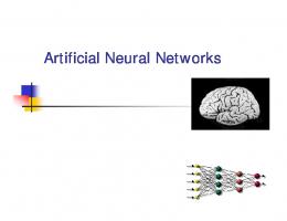
As the title suggests our project deals with a hardware implementation of artificial neural networks, specifically a FPGA implementation. During the course of this project we learnt about ANNs and the uses of such soft computing approaches, FPGAs, VHDL and use of various tools like Xilinx ISE Project Navigator and ModelSim. As numerous hardware implementations of ANNs already exist our aim was to come up with an approach that would facilitate topology evolution of the ANN as well. The key problem in the simulation of ANN’s is its computational overhead. Networks containing millions of neurons and ten billion connections, and complex models like spiking neurons with temporal time course that require convolutions to be computed at each synapse, will challenge even the fastest computers. Hence there is much interest in developing custom hardware for ANN’s. Points in favor of hardware implementations are: a) Inherent parallelism and connectionist model of ANN’s which find a natural application through hardware. General purpose processors operate sequentially. b) Simple ANN models require simple, low precision computations which can be performed faster on cheap and low precision hardware. Also since hardware is getting cheaper by the day, custom hardware can be built to perform complex computations. Field Programmable Gate Arrays (FPGA) are a type of hardware logic device that have the exibility to be programmed like a general-purpose computing platform (e.g. CPU), yet retain execution speeds closer to that of dedicated hardware (e.g. ASICs). Traditionally, FPGAs have been used to prototype Application Specific Integrated Circuits (ASICs) with the intent of being replaced in _nal production by their corresponding ASIC designs. Only in the last decade have lower FPGA prices and higher logic capacities led to their application beyond the prototyping stage, in an approach known as reconfigurable computing. A question remains concerning the degree to which reconfigurable computing has benefited from recent improvements in the state of FPGA technologies / tools. This thesis presents a Reconfigurable Architecture for Implementing ANNs on FPGAs as a case study used to answer this question.
2
Chapter 2
A SURVEY OF HARDWARE IMPLEMENTATIONS OF ARTIFICIAL NEURAL NETWORKS Comparison between analog and digital implementations of ANNs Hardware implementations using FPGAs
3
2.1 Comparison between analog and digital implementations of ANN’s Intuitively analog seems a better choice as it would be better to represent synaptic weights by analog quantities. Computational density of analog chips is greater. Complex, non-linear functions like multiply, divide and hyperbolic tangent can be performed with a handful of transistors. Power required for these computations is less than with digital methods. However, people are more familiar with digital design now i.e. analog design is an uncommon capability. Most applications comprise of digital systems and a digital neural network will provide ease in integration with these systems. Analog designs are hardwired and thus inflexible. Digital designs are flexible as in they employ part software control, arbitrary precision and reprogammability. This enables them to solve a larger part of the problem at the price of reduced performance/cost. Signal interconnection is also a problem. Wire interconnections in silicon are expensive and take up more area. The solution has to be multiplexing of connections i.e. multiple synaptic connections share the same wire. This adds to the complexity if the design but results in a massive reduction in cost. Analog designs are hard to multiplex. Amadahl’s law states that no matter how many processors are available to execute a subtask, the speed of a particular task is roughly proportional to the number of subtasks that have to be executed sequentially. Thus a programmable device that accelerates several phases of an application offers more benefits than a dedicated device.
2.2 Hardware implementations using FPGAs This is the most promising method. The structure of FPGA’s is suitable for implementations of ANN’s. FPGA-based reconfigurable computing architectures are well suited for implementations of neural networks as one may exploit concurrency and rapidly reconfigure for weight and topology adaptation. All FPGA implementations attempt to exploit the reconfigurability if FPGA’s.
4
Identifying the purpose of reconfiguration sheds light on the different implementation approaches. 1. Prototyping and simulation: FPGA’s can be reconfigured an innumerable number of times. This allows rapid prototyping and direct simulation in hardware, which also increases the speed of the simulation and can be used to test various ANN implementations and learning algorithms. 2.
Density enhancement: This is the increase in the functional capacity per unit area of the chip. Density enhancement can be done in two ways. A) It is possible to time multiplex an FPGA chip for each of the sequential steps in an ANN algorithm. Each stage occupies the same entire hardware resource and the resource is configured for the stage which is reached. B) Dynamic constant folding: In this case the FPGA chip is time multiplexed for each of the ANN circuits that is specialized with a step of constant operands in different stages during execution. Both these methods incur a reconfiguration time overhead and are suitable only until a
certain break even point below which the computation time is much smaller than reconfiguration time. 3. Topology adaptation: Dynamically reconfigurable FPGA’s permit ANN algorithm with topology adaptation along with weight adaptation. The role which a FPGA-based platform plays in neural network implementation, and what part(s) of the algorithm it's responsible for carrying out, can be classified into two styles of architecture, as either a co-processor or as a stand-alone architecture. When taking on the role of a co-processor, a FPGA-based platform is dedicated to offoading computationally intensive tasks from a host computer. In other words, the main program is executed on a general-purpose computing platform, and certain tasks are assigned to the FPGA-based coprocessor to accelerate their execution. For neural networks algorithms in particular, an FPGA-based co-processor has been traditionally used to accelerate the processing elements (eg. neurons. On the other hand, when a FPGA-based platform takes on the role of a stand-alone architecture, it becomes self-contained and does not depend on any other devices to function. In relation to a co-processor, a stand-alone architecture does not depend on a host computer, and is responsible for carrying out all the tasks of a given algorithm. 5
Chapter 3
FPGA IMPLEMENTATION ISSUES
A brief introduction to FPGAs Implementation Issues
6
3.1 A brief introduction to FPGAs FPGAs are a form of programmable logic, which offer flexibility in design like software, but with performance speeds closer to Application Specific Integrated Circuits (ASICs). With the ability to be reconfigured an endless amount of times after it has already been manufactured, FPGAs have traditionally been used as a prototyping tool for hardware designers. However, as growing die capacities of FPGAs have increased over the years and so has their use in reconfigurable computing applications.
FPGA Architecture Physically, FPGAs consist of an array of uncommitted elements that can be interconnected in a general way, and is user-programmable. According to Brown et al. every FPGA must embody three fundamental components (or variations thereof) in order to achieve reconfigurability { namely logic blocks, interconnection resources, and I/O cells. Digital logic circuits designed by the user are implemented in the FPGA by partitioning the logic into individual logic blocks, which are routed accordingly via interconnection resources. Programmable switches found throughout the interconnection resources dictate how the various logic blocks and I/O cells are routed together. The I/O cells are simply a means of allowing signals to propagate in and out of the FPGA for interaction with external hardware. Logic blocks, interconnection resources and I/O cells are merely generic terms used to describe any FPGA, since the actual structure and architecture of these components vary from one FPGA vendor to the next. In particular, Xilinx has traditionally manufactured SRAM-based FPGAs; socalled because the programmable resources3 for this type of FPGA are controlled by static RAM cells. The fundamental architecture of Xilinx FPGAs is shown in Figure 3.1. It consists of a twodimensional array of programmable logic blocks, referred to as Configurable Logic Blocks (CLBs). The interconnection resources consist of horizontal and vertical routing channels found respectively between rows and columns of logic blocks. Xilinx's proprietary I/O cell architecture is simply referred to as an Input/Output Block (IOB). Note that CLB and routing architectures differ for each generation and family of Xilinx FPGA. For example, Figure 3.2 shows the architecture of a CLB from the Xilinx Virtex-E family of FPGAs, which contains four logic cells (LCs) and is organized in two similar slices. Each LC includes a 4-input look-up table (LUT), dedicated fast carry-lookahead logic for arithmetic functions, and a storage element (i.e. a flip-flop). A CLB from the Xilinx Virtex-II family of 7
FPGAs, on the other hand, contains over twice the amount of logic as a Virtex-E CLB. It turns out that the Virtex-II CLB contains four slices, each of which contain two 4-input LUTs, carry logic, arithmetic logic gates, wide function multiplexers, and two storage elements. As we will see, the discrepancies in CLB architecture from one family to another is an important factor to take into consideration when comparing the spatial requirements (in terms of CLBs) for circuit designs which have been implemented on different Xilinx FPGAs.
Figure 3.1: General Architecture of Xilinx FPGAs.
Figure 3.2: Virtex-E Configurable Logic Block
3.2 Implementation Issues FPGA implementations of neural networks can be classified on the basis of: 1. Learning Algorithm 2. Signal representation 3. Multiplier reduction schemes
8
3.2.1 Learning Algorithm The type of neural network used in FPGA-based implementations is an important feature used in classifying such architectures. The type of neural network applied depends on the intended application used to solve the problem at hand. A. Backpropagation Algorithm 1. RRANN Architecture by Elderedge 2. RENCO by Beuchat 3. ACME by Ferucci and Martin 4. ECX card by Skrbeck B. Ontogenic Neural Networks 1. FAST Architecture by Perez-Uribe. FAST was used to implement three different kinds of unsupervised, ontogenic neural networks, adaptive resonance theory (ART), adaptive heuristic critic (AHC), and Dyna-SARSA. C. Cellular Automata based neural networks 1. CAM- Brain Machine by de Garris. D. Modular Neural Networks 1. REMAP Architecture by Nordstrom.
3.2.2 Signal Representation Four common types of signal representations typically seen in ANN h/w architectures are: Frequency-based - is categorized as a time-dependent signal representation, since it counts the number of analog spikes (or digital 1's depending on h/w medium used) in a given time window (i.e. of n clock cycles). It is popularin analog hardware implementations. Spike Train - is categorized as a time- and space-dependent signal representation, since the information it contains is based on spacing between spikes (1's) and is delivered in the form of a real number (or integer) within each clock cycle. Used in the CBM. 9
Floating-point - is considered to be position-dependent because numerical values are represented as strings of digits. Floating-point as a signal representation for FPGA- based (i.e. digital) ANN architectures has been deemed as overkill. This is due to the fact that valuable circuit area is wasted in providing an over-abundance of range-precision, which is never fully utilized by most ANN applications.
Figure 3.3 Signal Representation
Fixed-point - is categorized as yet another position-dependent signal representation. Fixed-point is the most popular signal representation used among all the surveyed FPGA-based (i.e. digital) ANN architectures. This is due to the fact that fixed-point has traditionally been more areaefficient than floating-point, and is not as severely limited in range-precision as both, frequency and spike-train signal representations The issues related to fixed point signal representation are 1. Overflow and underflow 2. Convergence rates 3. Quality of generalization One way to help achieve the density advantage of reconfigurable computing over general purpose computing is to make the most efficient use of the hardware area available. In terms of an optimal range-precision vs area trade-off, this can be achieved by determining the minimum allowable precision and minimum allowable range, where their criterion is to minimize hardware area usage without sacrificing quality of performance. These two concepts combined can also be referred to as the minimum allowable range-precision. Holt and Baker showed that 16-bit fixedpoint was the minimum allowable range-precision for the backpropagation algorithm. However,
10
minimizing range precision (i.e. maximizing processing density) without affecting convergence rates is applications-specifc, and must be determined empirically. 3.2.3 Multiplier Reduction Schemes The multiplier has been identified as the most area-intensive arithmetic operator used in FPGAbased ANNs. Use of bit-serial multipliers - This kind of digital multiplier only calculates one bit at a time, whereas a fully parallel multiplier calculates all bits simultaneously. Hence, bit-serial can scale up to a signal representation of any range-precision, while its area-efficient hardware implementation remains static. However, the time vs. area trade-off of bit-serial means that multiplication time grows quadratically, with the length of signal representation used. Use of pipelining is one way to help compensate for such long multiplication times, and increase data throughput. Reduce range-precision of multiplier - achieved by reducing range-precision of signal representation used in (fully parallel-bit) multiplier. Unfortunately, this is not a feasible approach since limited range-precision has a negative effect on convergence rates, as discussed in previous section. Signal representations that eliminate the need for multipliers - Certain types of signal representations replace the need of multipliers with a less area-intensive logic operator. Perez-Uribe considered using a stochastic-based spike train signal his FAST neuron architecture, where multiplication of two independent signals could be carried out using a two-input logic gate. Nordstrom implemented a variant of REMAP for use with Sparse Distributed Memory (SDM) ANN types, which allowed each multiplier to be replaced by a counter preceded by an exclusive-or logic gate. Another approach would be to limit values to powers of two, thereby reducing multiplications to simple shifts that can be achieved in hardware using barrel shifters. Unfortunately, this type of multiplier reduction scheme is yet another example where use of limited range-precision is promoted. Such a scheme would jeopardize ANN performance (i.e. convergence rates) and should be avoided at all costs.
11
Chapter 4
IMPLEMENTATION APPROACHES
A brief introduction to ANN Implementation Approaches
12
4.1 A brief introduction to ANN Artificial neural networks (ANNs) are a form of artificial intelligence, which have been modelled after, and inspired by the processes of the human brain. Structurally, ANNs consist of massively parallel, highly interconnected processing elements. In theory, each processing element, or neuron, is far too simplistic to learn anything meaningful on its own. Significant learning capacity, and hence, processing power only comes from the culmination of many neurons inside a neural network. The learning potential of ANNs has been demonstrated in different areas of application, such as pattern recognition, function approximation/prediction, and robot control
Figure 4.1 The Perceptron Model
Backpropagation Algorithm ANNs can be classified into two general types according to how they learn – supervised or unsupervised. The backpropagation algorithm is considered to be a supervised learning algorithm, which requires a trainer to provide not only the inputs, but also the expected outputs. Unfortunately, this places added responsibility on the trainer to determine the correct input/output patterns of a given problem a priori. Unsupervised ANNs do not require the trainer to supply the expected outputs.
Figure 4.2 Multilayer Perceptron
13
According to Rumelhart et al. an ANN using the backpropagation algorithm has five steps of execution: Initialization- The following initial parameters have to determined by the ANN trainer a priori: •
w(s)kj (n) is defined as the synaptic weight that corresponds to the connection from neuron unit j in the (s - 1)th layer, to k in the sth layer of the neural network. This weight was calculated during the nth iteration of the backpropagation, where n = 0 for initialization.
•
η is defined as the learning rate and is a constant scaling factor used to control the step size in error correction during each iteration of the backpropagation algorithm. Typical values of η range from 0.1 to 0.5.
•
θ(s)k is defined as the bias of a neuron, which is similar to synaptic weight in that it corresponds to a connection to neuron unit k in the sth layer of the ANN, but is NOT connected to any neuron unit j in the (s - 1)th layer. Statistically, biases can be thought of as noise, which better randomizes initial conditions, and increases the chances of convergence for an ANN. Typical values of θ(s)k are the same as those used for synaptic weights w(s)kj (n) in a given application.
Presentation of Training Examples- Using the training data available, present the ANN with one or more epoch. An epoch, as defined by Haykin, is one complete presentation of the entire training set during the learning process. For each training example in the set, perform forward followed by backward computations consecutively. Forward Computation- During the forward computation, data from neurons of a lower layer (i.e. (s-1)th layer), are propagated forward to neurons in the upper layer (i.e. sth layer) via a feedforward connection network. The structure of such a neural network is shown in Figure 4.1, where layers are numbered 0 to M, and neurons are numbered 1 to N. The computation performed by each neuron during forward computation is as follows: Equation 4.1
, where j < k and s = 1; : : : ;M 14
H(s)k = weighted sum of the kth neuron in the sth layer w(s)kj = synaptic weight which corresponds to the connection from neuron unit j in the (s - 1)th layer to neuron unit k in the sth layer of the neural network o(s-1)j = neuron output of the jth neuron in the (s - 1)th layer θ(s)k = bias of the kth neuron in the sth layer Equation 4.2, where k = 1; : : : ;N and s = 1; : : : ;M o(s)k = neuron output of the kth neuron in the sth layer f(H(s)k ) = activation function computed on the weighted sum H(s)k Note that some sort of sigmoid function is often used as the nonlinear activation function, such as the logsig function shown in the following: Equation 4.3
Figure 4.3 The Sigmoid Function
Backward Computation- The backpropagation algorithm is executed in the backward computation, although a number of other ANN training algorithms can just as easily be substituted here. Criterion for the learning algorithm is to minimize the error between the expected (or teacher) value and the actual output value that was determined in the Forward Computation. The backpropagation algorithm is defined as follows: 1. Starting with the output layer, and moving back towards the input layer, calculate the local gradients, as shown in Equations 4.4., 4.5, and 4.6. For example, once all the local 15
gradients are calculated in the sth layer, use those new gradients in calculating the local gradients in the (s -1)th layer of the ANN. The calculation of local gradients helps determine which connections in the entire network were at fault for the error generated in the previous Forward Computation, an is known as error credit assignment. 2. Calculate the weight (and bias) changes for all the weights using Equation 4.7. 3. Update all the weights (and biases) via Equation 4.8. Equation 4.4
, where ε(s)k = error term for the kth neuron in the sth layer; the difference between the teaching signal tk and the neuron output o(s)k δ(s+1)j = local gradient for the jth neuron in the (s + 1)th layer. Equation 4.5
, where f’(H(s)k) is the derivative of the activation function , which is actually a partial derivative of activation function w.r.t net input (i.e. weight sum), or
Equation 4.6 , where a(s)k = f(H(s)k ) = osk
Equation 4.7 , where Δw(s)kj is the change in synaptic weight (or bias) corresponding to the gradient of error for connection from neuron unit j in the (s - 1)th layer, to neuron k in the sth layer. Equation 4.8 , where k = 1; : : : ;Ns and j = 1; : : : ;Ns-1 wskj (n + 1) = updated synaptic weight (or bias) to be used in the (n + 1)th iteration 16
of the Forward Computation Δw(s)kj (n) = change in synaptic weight (or bias) calculated in the nth iteration of the Backward Computation, where n = the current iteration w(s)kj (n) = synaptic weight (or bias) to be used in the nth iteration of the Forward and Backward Computations, where n = the current iteration.
Iteration- Reiterate the Forward and Backward Computations for each training example in the epoch. The trainer can continue to train the ANN using one or more epoch until some stopping criteria (eg. low error) is met. Once training is complete, the ANN only needs to carry out the Forward Computation when used in application.
4.2 Implementation Approaches Basically when implementing the backpropagation algorithms on FPGAs there are two approaches 1. Non-RTR Approach 2. RTR Approach RTR stands for Run-Time-Reconfiguration.
4.2.1 Non-RTR Approach The salient features of this approach are: All the stages of algorithm reside inside the FPGA at once. For the backpropagation algorithm the hardware elements required are adders, subtracters, multipliers and transfer function implementers. A finite state machine oversees the sequential execution of the stages using the afore mentioned hardware elements. The key design factor is the efficient use of the limited FPGA resources i.e. efficient design of the hardware components.
17
Performance enhancement can be achieved through: 1. Proper selection of parameters like range-precision. 2. Efficient design of the hardware components used. 3. Pipelining 1. Floating point representations have highest range-precision but require the largest area on chip. Fixed point is more area efficient and can provide acceptable range-precision. Holt and Baker showed that 16-bit fixed-point was the minimum allowable range-precision for the backpropagation algorithm. However, minimizing range precision (i.e. maximizing processing density) without affecting convergence rates is application-specific, and must be determined empirically. One challenge in implementing the backpropagation on FPGAs is the sequential nature of processing between layers. A major challenge is that pipelining of the algorithm on a whole cannot occur during training due to the weight update dependencies of backpropagation, and as a result, the utilization of hardware resources dedicated to each of the neural network's layers is wasted. However, it's still possible to use fine-grain pipelining in each of the individual arithmetic functions of the backpropagation algorithm, which could help increase both, data throughput and global clock speeds
Problems with this approach Inefficient use of hardware resources because of the presence of idle circuitry during all times. Does not fully justify the use of an FPGA except for prototyping. No scalability in topology. Large simulation times (which is not practical) using conventional HDLs.
4.2.2 RTR approach Only the stage in current execution is configured onto the chip. The backpropagation algorithm can be divided into three stages of execution – feedforward, backward computation and weight update. 18
Figure 4.4 RTR and NON- RTR approach Reconfiguration FPGA support reconfiguration or programmability but at the cost of reduced performance as compared to ASICs. Therefore to justify the use of FPGAs in ANNs we have to exploit this reconfigurability. Thus through reconfiguration the functional density of the FPGA is increased. Run-time-reconfiguration will involve reprogramming time overhead. For networks with a small number of neurons the non RTR implementation is better but for networks with upwards of 23 neurons the RTR method gives better results.
19
Chapter 5
IMPLEMENTATION OF MULTILAYER ANN FOR XOR PROBLEM
Introduction to XOR Problem Implementation Approach VHDL Program
20
5.1 Introduction to XOR Problem The XOR logic function has two inputs and one output. It produces an output only if either one or the other of the inputs is on, but not if both are off or both ate on. We can consider this as a problem that we want the perceptron to learn to solve: output a 1 if the X is on and Y is off, or if Y is on and X is off, otherwise output 0. It appears to be a simple enough problem. The failure of the perceptron to successfully solve apparently simple problems such as the XOR one was first demonstrated by Minsky and Papert in their influential book Perceptrons. The XOR problem demonstrates some of the difficulties associated with learning in multilayer perceptrons. Occasionally the network could move in the energy landscape, to cross before reaching an actual deeper minimum, but the network has no way of knowing this, since learning is accomplished by following the energy function down it the steepest direction, until it reaches the bottom of a well, at which point there is no direction to move in order to reduce the energy. There are alternative ways to minimize these occurrences: If the rate at which the weights are altered is progressively decreased, then the gradient descent algorithm is able to achieve a better solution. Local minima can be considered to occur when two or more disjoint classes are categorized as the same. This amounts to poor internal representation within the hidden units, and so adding more units to this layer will allow a better recoding of the inputs and lessen the occurrence of these minima.
Figure 5.1 The exclusive OR (XOR) problem: points (0,0) and (1,1) are members of class A; points (0,1) and (1,0) are members of class B.
21
5.2 Implementation approach The XOR Problem was implemented using a 3 layer, 5 neuron, multilayer perceptron model of Artificial Neural Network. The following approach was followed: 1. The network was initialized and random values were given to the weights ( between -1 and 1) 2. The weighted sum of the input values at the hidden neurons was calculated. 3. The obtained value was run through a hard limiter function. 4. The same procedure was followed for the output layer using the outputs of the hidden layer as the input. 5. The values for deltas for the output and hidden layer was calculated. 6. The weights were then updated using the delta values. 7. The learning parameter, η, was taken as 0.5
+1 -1.5
in1
Σ
+1
-2
+1
Σ
+1
in2
+1
+1
Σ
result1
-0.5 +1
-0.5 +1 Figure 5.2 5 Neuron model for XOR Problem 22
5.3 VHDL Program library IEEE; use IEEE.STD_LOGIC_1164.ALL; use IEEE.STD_LOGIC_ARITH.ALL; use IEEE.STD_LOGIC_SIGNED.ALL; entity xor_nn is Port ( in1 : in std_logic_vector(6 downto 0); in2 : in std_logic_vector(6 downto 0); clk : in std_logic; result7 : out std_logic_vector (6 downto 0); result1 : out std_logic; done : out std_logic; enable : in std_logic); end xor_nn; architecture fsm of xor_nn is signal macA_mr, macA_md, macB_mr, macB_md : std_logic_vector ( 6 downto 0 ); signal macA_en, macB_en : std_logic; signal macA_reset, macB_reset : std_logic; signal macA_done, macB_done : std_logic; signal macA_result, macB_result : std_logic_vector (13 downto 0); signal in31,in32 : std_logic_vector ( 6 downto 0); signal actfn_input : std_logic_vector (13 downto 0); signal actfn_output : std_logic_vector (6 downto 0); signal actfn_en : std_logic; type ffwd_state is ( s0, s1, s2, s3, s4, s5, s6, s7, s8, s9, s10, s11, s12, s13, s14, s15, s16, s17, s18, s19, sa, sb, sc); signal xor_state : ffwd_state; signal b1,w10,w11,w12,b2,w20,w21,w22,b3,w30,w31,w32 : std_logic_vector ( 6 downto 0); signal in1_tmp, in2_tmp : std_logic_vector ( 6 downto 0 ); signal actfn_tmp : std_logic_vector (13 downto 0); component three_ip_MAC is Port ( mr, md : in std_logic_vector ( 6 downto 0 ); clk : in std_logic; enable : in std_logic; 23
reset : in std_logic; done : out std_logic; mac_result : out std_logic_vector ( 13 downto 0) ); end component; component activation_function is Port ( input : in std_logic_vector(13 downto 0); output : out std_logic_vector(6 downto 0); enable : in std_logic; clk : in std_logic ); end component; begin b1 if (done_var = '0') then temp_out (6 downto 0) := mr; temp_md (6 downto 0) := md; temp_md (7) := md(6); mply_state if (temp_out(0) = '1') then if (count = "110") then temp_out ( 14 downto 7 ) := temp_out ( 14 downto 7 ) - temp_md ( 7 downto 0); else temp_out ( 14 downto 7 ) := temp_out ( 14 downto 7 ) + temp_md ( 7 downto 0); end if; else null; end if; mply_state temp_out (13 downto 0) := temp_out (14 downto 1); tmp_result (13 downto 0)