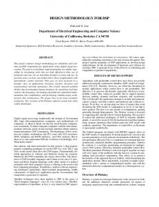
ES-676B. ATX form factor motherboard for Intel P4 socket 478 CPU with a. 400/
533MHz ... One floppy disk drive connector supports up to 2.88MB. - Integrates ...
Digital signal processing (DSP) applications involve processing long .... memory requirements that are imposed by multirate ..... Note that the problem we.
May 1, 2006 - and 12% area decrease using a 6,2 ALM comparing to a standard 4-LUT based logic module on the same process technology and routing ...
A Lean FPGA Soft Processor Built Using a DSP Block. Hui Yan Cheah 1, ... 2. RELATED WORK. There is a wide body of work on soft processors for FPGAs.
coding: |A1 - A2| + |B1 - B2| + |C1 - C2| + |D1 - D2|. ... 2 depicts the half-DSP block used in Altera's Stratix .... 2:1 multiplexors per 9x9-bit PPG is required to make the PPG ..... pr. 11..9], B[8..0]) and PPG(B[11..9], A[11..3]) aper, the FPCT h
MOTIVATION. Digital signal processing, traditionally the domain of Government ... multirate signal processing applications. Asynchronous ... Applications to multirate signals process- ... Note, however, that vectors and arrays have always been.
Oct 5, 2008 - The paper is organized as follows: the 3G requirements, advanced technologies that involve DSP, architecture examples and conclusions.
to 8 dimensions of Quaternion CORDIC algorithms, offered by J.M. Delosme and S.F.. Hsiao. This leads to significantly reduced computations in contrast to 8-D ...
28 Sep 2012 ... DSP Geografi Tingkatan 2 ... Kurikulum Geografi membolehkan murid
memahami fenomena .... Menyatakan perkembangan pengangkutan.
http://engineering.rowan.edu/~polikar/CLASSES/ECE404. Principles of
Biomedical. Systems & Devices. Lecture 19. Processing of Biological Signals ...
shown to be around 28 s, for patterns 16 character long, achieving a dramatic speed-up over classical FPGA computations. 2.2 Self-reconfiguration. The main ...
Objective: To compare remifentanil, alfentanil and fentanyl in providing analgesia for retrobulbar block injection. Methods: 69 patients were enrolled randomly ...
Keywords: Analgesia: Eye surgery; Anesthesia, Regional: Retrobulbar block; Remifentanil; Alfentanil; Fentanyl. Introduction. General anesthesia is hazardous in ...
tems that run 24 hours per day such as wireless base stations and server clusters ...... sumer devices,â in SDR Technical Forum, Orlando, Fla, USA,. November ...
Digital signal processing (DSP) software development has traditionally concentrated on ... mobile phone networks and future wireless local area networks.
TI assumes no liability for applications assistance, customer product design,
software ... This document presents a solution to control a permanent magnet.
This system runs in real-time on a laptop computer and performs image decimation (top row), contrast and brightness equalization (second row), inversion and ...
Use of a term in this book should not be regarded as affecting the validity of any
..... Award-winning technical support and DSP services enable you to bring ...
yThis research was supported in part by the NSF under grant MIP 95-01006. zThis research was supported in part by the William D. Mensch Jr. Fellowship. 1 ...
of original multi-parameter instrumentation for power quality assessment are ... Keywords: power quality, transients, wavelet transform, digital signal processors.
AbstractâThis paper describes a low-power DSP architecture for use in cochlear ... Lastly, non-overlapping bi-phasic pulses are generated and delivered ...
DSP's for wireless communications ... Wireless communications (baseband
processing) ..... Combined with a base station architecture and signal processing.
Aug 15, 2009 - optical polarization-diversity receivers in single-carrier systems. ..... RZ-pulse shaping with the constraint of a minimum estimation error.
In the Name of Allah, Most Gracious, and Most Merciful,. To my parents ... I would like to thank my advisor, Professor Earl E. Swartzlander, Jr. for his guidance ...
TURE is extended to exploit the fracturable multiplier unit incorporated in the DSP ..... 1 clock cycle less than Karatsuba-Ofman algorithm [7], while utilizing the ...
Circuits Syst Signal Process manuscript No. (will be inserted by the editor)
Abstract Multi-context architectures like NATURE enable low-power applications to leverage fast context switching for improved energy efficiency and lower area footprint. The NATURE architecture incorporates 16-bit reconfigurable DSP blocks for accelerating arithmetic computations, however, their fixed precision prevents efficient re-use in mixed-width arithmetic circuits. This paper presents an improved DSP block architecture for NATURE, with native support for temporal folding and run-time fracturability. The proposed DSP block can compute multiple sub-width operations in the same clock cycle and can dynamically switch between sub-width and full-width operations in different cycles. The NanoMap tool for mapping circuits onto NATURE is extended to exploit the fracturable multiplier unit incorporated in the DSP block. We demonstrate the efficiency of the proposed dynamically fracturable DSP block by implementing logic-intensive and compute-intensive benchmark applications. Our results illustrate that the fracturable DSP block can achieve a 53.7% reduction in DSP block utilization and a 42.5% reduction in area with a 122.5% reduction in power-delay product without exploiting logic folding. We also observe an average reduction of 6.43% in power-delay product for circuits that utilize NATURE’s temporal folding compared to the existing full precision DSP block in NATURE, leading to highly compact, energy efficient designs. Keywords Fracturable DSP · Temporal logic folding · NATURE architecture · Baugh-Wooley Multiplier R. Warrier E-mail: [email protected] S. Shreejith E-mail: [email protected] W. Zhang E-mail: [email protected] C. H. Vun E-mail: [email protected] S. A. Fahmy E-mail: [email protected] 1 2
School of Computer Science and Engineering, Nanyang Technological University, Singapore Department of Electronics and Computer Engineering, Hong Kong University of Science and Technology, Hong Kong 3 School of Engineering, University of Warwick, United Kingdom
2
Rakesh Warrier1 et al.
1 Introduction Multi-context reconfigurable platforms like the NATURE architecture [14] aim to extend the applicability of reconfigurable architectures by providing methods for fast context switching with minimal resource overheads and energy penalty. NATURE employs Temporal Logic Folding (TLF) at a fine-grained level, with distributed nano RAMs that enable reconfiguration of LookUp Tables (LUTs) to be achieved in a few picoseconds, much faster than commercial Field Programmable Gate Arrays (FPGAs). NATURE also supports reconfiguration of coarse-grained DSP blocks [11] and block RAMs (BRAMs) at similar speeds, making high frequency context switches feasible to improve area utilization and energy efficiency. The custom mapping tool, NanoMap [15], maps a circuit netlist to the architecture and generates the context switching controls automatically for each occupied logic element (LUTs, DSPs, and others), which together describe the circuit. Register Transfer Level (RTL) code can utilize mixed precision and custom datapath widths to achieve required accuracy and performance, but in NATURE these are seldom translated efficiently to hard-blocks like DSPs. The fixed precision on these hard DSP blocks often results in sub-optimal utilization, especially in cases where the data-widths are half the input width of the DSP block. In such scenarios, the NanoMap tool infers a complete DSP block but does not utilize the upper bits for computation, resulting in resource and power wastage. Variable precision DSP blocks have been described in academic research [8, 9] and implemented by commercial vendors (Altera) [1]. These support different computational precision and re-use of resources. The DSP blocks in Xilinx FPGAs offer dynamic programmability, that allows their function to be altered at run-time using special control inputs, improving their flexibility, as shown in [3] where they are used in the execution unit of a soft-processor. However, the compute precision of these DSP blocks cannot be altered across clock cycles, preventing them from being reused efficiently in a mixed precision circuit implementations, specifically on multi-context architectures that support TLF. Further, commercial FPGA tools do not currently automatically reuse DSP blocks in this manner, resulting in inefficient implementation in terms of area and power consumption [10]. In this paper, we present an enhanced DSP block architecture for NATURE that natively supports run-time precision selection and TLF. The proposed DSP block can switch between sub-width operation mode (2 independent 8×8 operations simultaneously), full width operation mode, or wider multiplication mode (32×32, 24×16, and 24×8 on a single DSP block) at runtime. The NanoMap tool is also extended to efficiently map multi-precision arithmetic operations on to the NATURE architecture that incorporates the proposed DSP block. Compared to a fixed precision reconfigurable DSP block, our experiments show that the proposed architecture results in a 63.5% and 76.2% reduction in power consumption and area while handling two half-width operations (in the same clock cycle) and 75% and 68.2% reduction in DSP block utilization with up to 122.5% reduction in power-delay product (P-D) across different benchmark circuits. We also observe that combining TLF with variable precision in DSP block computation provides significant advantage in (effective) area (1.24×), compared to a high-end Altera Stratix V device that incorporates variable precision DSP blocks. The proposed DSP architecture uses 16-bit operands to comply with NATURE architecture; however, the method can be extended to a 32bit DSP block that can simultaneously support two 16-bit operations or four 8-bit operations.
2 Background and Related Work NATURE is a hybrid reconfigurable architecture that can facilitate high-speed low-overhead dynamic reconfiguration [14]. The Logic Block (LBs) in NATURE are arranged island-style, connected by reconfigurable routing interconnect. High density, high speed nano RAMs are distributed in the logic fabric to store configuration bits. The ability to reconfigure NATURE every few clock cycles leads to the concept of TLF. TLF improves the logic density and area utilization by folding the logic circuit in time and maps each fold onto the same logic. Different folding levels
Fracturable DSP Block for Multi-Context Reconfigurable Architectures
3
are supported by NATURE, achieving different area/delay characteristics and offers significant flexibility in exploring area-delay trade-offs. For efficient mapping of applications onto NATURE, a design automation tool called NanoMap is used. It performs implementation of a circuit from RTL level to physical level through multiple steps: logic mapping, temporal clustering, temporal placement and routing, to generate configuration bits. After identifying the best folding level based on the design constraints and optimization objectives, LUT and DSP operations are scheduled using Force Directed Scheduling (FDS). Temporal clustering of LUTs and DSP blocks is performed to simplify the placement and routing, which is achieved using a customized version of the Versatile Place and Route (VPR) [2] tool that supports temporal folding. Direct links are incorporated in VPR to cascade DSP blocks and to route short-distance nets between LBs. The current fixed-precision DSP block [11] incorporated in the NATURE architecture is composed of two 16-bit pre-adders, a 16-bit Wallace tree multiplier and a 32-bit ALU unit that can perform addition, subtraction, 16-bit barrel shifting, and bitwise logical operations. The submodules form each stage of the three stage pipeline in the DSP block, which also incorporates multiple output registers to store the final result. Multiplexers within the datapath of the DSP block direct data from/to various stages, allowing numerous combinations of operations to be implemented on a DSP block. The DSP block operates with a fixed word length of 16-bits, which results in large wastage when the operands are half-width (8-bytes) or lower. Modern commercial FPGAs use highly advanced DSP blocks for accelerating complex computations. Xilinx’s 7-series FPGAs use the DSP48E1 architecture [12], that features an asymmetric multiplier design (25 × 18) with fixed precision and a maximum operating frequency of 741 MHz. DSP48E1 blocks also offer dynamic programmability that allows their function to be altered at run-time using control inputs, allowing them to be used flexibly. An example case is shown in [3], where a DSP48E1 block forms the execution unit of a highly efficient soft-processor. Altera’s variable precision DSP block can perform multiple sub-width operations concurrently (up to 3 9 × 9) with a design-time decision, while also featuring extensions like coefficient memory for efficient implementation of filters [1]. The literature also describes DSP block architectures from academic research with feature enhancements for supporting multi-input addition and varied bit-width multiplications [8, 9]. However, these DSP block architectures are primarily designed for single-context FPGAs and hence do not support logic folding.
3 Architecture of Fracturable DSP block 3.1 Fracturable Baugh-Wooley (BW) Multiplier with HPM Reduction Tree Parallel multipliers like the BW multiplier operate in three steps: generation of primary partial products, compression, and final addition. To compute two sub-multiplications in parallel, we introduce a fracturing mechanism at the primary Partial Product (PP) generation stage of a 16bit multiplier, as shown in Fig. 1. The fracturing mechanism uses configurable gates in addition to regular AND/NAND gates that are used in generic PP generation, with dynamic configuration bits that allow their functionality to be altered on a per-cycle basis. The multiplier unit uses two configuration bits, mode and gate, to determine the mode of operation. An alternative scheme would be to use independent and isolated PP generation stages for the full bit-width and half bit-width cases; however, this requires duplication of the PP stages and wide multiplexers for selecting the active datapath, resulting in larger area overhead, higher power consumption, and lower operating speeds. In the proposed scheme, a pipeline stage is introduced within the architecture to reduce the critical path, resulting in higher operating frequency over the existing DSP block in NATURE. The pre-adder and ALU stages of the DSP block hav been enhanced to support extended fractured operations like pre-add multiply or multiply-accumulate. As mentioned, the proposed architecture makes use of other building blocks to generate the PPs. These are the configurable AND/NAND, Gated-AND, Gated-NAND, Mode-based-
Rakesh Warrier1 et al.
4 Upper-8
Lower-8
Yin PP
Xin
PP/‘0’ GATE
Legend: PP
AND:PP AND/NAND:PP/PP
PP PP
Gated-AND:PP/‘0’
PP/‘0’
PP PP/PP
GATE
Gated-NAND:PP/‘0’
MODE Gated-Mode-NAND:(PP/M)G Mode-AND: PP/M
PP (PP/M)G
MODE
Final-Adder:FA
GATE Mode-Invert:FA/FA Pout Mode-Mux:FA/PP Upper-16
Lower-16
Fig. 1 Proposed fracturing mechanism of the 16-bit BW Multiplier.
Gated-NAND (Gated-Mode-NAND), XOR (Mode-Invert), Mode-OR-AND (Mode-AND), and 1-bit multiplexers (Mode-Mux). For the lower 16-bit partial products, the structure resembles an 8 × 8 multiplier, with additional rows above and below the regular 8-bit PPs. The partial products are generated by regular AND gates and configurable AND/NAND gates, while the Gated-AND/NAND gates are selectively disabled to allow sub-computations to be performed in isolation. The upper 16-bit PPs also mirror a similar structure operating on the upper 8 × 8 partial products. Here, the partial products are generated by Gated-AND, Gated-NAND, while the Gated-Mode-NAND generates logic ‘1’ to enable proper combination within the reduction tree. By generating the PP in this manner, we allow the logarithmic reduction tree to be reused for all modes of operation, without requiring any changes to its internal structure, reducing the area overhead incurred. The output of reduction tree is pipelined (single-stage) to limit the critical path within the multiplier. The configuration bits mode and gate determine the three operating modes of the multiplier at any given time. These can be automatically generated by our tool flow (see 3.2) for altering mode at run-time. We describe the operation of the circuit in the different modes below. Regular 16-bit mode: This mode is selected when gate is set to ‘1’ and mode is set to ‘0’. In this case, our circuit falls back to the regular 16 × 16 partial product tree, whereby the Gated-AND/NAND and Mode-based-Gated-AND/NAND compute regular AND/NAND functions respectively resulting in normal 16×16 partial products, which are then fed to the reduction tree and further to the final adder to compute the product. Dual 8 × 8 mode: This mode is selected when gate is set to ‘1’ and mode is set to ‘1’. In this scenario, the lower 8-bits of the inputs X and Y are taken as the input to the lower-16 section while the upper 8-bits of inputs X and Y are taken as inputs to the upper-16 section. With this configuration chosen, the Gated-AND/NAND computes regular AND/NAND operation, while the Gated-Mode-NAND gates are forced to value ‘1’. The configurable AND/NAND operates as a NAND gate, while the Mode-AND chooses the value of ‘1’. This generates two isolated sections of partial products which are then compressed using the HPM reduction tree. The Gated-ModeNAND gates ensure that the sign bits of the lower-16 bits are unaffected (and contained) during HPM reduction, while allowing the compression of the upper-16 bits in isolation. At the final adder stage, the multiplexers (Mode-Mux) choose the lower bit of the upper-16 reduced PP, while the Mode-Invert preserves the sign bit of the lower-16 result. Single 8 × 8 mode: This mode is selected when gate is set to ‘0’ and mode is set to ‘1’. In this scenario, the lower 8-bits of inputs X and Y are taken as the input to the lower-16 section while the upper 8-bits of inputs X and Y are ignored. With this configuration chosen, the GatedAND/NAND are completely gated in addition to the Gated-Mode-NAND gates, producing an output value ‘0’. This gating allows a significant power reduction when the multiplication is limited to a single 8-bit scope, compared to a regular 16-bit structure operating on 8 bits. As
Fracturable DSP Block for Multi-Context Reconfigurable Architectures
5 32
C
Eout
16 Pre-add/sub ± ±
A
16
Multiplier
×
32
±
×
±
P
ALU B
16 Register
±
1
±
Cout
Pre-add/sub D
16
32 Ein
1 Cin
Fig. 2 A 16-bit Enhanced DSP architecture. cycleE4
with the fractured mode, the configurable AND/NAND operates as a NAND gate, while the Mode-AND chooses the value of ‘1’. Thus by controlling the mode and gate pins at run-time, the multiplier enables computation of one 16 × 16 or two 8 × 8 in full mode, or a single 8 × 8 multiplication with reduced power consumption. DSP Block Architecture: To make effective use of our fracturable computational path, we have also defined an enhanced DSP block architecture, based on the architecture in [11]. Fig. 2 shows the basic block diagram of our enhanced DSP block. From the previous DSP block design, the modified DSP block contains gate, and mode pins to reconfigure the BW multiplier in different modes. The selection signals of these control pins are controlled by the multiple configuration bits stored in the associated configuration memory. Also, the interleaved multiplexers allow flexibility to realize different operations to be implemented using this basic structure. The two pre-adders (16-bit each) and the ALU (36-bit) have also been fractured using the same gate and mode inputs, allowing four 8-bit add/sub or two 16-bit ALU operations to be performed in addition to sub-width multiplication(s). The modified DSP block can now compute a wider range of computations on 8-bit operands than a standard non-fracturable DSP block, and this flexibility will be explored by our enhanced NanoMap tool. Supporting wider multiplications Using TLF, a 32 × 32 multiplication can be mapped using a single proposed DSP block in eight clock cycles. The 32-bit operands are separated and fed as the 16 least significant bits followed by the 16 most significant bits over multiple cycles. The partially computed results are stored in the intermediate registers for successive computations. The ALU perform shift and add operations on multiplier output to generate accurate results. Fig. 3 shows a 32-bit multiplier using only one DSP block using logic folding. Using a similar approach, the proposed DSP block can also implement 24 × 16 and 24 × 8 multiplications by
Rakesh Warrier1 et al.
6 Table 1 Power, area and frequency of the proposed DSP block. Design
Cell Area (µm2 )
Dynamic Power(µW)
FMax
One 8×8 Two 8×8 Full 16×16 (MHz)
Non-Fract. DSP
12938
934
1864
1160
333
Fract. DSP
14683
955
1140
1191
400
reconfiguring one DSP block. Moreover, this approach of realizing wider multiplication takes 1 clock cycle less than Karatsuba-Ofman algorithm [7], while utilizing the DSP block more efficiently. While folding can be explored for low-power designs, wider multipliers (like 32 × 32 or higher) in high performance designs can be implemented using the Karatsuba-Ofman algorithm by chaining DSP blocks. DSP Interconnect NATURE uses an island style architecture with each column implementing a single type of basic block. DSP blocks are placed along DSP columns, with direct links to top and bottom neighbours for cascading and chaining. The I/O ports of the DSP blocks are equally distributed on the left and right sides of the block, while the carry ports are located on the top and bottom sides. The I/O ports interface to the generic routing structure (via the switch matrix) to provide connectivity between DSP and SMB blocks. Including the input switch matrix, the proposed DSP block occupies an area equivalent to 6 SMB tiles.
3.2 Enhanced NanoMap In Section 2, we introduced the NanoMap design automation tool-flow that maps applications onto the NATURE architecture, including fixed precision DSP blocks. Here, the logic mapping step assigns arithmetic operations with operand bit-width greater than or equal to 8-bits to DSP blocks, while conditional operations and lower-width arithmetic operations are mapped onto LUTs. Multiple DSP blocks are automatically invoked when the operand bit-widths are wider than 16-bits. Once all nodes in the circuit are mapped using the library modules (LUTs, DSP blocks or Block Memories), FDS schedules the LUT and DSP operations into the best clock cycle. Further, the LUTs and FFs are packed into CLBs using a constructive algorithm. Our tool-flow enhances this packing algorithm to reduce DSP block utilization by exploiting the fracturable nature of the proposed DSP block. After mapping the mathematical operations to individual DSP blocks, the algorithm iteratively searches for operations that are scheduled in the same clock cycles. If any two DSP blocks perform sub-width operations (for example multiple 8 × 8 multiplication) in the same clock cycle, the algorithm groups them onto a single physical DSP block. Furthermore, the DSP operations scheduled in different cycles are also clustered together considering the connectivity and time span of the scheduled computation (or lifetime of the DSP). Non overlapping DSP operations with higher interconnectivity are clustered together for sharing in different cycles. This two-step approach allows a single DSP block to be reconfigured across cycles to implement sub-width (one 8 × 8 or two 8 × 8) full-width (one 16 × 16), or wider (24 × 16 or 32 × 32) operations, reducing the DSP block utilization, area, and power consumption. The placement and routing has also been modified to accommodate the fracturable nature of the primary inputs/outputs of the DSP blocks.
4 Area/Power overhead of Fracturable DSP Block and Performance Benefits To evaluate the area/power overhead and the reduction in frequency due to the increased logic in the multiplier unit, we synthesized our proposed DSP block unit using Synopsys Design Compiler targeting the TSMC 65nm cell library. For comparison, we also synthesized the existing NATURE
Fracturable DSP Block for Multi-Context Reconfigurable Architectures
7
Table 2 Resource comparison of benchmark circuits implemented on NATURE (with fracturable DSP block and with non-fracturable DSP block) for folding level-0 and an Altera Stratix V 5SGSMD4E1H29C1. Existing DSP With Fract. DSP % Reduction A×D P×D Benchmark (no of mult/mac, add/sub ops) DSPs Min. Period DSPs LUTs AEff Min. Period DSP Area Gain Gain DCT (13,19) ARF (16,12) FIR1 (11,10) FIR2 (8,15) Wavelet (10,14) ASPP4 (3,4) EWF (8,26) HAL (6,4) Paulin (2,2) HornerBezier (8,3) MotionVector (12,12) MatrixMult (48,12) Smooth Triangle (17,20)
DSP block which uses a standard BW multiplier, with the same target library. The results are shown in Table 1. The Table compares the resource consumption of the proposed DSP architecture against the existing (non-fracturable) DSP block in NATURE [11], which uses a wallace tree multiplier, with a maximum operating frequency of 333 MHz. It can be observed that the proposed DSP architecture, based on the BW multiplier with an HPM reduction tree, incorporates multiple operating modes (as discussed in sec. 3) and deep pipelining in the final adder stage, thus attaining a higher operating frequency of 400 MHz with a 13.4% increase in cell area. We also estimate the power consumption of the proposed DSP block using the Synopsys PrimeTime tool, the results of which are also shown in Table 1. The power (switching power) measured using Synopsys primetime compiler consists of Power total = Net Switching Power + Cell Internal Power +Cell Leakage Power , where the net switching power is the power estimated using the switching activity values generated using a VCD dump file, the cell internal and leakage power are the values corresponding to each standard cell of the library module that is being used. We observe that with fracturing, our architecture results in a 38.3% reduction in power and 43.8% reduction in area when two 8-bit multiplications are scheduled in parallel, which would utilize two 16-bit multipliers in the NATURE architecture. For single 8-bit and full precision modes, operating at 400 MHz results in a slight increase in power consumption of 2% and 2.67% respectively over the current NATURE DSP block that runs at 333 MHz. At 333 MHz, we observed that the fracturable design consumes 15% less power for both single 8-bit and full precision operations, compared to the existing DSP block. Thus we see a clear advantage in terms of performance and power consumption for the proposed DSP block architecture in mixed precision digital circuits, which are commonly used in many applications like audio, vision systems and others. We further quantify these advantages in the case of actual circuits in the section below.
5 Performance Results and Discussions For our experiments, we have used generic RTL/netlists of circuits including Discrete Cosine wave Transform (DCT), Auto-regression Filter (ARF), Application-Specific Programmable Processor (ASSP4) [4], Greatest Common Divisor (GCD), Differential-equation solver (Paulin) [6], Wavelet Transform, and Finite Impulse Response filters (FIR1 and FIR2). In addition to these generic circuits, we have also evaluated the proposed DSP using complex functions such as the Elliptical Wave Filter (EWF), HAL, Smooth Triangle, HornerBezier, Motion Vector, and Matrix Multiplication, starting from their RTL/netlist description. We set the input precision to 8-bit for all evaluations.
8
Rakesh Warrier1 et al.
In the experiments, we explore two folding levels (0 and 1) and evaluate the area-delay (A-D) and power-delay (P-D) trade-offs (total runtime power) achieved using the proposed fracturable DSP block compared against the existing NATURE DSP block. We also compare the results of folding level 0, which can be considered equivalent to a single context FPGA, against the results on an Altera Stratix V (5SGSMD4E1H29C1) device that features 6-input fracturable LUTs and variable precision DSPs, as shown in Table 2. To account for the difference in platforms, we compute the effective area utilized by the implementation (in terms of equivalent LUTs) using the relation AEff = LUT Max /DSP Max ∗ DSPutilization + LUTutilization [13]. Also, the number of multiply/MAC and add/sub operations in each benchmark is shown (in brackets), which helps determine the reduction in DSP blocks achieved by exploiting their fracturable nature (on Stratix V and on the proposed DSP block in NATURE). It can be observed from Table 2 that the proposed DSP block achieves a significant reduction in DSP utilization compared to the existing fixed precision DSP block architecture in NATURE. This is because the two sub-width mult/MAC or add/sub operations that are scheduled in the same clock cycle, can be merged into a single (proposed) DSP block by altering the mode and gate configuration bits, while this requires two DSP instances with the existing architecture. Also, Table 2 shows that the % reduction in DSP block utilization is significant for the benchmark circuits with acyclic dataflow graphs (FIR1, FIR2, Motion Vector, EWF, ARF etc.), since these circuits contain only sequences of arithmetic operations that can be scheduled to their best folding cycles. This results in better merging of non-overlapping arithmetic nodes onto the same fracturable DSP block(s). Finally, the ASSP4 benchmark shows negative gain in area, since the cyclic circuit contains only one arithmetic node that can be merged, and the area penalty of the fracturable DSP block (13.4% over the existing DSP block) cannot be covered by this limited merging. An average reduction of 53.7% in DSP block utilization, 42.5% in area, and 122.5% in P-D product across all benchmarks is achieved. Compared to the implementation on Altera Stratix V device, which maps only mult/MAC operations onto DSP blocks while add/sub operations are implemented using LUTs, we observe a 1.24× average reduction in effective area (across all benchmarks), despite the Altera device having superior LUTs (6-input fracturable v/s 4-input fixed on NATURE) and DSP blocks (3 9 × 9 v/s 2 8 × 8 for proposed DSP on NATURE) architecture. It can also be observed that the Quartus tool automatically merges sub-width operations to reduce DSP block utilization in multiple benchmarks (DCT, ARF, PAULIN); however, our enhanced NanoMap tool-flow is able to further reduce the DSP block utilization by exploiting the fracturable Pre-add/sub and Post-add/sub blocks in the proposed DSP block. Table 3 shows the mapping results of the benchmark circuits on NATURE architecture with the proposed DSP blocks and on NATURE with fixed precision DSP blocks at folding level 1. In folding level 1, the logic is folded (reconfigured) at a depth of 1 LUT computation. Here, apart from combining two 8-bit multipliers scheduled in same clock cycle to a fractured DSP block, it can be reused across clock cycles to implement subsequent operations if there are no resource conflicts. Further, each DSP block may vary its configuration from full 16×16 mode to the powersaving single 8×8 mode or a fractured dual 8×8 mode across different cycles, as determined by its configuration bits. This flexibility allows further optimizations in resource consumption, compared to folding level 0, which was discussed earlier in Table 2. For each benchmark, we observed that the overall resource consumption was reduced in folding level 1, with both the fixed precision DSP block based NATURE and the proposed DSP block based NATURE. Shown in Table 3 are the 6 benchmarks which offer reduced resource consumption between the two target platforms (NATURE with fixed precision DSP block and NATURE incorporating proposed DSP block). In the case of the smaller benchmarks (FIR1, FIR2 and others), we observe that temporal folding introduces resource conflicts, limiting the scope of DSP reuse through fracturing. We observe an average reduction of 17.5% in DSP block utilization across the 6 benchmarks and an average A–D improvement of 1.1× for the NATURE architecture that incorporates our proposed DSP block. We also observe a P-D product reduction of 6.43% across the benchmark circuits over the NATURE architecture with fixed precision DSP block.
Fracturable DSP Block for Multi-Context Reconfigurable Architectures
9
Table 3 Resource comparison of benchmark circuits implemented on NATURE (with fracturable DSP block and with non-fracturable DSP block) for folding level-1 and on FDR 2.0. Non-Fracturable DSP Fracturable DSP A×D P×D Benchmark Wavelet ASPP4 Paulin Motion Vector MatrixMult Smooth Triangle
DSPs 9 3 4 6 23 10
Min. Period 3.88 3.57 3.67 3.62 3.69 3.65
ns ns ns ns ns ns
FDR 2.0
DSPs Min. Period Gain Gain DSPs Min. Period 8 2 3 5 21 9
3.14 ns 3.68 ns 3.4 ns 3.01 ns 3.58 ns 3.36 ns
1.23× 1.16× 1.21× 1.27× 1.01× 1.07×
1.16× 1.01× 1.08× 1.15× 1.03× 1.02×
17 5 4 12 30 22
4.28 3.88 3.67 3.81 3.78 3.91
ns ns ns ns ns ns
% Reduction A×D DSP
Gain
52.9 60.0 25 58.3 30 59
2.56× 2.29× 1.52× 2.38× 1.17× 2.11×
We also compare the results of NATURE with the fracturable DSP block against the FDR 2.0 architecture [5] that incorporates a DSP block with 3 pipeline stages. Compared to the fixed precision DSP block available on the FDR architecture, the fracturable nature of our DSP block enables the mapping tool to merge more DSP operations on to the same DSP block. This results in improved area and power gain over the existing FDR architecture over the set of benchmarks, as shown in Table 3. We observe an average reduction of 47.7% in DSP block utilization across 6 benchmarks and an average A-D improvement of 2.01× for the fracturable DSP incorporated NATURE over FDR architecture. For more computationally intensive circuits, we believe that the proposed DSP block can result in a more significant improvement in energy efficiency without compromising system performance. Finally, it is worth mentioning that though we have used NATURE as a platform to demonstrate the capabilities of our fracturable DSP block, it could also be integrated into FDR 2.0 to extract similar gains in resource and energy consumption.
6 Conclusion In this paper we proposed a fracturable DSP block architecture for improving energy efficiency of computations on the multi-context FPGA architecture, NATURE. The proposed DSP block achieves this efficiency by fracturing its internal compute-path while maintaining the capability to dynamically switch computational precision. By utilizing this capability, our proposed DSP block can efficiently handle two independent half-width (8×8) multiplications in complete isolation, perform a single 8×8 multiplication with lower power consumption, or operate on regular full-width 16-bit operands. Furthermore, these modes can be switched dynamically, allowing efficient reuse of the DSP block for low-power applications. We have extended the NanoMap tool flow to efficiently map and merge mixed precision multiplications on the proposed DSP block. Experimental results show that mapping benchmarks circuits onto the NATURE architecture with this proposed DSP block achieved 42.5% and 53.7% average reduction in area and DSP block utilization with 122.5% reduction in P-D product without utilizing temporal folding (folding level 0). We also observe improvements in energy efficiency and resource utilization when temporal folding is employed, without sacrificing performance. We aim to evaluate a 32×32 DSP block that can support two half-width (16-bit) or four quarter-width (8-bit) operations simultaneously, and extend the tool-flow to support these enhancements.
References 1. Altera Inc.: Variable Precision DSP blocks in Stratix V devices (2013) 2. Betz, V., Rose, J.: VPR: A new Packing, Placement and Routing Tool for FPGA Research. In: Proc. Int. Conf. on Field-Programmable Logic and Applications (FPL), pp. 213–222 (1997)
10
Rakesh Warrier1 et al.
3. Cheah, H.Y., Brosser, F., Fahmy, S.A., Maskell, D.L.: The iDEA DSP Block Based Soft Processor for FPGAs. ACM Transactions on Reconfigurable Technology and Systems 7(3) (2016) 4. Ghosh, I., Raghunathan, A., Jha, N.K.: Hierarchical Test Generation and Design for Testability Methods for ASPPs and ASIPs. Tran. on Computer-Aided Design of Integrated Circuits and Systems 18(3), 357–370 (1999) 5. Lin, T.J., Zhang, W., Jha, N.K.: FDR 2.0: A Low-Power Dynamically Reconfigurable Architecture and Its FinFET Implementation. IEEE Transactions on Very Large Scale Integration (VLSI) Systems 23(10), 1987–2000 (2015) 6. Lingappan, L., Ravi, S., Jha, N.K.: Satisfiability-Based Test Generation for Nonseparable RTL controller-Datapath Circuits. Tran. on Computer-Aided Design of Integrated Circuits and Systems 25(3), 544–557 (2006) 7. Machhout, M., Zeghid, M., Youssef, W.E.H., Bouallegue, B., Baganne, A., Tourki, R.: Efficient large numbers karatsuba-ofman multiplier designs for embedded systems. International Journal of Electrical, Computer, Energetic, Electronic and Communication Engineering 3(4) (2009) 8. Parandeh-Afshar, H., Cevrero, A., Athanasopoulos, P., Brisk, P., Leblebici, Y., Ienne, P.: A Flexible DSP Block to Enhance FPGA Arithmetic Performance. In: Proc. of Int. Conf. on Field-Programmable Technology (FPT), pp. 70–77. IEEE (2009) 9. Parandeh-Afshar, H., Ienne, P.: Highly Versatile DSP Blocks for Improved FPGA Arithmetic Performance. In: Proc. of Int. Sym. on Field-Programmable Custom Computing Machines (FCCM), pp. 229–236. IEEE (2010) 10. Ronak, B., Fahmy, S.A.: Mapping for Maximum Performance on FPGA DSP Blocks. IEEE Transactions on Computer Aided Design of Integrated Circuits and Systems 35(4), 573–585 (2016) 11. Warrier, R., Hao, L., Zhang, W.: Reconfigurable DSP Block Design for Dynamically Reconfigurable Architecture. In: Proc. of Int. Symp. on Circuits and Systems (ISCAS), pp. 2551–2554 (2014) 12. Xilinx Inc.: UG369: Virtex-6 FPGA DSP48E1 Slice User Guide (2011) 13. Xu, S., Fahmy, S.A., McLoughlin, I.V.: Square-rich Fixed Point Polynomial Evaluation on FPGAs. In: Proc. Int. Sym. on Field-programmable Gate Arrays (FPGA), pp. 99–108. ACM (2014) 14. Zhang, W., Jha, N.K., Shang, L.: A Hybrid Nano/CMOS Dynamically Reconfigurable System - Part I : Architecture. ACM Journal on Emerging Technologies in Computing Systems (JETC) 5(4), 16 (2009) 15. Zhang, W., Jha, N.K., Shang, L.: A Hybrid Nano/CMOS Dynamically Reconfigurable System - Part II: Design Optimization Flow. ACM Journal on Emerging Technologies in Computing Systems (JETC) 5(3), 13 (2009)