www.nature.com/scientificreports
OPEN
Graphene Distributed Amplifiers: Generating Desirable Gain for Graphene Field-Effect Transistors
received: 29 October 2014 accepted: 03 November 2015 Published: 04 December 2015
Hongming Lyu1,3, Qi Lu1, Yilin Huang1, Teng Ma4, Jinyu Zhang1, Xiaoming Wu1, Zhiping Yu1, Wencai Ren4, Hui-Ming Cheng4, Huaqiang Wu1,2 & He Qian1,2 Ever since its discovery, graphene bears great expectations in high frequency electronics due to its irreplaceably high carrier mobility. However, it has long been blamed for the weakness in generating gains, which seriously limits its pace of development. Distributed amplification, on the other hand, has successfully been used in conventional semiconductors to increase the amplifiers’ gain-bandwidth product. In this paper, distributed amplification is first applied to graphene. Transmission lines phasesynchronize paralleled graphene field-effect transistors (GFETs), combining the gain of each stage in an additive manner. Simulations were based on fabricated GFETs whose fT ranged from 8.5 GHz to 10.5 GHz and fmax from 12 GHz to 14 GHz. A simulated four-stage graphene distributed amplifier achieved up to 4 dB gain and 3.5 GHz bandwidth, which could be realized with future IC processes. A PCB level graphene distributed amplifier was fabricated as a proof of circuit concept.
The irreplacably high carrier mobility of graphene has been of great interests to the elctronics community and motivated researcher to endeavor on graphene radio frequency (RF) electronic devices1–3. Graphene field-effect transistors are widely studied and many research groups have generated cutoff frequencies (fT) of hundreds of GHz4–9, with the record-high value of 427 GHz9. Poineering works on graphene circuits have led to the demonstration of frequency doublers10–12, ambipolor mixers13 and modulators14,15, in which graphene’s unique property of electron and hole symmetry is utilized. By superimposing an sinusoidal signal on the minimum conductance point (Dirac point), the electron or the hole branches, the frequency and phase of the output signal could be modulated. Another appliction, the graphene passive circuits (e.g. graphene resistive mixers)16–19, attracts more attentions and already shows potential to compete with conventional semiconductor technologies. The authors’ group has combined CMOS back-end-of-line (BEOL) processes and graphene to realize a two-layer-routing four-GFET double-balanced mixer IC, which generated IIP3 up to 21 dBm19. However, the overall progress in electronics is greatly hindered by graphene’s gapless band structure1,2. Obviously, the lack of drain current saturation is detrimental to amplifiers. In particular, even though the fT in various groups has reached hundreds GHz, the fmax of GFETs, representing the ability to generate power and voltage amplification, has halted at only 70 GHz5. Graphene researchers have tried conventional amplifier architectures. Andersson et al. utilized a matching surface mount inductor on the input gate to yield a return loss of 20 dB. Their work achieved S21 of 10 at 1 GHz20. Guerriero et al. fabricated graphene voltage amplifiers in complementary push-pull configuration, which generated a voltage gain of 11.4 dB and a − 3 dB bandwidth of only 70 kHz21. In a recent work, a three stage cascade amplifier
1
Institute of Microelectronics, Tsinghua University, Beijing, 100084, China. 2Tsinghua National Laboratory for Information Science and Technology (TNList), Beijing, 100084, China. 3Department of Electrical & Computer Engineering, University of California, San Diego, La Jolla, CA 92093, USA9. 4Shenyang National Laboratory for Materials Science, Institute of Metal Research, Chinese Academy of Sciences, Shenyang, 110016, China. Correspondence and requests for materials should be addressed to H.L. (email:
[email protected]) or H.W. (email:
[email protected]) Scientific Reports | 5:17649 | DOI: 10.1038/srep17649
1
www.nature.com/scientificreports/
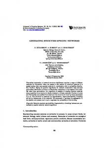
Figure 1. SEM and optical microscope images of the GFET. Cross section (a) and top (b) views of the GFET by SEM. Scale bars: 2 μm. (c) Optical microscope image of the GFET with probing pads.
IC achieved a gain of 4 dB at 4.8 GHz22. Despite these works, graphene’s application in amplifiers with conventional topologies are mostly disappointing. On the other hand, graphene’s IC process has witnessed substantial improvements12,19,22. Both Han et al. and the authors’ group have proposed the multi-layer-routing inverted process for graphene integration, which serves as the foundation for future novel graphene circuit architectures12,19,22. The inverted process utilizes CMOS BEOL processes to fabricate circuit and device structures, followed by CVD graphene transfer at the back end of the flow. This process utilizes existing CMOS technologies to the maximum extend and greatly reduces contaminations and potential damages to graphene. In this paper, the graphene distributed amplifer is proposed to solve its long-standing weakness in amplification. Engineers have successfully applied distributed amplication to conventional semiconductor technologies to increase the amplifiers’ gain-bandwidth-product23–26, which could not be increased simply by parallelizing transistors, because the increase in the transconductance is compensated for the corresponding increase in the input and output capacitances. The distributed amplifiers place transistors along artificial transmission lines, adding the gm of each transistor in a phase-synchronized manner. Therefore, the bandwidth-gain-product could be increased. While the gain of a conventional cascade amplifier is the product of the gain of each stage, distributed amplifiers’ gain is directly proprotional to the number of stages. This trait makes distributed amplification scheme especially suitable for graphene, as each GFET stage generates very modest or less-than-unity gains. The otherwise product of the gain of each stage would be mediocre. Four GFETs with gate lengths of 300 nm through 500 nm have been fabricated, which generated fT ranging from 8.2 GHz to 10.6 GHz and fmax 12.4 GHz to 16.6 GHz without de-embedding (Misallignment existed in this batch of devices, breaking the relationship between the fT and fmax metrics and the gate length). The fmax exceeded fT in these works due the low resistance of the buried gates5. Measured S-parameters of the GFETs were used in graphene distributed amplifier simulations. The circuit schematic employed artificial transmission lines formed by lumped inductors and capacitors to phase-syncronized each GFET stage. Simulations generated up to 4 dB gain and and 3.5 GHz bandwidth, which is the first graphene wide-band amplification dicussed in literature. These designs could be realized by IC technologies with precise models. However, at the present stage, a PCB-level distributed amplifer was fabricated. As individual GFETs and bonding wires were not precisely modeled, the passive components of any small values were avoided. Redesign of the passive components sacrificed the gain, while the bandwidth was maintained. The measured performance was in agreement with circuit simulations.
Results and Discussion
Graphene Field-Effect Transistors. GFETs in buried-gate structure have been fabricated. Cross-
section and top views of a 400 nm-gate-length GFET structure are shown in Fig. 1a,b, respectively. Chemical-mechanical-planarization (CMP) process flattened the wafer surface, which guarrenteed the successfulness of the following graphene transfer process. Cross section made by focused-ion-beam (FIB) indicated the thickness of the gate of 600 nm. Such thickness effectively lowers the gate series resistance, which is favourable from fmax point of view. The GFETs employed a two-finger structure with each finger 6 μ m wide. The gate dielectric employed HfO2 with equivalent oxide thickness (EOT) of 2 nm formed directly on the buried gate. Graphene was synthensized by CVD method and transferred by “bubbling” method as previously reported (details in Method)27,28. The channel of the GFETs was defined by contact photolithography and contacts by electron beam photolithography (EBL). The contacts were 40 nm Pt (details in Method). The probing pads were 80 μ m × 80 μ m with 100 μ m pitch in ground-signal-ground (GSG) layout, as shown in Fig. 1c. All devices have not gone through passivation step for convenience. Several reports have shown various dielectrics, such as Si3N429, BN30, Al2O331, etc., could effectively protect graphene devices. Future works should consider passivation to increase the stability and reliability of graphene Scientific Reports | 5:17649 | DOI: 10.1038/srep17649
2
www.nature.com/scientificreports/
Figure 2. RF Performance of the GFETs. fT and fmax of GFET #1 (a), GFET #2 (b), GFET #3 (c) and GFET #4 (d).
Figure 3. Schematic of a four-stage graphene distributed amplifier.
devices. S-parameters have been measured on chip up to 40 GHz under ambient atmosphere using Agilent N8230C network analyzer. Four GFETs labeled as GFET #1 ~ 4 featured gate lengths of 300 nm, 500 nm, 500 nm and 400 nm, respectively, and demonstrated fT/fmax of 8.2 GHz/16 GHz, 8.4 GHz/12.5 GHz, 9.1 GHz/12.4 GHz, 10.6 GHz/16.6 GHz, respectively, as shown in Fig. 2. These results were without de-embedding. The devices were then cut out of the chip with the probing pads which enabled wire bonding in following works.
Distributed Amplifiers. Figure 3 shows the schematic of a four-stage graphene distributed amplifier. Artificial transmission lines formed by lumped elements are periodically loaded with the gate and drain terminals of the GFETs, forming the so-called gate and drain transmission lines. An RF signal applied at the input end of the gate line travels down to the other end, where it is absorbed by the terminating impedance. The signals sampled by the gate of a GFET at a different location with different phases is transferred to the drain line. The two gate and drain transmission lines pocess the same phase velocity. Therefore, the gains of each stage are combined in the forward-travelling direction. The backward-traveling signal on the drain line is absorbed at the frontier end. As long as the gain per section is greater than the corresponding loss, the overall gain of a distributed amplifier can be increased even without limit. While the gain of conventional cascade amplifiers are the product of each stage, distributed amplifiers increases the gain proportional to the number of stages, which is especially attractive to graphene, since the otherwise multiplication could not generate satisfying gains. The four GFETs in the schematic are labeled as T1~4. Passive components, Cd, Cg, Ld and Lg, constitute the gate and drain artificial lines. R1 and R2 form the two terminating resistances. Circuit simulation based on measured S-parameters of the GFETs was performed in a standard circuit simulator, Agilent Advanced Design System (ADS). In Simulation #1, T1 through T4 all employed GFET #4, respresenting ideal situations when GFETs are exactly identical. The optimization was performed with three goals: 1) S21 > 5 dB; 2) S11