email: {dias, berry, jserot, marmoito}@lasmea.univ-bpclermont.fr. ABSTRACT ... sues are discussed and a template tracking application is given as example ...
HARDWARE, DESIGN AND IMPLEMENTATION ISSUES ON A FPGA-BASED SMART CAMERA Fabio Dias, Franc¸ois Berry, Jocelyn S´erot, Franc¸ois Marmoiton LASMEA - Laboratoire des Sciences et Mat´eriaux pour l’Electronique et d’Automatique Universit´e Blaise Pascal - 24 avenue des Landais - 63177 Aubi`ere - FRANCE email: {dias, berry, jserot, marmoito}@lasmea.univ-bpclermont.fr ABSTRACT Processing images to extract useful information in real-time is a complex task, dealing with large amounts of iconic data and requiring intensive computation. Smart cameras use embedded processing to save the host system from the low-level processing load and to reduce communication flows and overheads. Field programmable devices present special interest for smart cameras design: flexibility, reconfigurability and parallel processing skills are some specially important features. In this paper we present a FPGA-based Smart Camera research platform. The hardware architecture is described, and some design issues are discussed. Our goal is to use the possibility to reconfigure the FPGA device in order to adapt the system architecture to a given application. To that, a design methodology, based on pre-programmed processing elements, is proposed and sketched. Some implementation issues are discussed and a template tracking application is given as example, with its experimental results. Index Terms— Smart camera, embedded image processing, FPGA-based system, reconfigurable architecture, design methodology 1. INTRODUCTION Artificial intelligent systems often need to get information about the surrounding environment, in order to adapt their behavior or perform a given task. In much cases, the quality of extracted information determines system’s performance. Hence, the sensing system plays an important role in several applications, from intelligent vehicles (autonomous navigation, obstacle detection, assisted driving, etc.) and robotics (servoing) to security systems (surveillance, face and behavior recognition, etc.). Image sensors are frequently employed, alone, in network [1] [2], or in combination with other sensing devices through data fusion techniques [3]. Some interesting features presented by image sensors are their low-cost (huge choice of COTS devices), easy integration (standard interface protocols such USB or Firewire), and the ability to extract different kinds of information (motion
detection and estimation, localization, detection and recognition of a given pattern (face, object), etc.). However, many vision tasks exhibit the following characteristics: first, they rely on real-time operation to extract useful information from a dynamic environment. Second, they involve low-level, time consuming processing of large amounts of iconic data. They therefore place stringent constraints on the computing system, both in terms of communication bandwidth and computing power. Even with recent outstanding advances in microelectronics, standard PC architectures are frequently unable to deliver required performances for such applications. Embedded processing can help to solve these problems by executing low-level tasks within the camera platform, before data transmission to the host system. This way, amounts of data to be transmitted can be strongly reduced, and transmitted data is more pertinent than a raw pixel flow, meaning that received data can be promptly used by the host system, without pre-processing time consuming tasks. Processing resources are added to the camera’s hardware in form of FPGA devices [4], media/streaming processors [5], DSP’s, etc. Cameras with embedded processing resources are known as “Smart Cameras”, and are the subject of growing interest. Field programmable logic presents special interest for smart cameras design. Reconfigurability allows to adapt camera’s architecture for a wide palette of applications, and data and task parallelism can be easily and massively exploited to meet real-time constraints. Moreover, FPGA’s flexibility allows to interconnect different external devices (memories, ASICs), as well as internal soft-core processors, making possible to exploit mixed hardware/software solutions. However, the integration of such devices makes the application design and implementation processes more complex, as the heterogeneous nature of the system requires co-design techniques and tools. This paper discusses some implementation issues for embedded image processing on a FPGA-based architecture. It is organized as follows: in section 2, the hardware architecture of a FPGA-based smart camera is described. In section 3, a design methodology for fast prototyping is proposed. As part of this methodology, a window-based processing element for low-level image processing is presented in section 4. Finally,
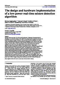
SENSOR 2 MB
2 MB @
2 MB
STRATIX EP1S60
@
@ data
data
@
2 MB @ data
Data
Sensing Devices Temp Acc XY Acc Z Gyro X Gyro Y Gyro Z
8 input ADC
64 MB
@ data
Global memory SDRAM
data
2 MB
SRAM Private memories
Lens
ADC
Fig. 1. Smart Camera research platform. in section 5, an embedded tracking application is presented to illustrate camera’s utilization, followed by some conclusions in the last section. 2. SMART CAMERA HARDWARE ARCHITECTURE We have designed and built a smart camera platform (figure 1) based on a CMOS image sensor and a FPGA device. The latter, an ALTERA Stratix EP1S60F1020C7 device, plays the central role in the system, being responsible to interconnect and control different hardware devices (image sensor, memories), and to handle the communication with the host system. Surrounding the FPGA, 10Mb (5x 1MWords) of SRAM and 64Mb of SDRAM are available for image and data storage. A synoptic diagram of the hardware architecture is shown in figure 2. The choice of a CMOS image sensor is justified by its random addressing capability. This feature is extremely useful when dealing with applications such as feature tracking, where WOI (window of interest) acquisition is needed. It allows to have a high-resolution sensor, while not delivering full resolution images all the time, which would be prohibitive due to time constraints of some applications. Random addressing makes possible to have high resolution images or high frame rates with the same sensor, and according to the application needs. A strength of this hardware platform is its modularity. Different hardware devices are integrated in different boards (except for memories, which share the same board as the FPGA). These boards are interconnected, and can be replaced to allow the platform’s evolution. Thanks to this feature, this smart camera platform has frequently evolved. The actual configuration features a 4Mpixels LUPA-4000 image sensor, from Cypress Semiconductors, and a Firewire Interface. An upgrade to integrate a FPGA device from the new Stratix 3 family is being considered. The LUPA-4000 image sensor can acquire up to 66Mpix-
Light
IEEE 1394 Imager addressing
UART
Communication
JTAG
HOST COMPUTER
Imager
Fig. 2. Smart camera hardware architecture (synoptic scheme). els per second, and full resolution format is 2048 x 2048, each pixel coded in 10 bits. Image capture is done in global shutter mode. The acquisition frequency allows a frame rate of more than 200frames/s in VGA mode (640 x 480). The IEEE 1394 interface offers a real (exploitable) bandwidth of 20Mbytes/s from the camera to the external environment (host system), and 10 Mbytes/s in the other direction. The hardware architecture also integrates an inertial sensing unit, with 2 2D accelerometers and 3 gyroscopes, allowing to estimate 3D ego-motion, camera orientation and camera position in real-time. A board containing a DSP device can also be connected to the system, communicating with the FPGA through a shared memory, and allowing to perform complex signal processing routines. 3. DESIGN METHODOLOGY Prototyping on heterogeneous architectures is a complex task. The application designer must deal with several programming models and languages (VHDL, C, C++, Assembler), and their respective development environments. Communication among processing modules of different natures (hardwired, programmable) must be managed, as well as tasks synchronization and data deployment. A design methodology would help to reduce implementation complexity and development time. The work presented here is part of an approach towards a design methodology for low-level vision applications on FPGAbased architectures. This methodology relies on a programming tool allowing to generate a suitable system architecture for a given programmed application. This architecture is obtained through reconfiguration of the FPGA, and is based on a programmable control module and a set of pre-designed configurable data processing elements (PE’s). The control module acts as the system supervisor, communicating with the processing elements through flags (handshake signals) and registers. It is responsible for data deployment and for configuring and synchronizing different PE’s.
Fig. 3. Schematic of a SoPC architecture illustrating the proposed methodological approach. These elements can be generic, as an Arithmetic Logic Unit (ALU), or specialized, as a Fast Fourier Transform (FFT) IP or a Finite Impulse Response (FIR) filter for instance. An analogy can be done with a microprocessor architecture, where the control module plays the role of instruction decoder, and the processing elements appear as specialized ALUs. Hardware drivers are also available in order to control and configure the external devices (as peripheral controllers in a µP ). These drivers are controlled by the control module itself (as the image sensor driver for instance), or directly by the PE’s (as the memory managing units (MMU), allowing direct memory access). Communication between different PE’s can be done means a direct link, or via a shared memory. Processing elements are able to handle scalar data, vectors or 2D matrices (image samples), which is the most natural data format when dealing with image processing. Figure 3 depicts an example of a System on Programmable Chip (SoPC) architecture, conceived according to the proposed design methodology. The control module disposes of a program memory, where the application program is stored. This program describes the task scheduling and data dependencies of the application, allowing the control module to activate, configure and synchronize different PE’s and external hardware devices. In the center of the figure, the “processing elements zone” may contain several PE’s. In the example, 6 PE’s are instantiated. PE1 performs a given operation on data coming from inertial sensors, while PE2 receives its input data from the image sensor. Results from these PE’s are used by PE3, which disposes of an internal memory, in order to store intermediate results for example. This memory can be reserved, or shared with another PE for data exchange. Results from PE3 are sent to PE6 via a direct link, while PE6 communicates with PE4 via a shared external memory. PE4 sends its results to the host system, through the interface driver. PE5 performs a given operation on the pixel flow, and its results are sent to the control module. Since all PE’s are connected to the control module, these connections are not shown in the figure. Parallelism can be exploited at the system level (multiple PE’s working simultaneously) or at the PE’s level, through a
SIMD PE for instance. Our final goal is to conceive an automatic designing tool, able to generate the architecture for the “processing elements zone” and its connections with the fixed part of the SoPC architecture (control module and external devices drivers). Using this tool, the application designer is supposed to program the control module behavior (task sequence), and through the analysis of the programmed code, a suitable SoPC architecture for his application is defined and generated. To that, a library containing a set of pre-designed PE’s is used. If necessary, new processing elements can be included in the library, but their design must fit a set of rules to ensure their compatibility with the rest of the system. In next section, a configurable PE able to deal with 2D matrices (image samples) is presented. It is an example of generic element which can be included in the PE library. The library can also contains specialized PE’s, as the SAD-based motion estimation module employed in section 5. 4. GENERIC WINDOW-BASED PROCESSING ELEMENT Low-level vision tasks frequently involve neighborhood operations, combining several adjacent pixels to produce a single result. As these operations are applied over a small defined portion of the input image, they are often called “Windowbased”. Some examples are convolution (spatial filters, wavelets), correlation estimation (SAD, SSD) and morphological transformations (dilatation and erosion). These operations deals with big amounts of data, performing repetitive computations over the whole image. Being time and processing expensive, the optimization of these processes is essential to meet temporal performances imposed by the real-time constraint. Hence, from the point of view of the proposed design methodology, a configurable window-based operator [6] is a useful PE to be included on the library. The operator proposed here is based on the computational model presented in [7]. This model supposes that a windowbased operation is performed between two image operands A(i,j) and B(i,j) , of size n × n, and producing an image result Q(i,j) , size n × n, or a scalar result x (eqs. 1 et 2). Q(i,j) = FM (FD (A(i,j) , B(i,j) ))
(1)
x = FR (Q(i,j) )
(2)
Q(i,j) is obtained through successive application of functions FD and FM . Function FD is applied independently for each pair of elements from A(i,j) and B(i,j) , producing the image result R(i,j) . Function FM applies independently for each R(i,j) element, producing Q(i,j) . Scalar x is the result of a reduction function applied over Q(i,j) . Function FR combines all n2 elements from Q(i,j) to obtain x. According to the choice for FD , FM and FR , different window-based operations can be performed. A convolution is
Fig. 4. Implemented window-based processing element (n = 3), and register banks. Table 1. FPGA occupation for different values of n Family Stratix Device EP1S60F1020C7 n Total logic elements DSP block 9-bit elements Total memory bits
3 3,622 (6%) 9 (6%) 0 (0%)
4 6,443 (11%) 16 (11%) 0 (0%)
5 10,226 (17%) 25 (17%) 0 (0%)
obtained if FD is a multiplication, FM is a division by constant (normalization) and FR is a sum. A SAD correlation is obtained if FD is a subtraction, FM is an absolute value and FR is a sum. Gray level erosion is obtained if FD is a subtraction, and FR is a min function. FM is not performed in this case. In other cases, FR is not performed (image difference for instance). In fact, the window-based processing element can be seen as an image sample ALU. Figure 5 shows an architectural model fitting the computational model proposed. Each function is performed in one stage of a three stages pipeline structure. As FD and FM are applied independently for each input element, SIMD units with size n2 are employed in first two stages. Latency of these stages is 1 clock cycle. According to the opcode received, the first SIMD unit performs n2 arithmetic or logic operations between A and B elements (*, -, +, or, and, xor), or bypasses one of the input matrices. The second SIMD unit performs n2 operations as bit shifts, thresholding, logic not, absolute value, or bypasses the input matrix R. The parameter input defines the number of bits to shift or the threshold value. The third stage, responsible for applying the reduction function FR , combines elements from the input matrix two per two, in a dyadic tree structure. Latency for this stage is 2 × log2 n. Applied functions are sum, max, min, and log-
Fig. 5. Configurable window-based processor. ics (and, or). Total latency of the pipeline is 2 + 2 × log2 n. The Q matrix is outputted for those operations in which the reduction function is not applied. Operands A and B are stored on two register banks, in such way that all 2 × n2 elements can be read simultaneously by the first SIMD unit. Different register structures and loading strategies can be exploited. For instance, pipelined linebuffers are suitable to optimize “on-flow” operations, but are quite resource consuming. In our implementation, two n × n registers matrices are used. Matrices are loaded column-wise, element per element.
Once an entire column is loaded, the matrix is shifted to the right, and the next column can be loaded. Shifting the registers matrix allows to reduce memory access redundancy for those operations performed on overlapping image portions. The window-based processing element was implemented for different values of n. Block design for n = 3 is shown in figure 4. Hardware occupation in function of n is shown in table 1. Design, synthesis and simulations were done using the Quartus II environment. From table 1, we can estimate that a n = 8 implementation would occupy about 45% of the available hardware resources (logic elements and DSP blocks). Input data elements are coded in 9 bits, signed. The first SIMD unit outputs data elements coded in 18 bits (required for multiplication results), signed, and this format is kept in the next stages, till final results. Next section gives an example of an application conceived according to the proposed design methodology. A specialized PE for motion estimation is used, different from the generic PE presented in this section. 5. SMART CAMERA APPLICATION An embedded template tracking system was implemented on the smart camera platform. The implemented algorithm is a quite classical template matching method, through SAD correlation (Sum of the Absolute Differences). The computation has two steps. In the initialization step, VGA images (640 × 480) are acquired and sent to the host computer for displaying. When the user defines the template to track (size t × t), the camera stores it in a RAM. Then, the second step begins. A search window with size (t + 2δ) × (t + 2δ) is acquired around the current template position, and is stored into the memory. A SAD computation is then performed between the template and each t × t portion of the search window. Equation for SAD is showed below (eq. 3), where Ak is the search window at instant k and B is the tracked template.
SADk (x, y) =
X
|Ak (x + i, y + j) − B(i, j)|
(3)
(i,j)
The portion of the search window presenting the best correlation score (smallest SAD value, eq. 4) is considered as being the new template location on the image plan. Parameter δ represents the maximum supported error between the predicted and the real template displacement between two frames. This error is represented by the vector E. E(k) = Argmin(SADk (x, y))
(4)
To compensate for template displacement and predict its position in next image, a null acceleration displacement model
Fig. 6. Tracking strategy description.
is employed (eq. 5), and the correction value ε is used to update the search window coordinates vector P (eq. 6). The updated vector P is finally sent to the sensor driver for a new search window acquisition, and the second step is repeated. Figure 6 illustrates the tracking strategy. ε(k) = ε(k − 1) + 2 × E(k) − E(k − 1)
(5)
P(k + 1) = P(k) + ε(k)
(6)
The tracking system was programmed using a hardware description language (VHDL), and implemented on the Smart Camera. Implementation was done using several modules, interconnected as shown in fig. 7. Another example of SADbased motion estimation on FPGA’s can be found in [8]. The implemented system follows the architectural model proposed in section 3 and depicted in fig. 3. The control module works as a Finite State Machine (FSM), organizing the computation flow and applying eqs. 5 and 6 on the received vector E(k). The resulting vector P(k + 1) is sent to the image sensor driver to request a new image acquisition. The input pixel flow is connected to the MMU, which stores the incoming data under instructions from the control module. Acquired windows are sent to the host computer for visualization purposes only, all data processing is performed within the camera platform. The motion estimation module is a specialized PE, which
template, supporting fast movements and tracking over the whole camera’s visual field (2048 × 2048 pixels). Illumination changes and small rotations are well supported. Table 3. Experimental parameters. Parameter Value Unit Template size (t) Search window size Acquired window size δ Frame rate (f r)
32 × 32 50 × 50 64 × 64 9 55,6
pix2 pix2 pix2 pix f r/s
Fig. 7. Embedded tracking implemented architecture. 6. CONCLUSION gets its input data (template and search window) from the memories and sends its result (E(k)) to the control module. In fact, as the operations performed by the specialized motion estimation PE are mainly SAD correlations over image samples, the generic window-based PE presented in the previous section could be used. However, considering the size of the correlated templates (32 × 32), several iterations should be done in order to produce a single result (16 iterations for a n = 8 element, 64 for n = 4 one, with partial sums being accumulated). Even if it’s perfectly feasible to perform an iterative process, in order to apply a given operation on image samples bigger than the window-based PE dimension, we preferred to exploit a specialized element for three reasons: to limit the hardware occupation, to simplify the algorithm implementation and to illustrate the utilization of dedicated PE’s. The hardware occupation for the whole embedded tracking application can be seen in table 2. Only 3% of total available logic elements are used. Memory occupation is relatively high (30%) because FPGA internal RAM blocks are used for template and search window storage. Table 2. Embedded tracking algorithm hardware occupation. Family Stratix Device EP1S60F1020C7 Total logic elements 1,827 (3%) Total pins 40 ( 5% ) Total memory bits 1,613,824 (30%) DSP block 9-bit elements 0 (0%) Experimental results of the embedded tracking algorithm can be seen in figure 8. The top picture shows the template definition (black square), and subsequent frames show the tracking algorithm results. Experimental parameters are detailed in table 3. The obtained frame rate is 55 f rames/s. The embedded tracker is able to efficiently follow the defined
This paper discussed some implementation issues on embedded image processing using FPGA-based architectures. Our FPGA-based Smart Camera Research Platform was presented and described. Some methodological aspects on heterogeneous systems design were addressed, and a design methodology approach was sketched. As part of this approach, a configurable window-based processing element was presented, with some synthesis results. Finally, a template tracking system was presented as example of embedded application. A future perspective on this work is the realization of a generic programmable control module, to integrate the proposed design methodology. Another perspective is the formalization and conception of a programming tool able to generate the architecture for a given application in a quasi-automatic manner. 7. REFERENCES [1] M. Bramberger, A. Doblander, A. Maier, B. Rinner, and H. Schwabach, “Distributed embedded smart cameras for surveillance applications,” IEEE Computer, vol. 39(2), pp. 68–75, 2006. [2] R. Kleihorst, B. Schueler, A. Danilin, and M. Heijligers, “Smart camera mote with high performance vision system,” in International Workshop on Distributed Smart Cameras (DSC), 2006. [3] P. Chalimbaud, F. Marmoiton, and F. Berry, “Towards an embedded visuo-inertial smart sensor,” International Journal in Robotic Research, 2007. [4] P. Chalimbaud and F. Berry, “Embedded active vision system based on a FPGA architecture,” EURASIP Journal on Embedded Systems, 2007. [5] W. Wolf, T. Lv, and I.B. Ozer, “An architectural design study for a high-speed smart camera,” in 4th Workshop on Media and Streaming Processors, 2002.
[6] C. T.-Huitzil and M. A.-Estrada, “FPGA-based configurable systolic architecture for window-based image processing,” EURASIP Journal on Applied Signal Processing, vol. 7, pp. 1024–1034, 2005. [7] F. Dias, F. Berry, J. Serot, and F. Marmoiton, “A configurable window-based processing element for image processing on smart cameras,” in IAPR Conference on Machine Vision Applications (MVA), 2007. [8] J. Olivares, J. Hormigo, J. Villalba, I. Benavides, and E.L. Zapata, “SAD computation based on online arithmetic for motion estimation,” Microprocessors and Microsystems, vol. 30(5), pp. 250–258, 2006.
Fig. 8. Tracking experimental results. Top image: template selection. Bottom sequence: the template is successfully tracked.