namely program counter, clock control unit, ALU, IDU and registers. Advantageous .... arithmetic logic unit, a bit shifter, or a multiplier. In the. Flynn Taxonomy, a ...
International Journal of VLSI & Signal Processing Applications, Vol. 2,Issue2,April 2012, ISSN 2231-3133, (153-159)
DESIGN AND IMPLEMENTATION OF ADVANCED 32BIT PIPELINED RISC PROCESSOR FOR MULTIPURPOSE APPLICATIONS J.Poornima1, G.V.Ganesh2, G.Venkata Rao3,S.Daya Sagar4 1,2,3 4
Department of ECE, K L University, Vijayawada, INDIA
Department of ECE, Lakireddy Balireddy College of Engineering, Mylavaram, INDIA
Abstract In this paper, we propose 32-bit pipelined RISC processor using VLIW architectures. Reduced instruction is the main criteria used to develop in this processor. With a single instruction scheme, more executions can be done using S.I.M.E. processor consists of the blocks namely program counter, clock control unit, ALU, IDU and registers. Advantageous architectural modifications have been made in the incrementer circuit used in program counter and carry select adder unit of the ALU in the RISC CPU core. In this paper we designed pipelined RISC processor using VLIW architecture to get better throughput and can be used to various applications. Keywords—RISC, Super scalar pipeline, VLIW, SIME
I.
INTRODUCTION
The trend in the recent past shows the RISC processors clearly outsmarting the earlier CISC processor architectures. The reasons have been the advantages, such as its simple, flexible and fixed instruction format and hardwired control logic, which paves for higher clock speed, by eliminating the need for microprogramming. The combined advantages of high speed, low power, area efficient and operation-specific design possibilities have made the RISC processor ubiquitous. The main feature of the RISC processor is its ability to support single cycle operation, meaning that the instruction is fetched from the instruction memory at the maximum speed of the memory. RISC processors in general, are designed to achieve this by pipelining, where there is a possibility of stalling of clock cycles due to wrong instruction fetch when jump type instructions are encountered. This reduces the efficiency of the processors[1]. This paper describes 32 bit pipelined RISC processor using VLIW pipelining architecture. In before the RISC processor is designed by using super scalar pipelining which has single execution. By using VLIW architecture we can have multiple execution in parallel based on a fixed schedule determined when programs are compiled.
In this instruction life cycle we are introducing a new methodology called GALS (Global asynchronous Local Synchronous). This GALS basically consists of a large number of synchronous modules, which are synchronized by a clock locally and communicate asynchronously with other synchronous blocks. As the global clock net gets divided, the constraints of clock skew on the synchronous modules get eased. The self-timed approach is efficient, since it does away with the need to time-align the operation of all modules within the framework of a common base clock period. With this concept, time is reduced and power consumption is also decreases [2]. Along with that S.I.M.E scheme is also implemented to achieve high throughput. The development of CMOS technology provides very high density and high performance integrated circuits. The performance provided by the existing devices has created a never-ending greed for increasingly better performing devices. This predicts the use of a whole RISC processor as a basic device by the year 2020. However, as the density of IC increases, the power consumption becomes a major threatening issue along with the complexity of the circuits. Hence, it becomes necessary to implement less complex, low power processor designs. Here in this RISC processor design we mainly concentrate on program counter and ALU.
II. EXISTING TECHNIQUE RISC, or Reduced Instruction Set Computer. is a type of microprocessor architecture that utilizes a small, highlyoptimized set of instructions, rather than a more specialized set of instructions often found in other types of architectures[3]. A RISC processor pipeline operates in much the same way, although the stages in the pipeline are different[4] While different processors have different numbers of steps, they are basically variations of these five, used in the MIPS R3000 processor:
fetch instructions from memory read registers and decode the instruction
International Journal of VLSI & Signal Processing Applications, Vol. 2,Issue2,April 2012, ISSN 2231-3133, (153-159)
execute the instruction or calculate an address access an operand in data memory write the result into a register
The length of the pipeline is dependent on the length of the longest step. Because RISC instructions are simpler than those used in pre-RISC processors (now called CISC, or Complex Instruction Set Computer), they are more conducive to pipelining. While CISC instructions varied in length, RISC instructions are all the same length and can be fetched in a single operation. Ideally, each of the stages in a RISC processor pipeline should take 1 clock cycle so that the processor finishes an instruction each clock cycle and averages one cycle per instruction (CPI)[5],[6]. The RISC pipelining can be done by using various pipelining techniques. The existing technique is super scalar pipelining and it has only single execution. A superscalar CPU architecture implements a form of parallelism called instruction level parallelism within a single processor. It therefore allows faster CPU throughput than would otherwise be possible at a given clock rate. A superscalar processor executes more than one instruction during a clock cycle by simultaneously dispatching multiple instructions to redundant functional units on the processor. Each functional unit is not a separate CPU core but an execution resource within a single CPU such as an arithmetic logic unit, a bit shifter, or a multiplier. In the Flynn Taxonomy, a superscalar processor is classified as a MIMD processor (Multiple Instructions, Multiple Data). While a superscalar CPU is typically also pipelined, pipelining and superscalar architecture are considered different performance enhancement techniques. The superscalar technique is traditionally associated with several identifying characteristics (within a given CPU core):
Instructions are issued from a sequential instruction stream CPU hardware dynamically checks for data dependencies between instructions at run time (versus software checking at compile time) The CPU accepts multiple instructions per clock cycle
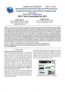
Superscalar CPU design emphasizes improving the instruction dispatcher accuracy, and allowing it to keep the multiple functional units in use at all times. This has become increasingly important when the number of units increased. While early superscalar CPUs would have two ALUs and a single FPU, a modern design such as the PowerPC 970 includes four ALUs, two FPUs, and two SIMD units. If the dispatcher is ineffective at keeping all of these units fed with instructions, the performance of the system will suffer. A superscalar processor usually sustains an execution rate in excess of one instruction per machine cycle. But merely processing multiple instructions concurrently does not make an architecture superscalar, since pipelined, multiprocessor or multi-core architectures also achieve that, but with different methods. In a superscalar CPU the dispatcher reads instructions from memory and decides which ones can be run in parallel, dispatching them to redundant functional units contained inside a single CPU. Therefore a superscalar processor can be envisioned having multiple parallel pipelines, each of which is processing instructions simultaneously from a single instruction thread[7],[8],[9]. The block diagram of the existing RISC processor is shown in the diagram along with its instruction cycle
(a)
(b) The simple superscalar pipeline is shown in the figure Figure2: Block diagram of RISC processor with single instruction and single execution IN above block diagram only P0 acts as address and data ports. Coming to data size, only 16 bit ports are available.
Figure1: Simple superscalar pipeline
Single instruction single execution scheme is performed in instruction execution life cycle. Either asynchronous or synchronous only, two modes are available with above processor.
International Journal of VLSI & Signal Processing Applications, Vol. 2,Issue2,April 2012, ISSN 2231-3133, (153-159)
Available performance improvement from superscalar techniques is limited by three key areas:
The degree of intrinsic parallelism in the instruction stream, i.e. limited amount of instruction-level parallelism. The complexity and time cost of the dispatcher and associated dependency checking logic. The branch instruction processing.
Existing binary executable programs have varying degrees of intrinsic parallelism. In some cases instructions are not dependent on each other and can be executed simultaneously. In other cases they are inter-dependent: one instruction impacts either resources or results of the other. The instructions a = b + c; d = e + f can be run in parallel because none of the results depend on other calculations. However, the instructions a = b + c; b = e + f might not be runnable in parallel, depending on the order in which the instructions complete while they move through the units. When the number of simultaneously issued instructions increases, the cost of dependency checking increases extremely rapidly. This is exacerbated by the need to check dependencies at run time and at the CPU's clock rate. This cost includes additional logic gates required to implement the checks, and time delays through those gates. Research shows the gate cost in some cases may be nk gates, and the delay cost k2log n, where n is the number of instructions in the processor's instruction set, and k is the number of simultaneously dispatched instructions. In mathematics, this is called a combinatoric problem involving permutations. Even though the instruction stream may contain no interinstruction dependencies, a superscalar CPU must nonetheless check for that possibility, since there is no assurance otherwise and failure to detect a dependency would produce incorrect results. No matter how advanced the semiconductor process or how fast the switching speed, this places a practical limit on how many instructions can be simultaneously dispatched. While process advances will allow ever greater numbers of functional units (e.g., ALUs), the burden of checking instruction dependencies grows so rapidly that the achievable superscalar dispatch limit is fairly small. -- likely on the order of five to six simultaneously dispatched instructions. However even given infinitely fast dependency checking logic on an otherwise conventional superscalar CPU, if the instruction stream itself has many dependencies, this would also limit the possible speedup. Thus the degree of intrinsic parallelism in the code stream forms a second limitation. Collectively, these limits drive investigation into alternative architectural changes such as Very Long Instruction Word (VLIW), Explicitly Parallel Instruction Computing (EPIC), simultaneous multithreading (SMT),
and processors. With VLIW, the burdensome task of dependency checking by hardware logic at run time is removed and delegated to the compiler. Explicitly Parallel Instruction Computing (EPIC) is like VLIW, with extra cache prefetching instructions. Simultaneous multithreading, often abbreviated as SMT, is a technique for improving the overall efficiency of superscalar CPUs. SMT permits multiple independent threads of execution to better utilize the resources provided by modern processor architectures. Superscalar processors differ from multi-core processors in that the redundant functional units are not entire processors. A single processor is composed of finer-grained functional units such as the ALU, integer multiplier, integer shifter, floating point unit, etc. There may be multiple versions of each functional unit to enable execution of many instructions in parallel. This differs from a multi-core processor that concurrently processes instructions from multiple threads, one thread per core. It also differs from a pipelined CPU, where the multiple instructions can concurrently be in various stages of execution, assemblyline fashion. The various alternative techniques are not mutually exclusive—they can be (and frequently are) combined in a single processor. Thus a multicore CPU is possible where each core is an independent processor containing multiple parallel pipelines, each pipeline being superscalar. Some processors also include vector capability.
III PROPOSED RISC PROCESSOR USING VLIW Now coming to our paper the main implementation of the RISC processor is done by using VLIW architecture along with S.I.M.E (Single Instruction and Multiple Execution) instruction cycle Very long instruction word or VLIW refers to a CPU architecture designed to take advantage of instruction level parallelism (ILP). A processor that executes every instruction one after the other (i.e. a non-pipelined scalar architecture) may use processor resources inefficiently, potentially leading to poor performance. The performance can be improved by executing different sub-steps of sequential instructions simultaneously (this is pipelining), or even executing multiple instructions entirely simultaneously as in superscalar architectures. Further improvement can be achieved by executing instructions in an order different from the order they appear in the program; this is called out-of-order execution. The VLIW approach, on the other hand, executes operations in parallel based on a fixed schedule determined when programs are compiled. Since determining the order of execution of operations (including which operations can execute simultaneously) is handled by the compiler, the
International Journal of VLSI & Signal Processing Applications, Vol. 2,Issue2,April 2012, ISSN 2231-3133, (153-159)
processor does not need the scheduling hardware that the three techniques described above require. As a result, VLIW CPUs offer significant computational power with less hardware complexity (but greater compiler complexity) than is associated with most superscalar CPUs [10].
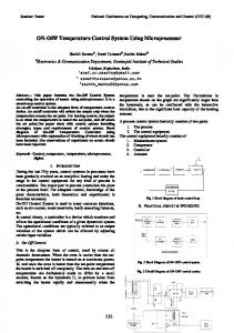
lacks its power consumption, possible design defects and other negative features. In a VLIW, the compiler uses heuristics or profile information to guess the direction of a branch. This allows it to move and prescheduled operations speculatively before the branch is taken, favouring the most likely path it expects through the branch. If the branch goes the unexpected way, the compiler has already generated compensatory code to discard speculative results to preserve program semantics. The main block diagram of our pipelined risc processor using VLIW architecture along with single instruction and multiple execution instruction life cycle is shown in figure
In contrast, one VLIW instruction encodes multiple operations; specifically, one instruction encodes at least one operation for each execution unit of the device. For example, if a VLIW device has five execution units, then a VLIW instruction for that device would have five operation fields, each field specifying what operation should be done on that corresponding execution unit. To accommodate these operation fields, VLIW instructions are usually at least 64 bits wide, and on some architectures are much wider. For example, the following is an instruction for the SHARC. In one cycle, it does a floatingpoint multiply, a floating-point add, and two auto increment loads. All of this fits into a single 48-bit instruction.
(a)
f12=f0*f4, f8=f8+f12, f0=dm(i0,m3), f4=pm(i8,m9); Since the earliest days of computer architecture some CPUs have added several additional arithmetic logic units (ALUs) to run in parallel. Superscalar CPUs use hardware to decide which operations can run in parallel. VLIW CPUs use software (the compiler) to decide which operations can run in parallel. Because the complexity of instruction scheduling is pushed off onto the compiler, the hardware's complexity can be substantially reduced. A similar problem occurs when the result of a parallelizable instruction is used as input for a branch. Most modern CPUs "guess" which branch will be taken even before the calculation is complete, so that they can load up the instructions for the branch, or (in some architectures) even start to compute them speculatively. If the CPU guesses wrong, all of these instructions and their context need to be "flushed" and the correct ones loaded, which is time-consuming. This has led to increasingly complex instruction-dispatch logic that attempts to guess correctly, and the simplicity of the original RISC designs has been eroded. VLIW lacks this logic, and therefore
(b) Figure3: pipelined RISC processor using VLIW and S.I.M.E instruction cycle The description for the main blocks of 32-bit pipelined RISC processor is explained as below In above block diagram; Both P0 and P1 can be acts as address as well as data ports. All ports are 32 bit, simultaneously they can be accessible In instruction life cycle, one new methodology is implemented called GALS (Global asynchronous Local Synchronous). With this concept, time is reduced and power consumption is also decreases. Along with that S.I.M.E scheme is also implemented to achieve high throughput
International Journal of VLSI & Signal Processing Applications, Vol. 2,Issue2,April 2012, ISSN 2231-3133, (153-159)
A. program counter
C.Instruction cycle
It performs the two operations, namely, incrementing and loading. Depending on the details of the particular computer, the PC or IP holds either the memory address of the instruction being executed, or the address of the next instruction to be executed. the program counter is incremented automatically after fetching a program instruction, so that instructions are normally retrieved sequentially from memory, with certain instructions, such as branches, jumps and subroutine calls and returns, interrupting the sequence by placing a new value in the program counter[11].
This instruction cycle is having five main parts. They are
The Program Counter (PC) is just one of the many registers in the hardware of the CPU. It, like each of the other registers, consists of a bank of binary latches (a binary latch is also known as a flip-flop), with one flip-flop per bit in the integer that is to be stored (32 for a 32-bit CPU, for example). In the case of the PC, the integer represents the address in memory that is to be fetched next. B. Arithmetic and Logic unit
Instruction fetch (IF) – get instruction from memory, increment pc Instruction decode (ID) – translate opcode into control signals and read registers Output fetch (OF) – fetches out the output Execute (EXE) – perform ALU operations, compute jump/branch targets Write back(WB) – update register file
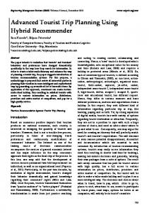
IV. SIMULATION RESULTS The RISC processor described above is designed using VHDL and is simulated. The simulation results show that the processor is capable of implementing the given instructions and gives multiple executions, thereby satisfying the basic requirements of the RISC processor. In the results at first we are showing the p0 address and p2data mode results
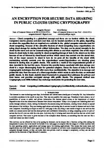
The arithmetic and logic unit (ALU) performs arithmetic and logic operations. It also performs the bit operations such as rotate and shift by a defined number of bit positions. Here in this architecture the ALU is doing multiple operations at a time. In computing, an arithmetic logic unit (ALU) is a digital circuit that performs arithmetic and logical operations. The ALU is a fundamental building block of the central processing unit of a computer, and even the simplest microprocessors contain one for purposes such as maintaining timers. The processors found inside modern CPUs and graphics processing units (GPUs) accommodate very powerful and very complex ALUs; a single component may contain a number of ALUs[12]. In our proposed architecture ALU executes multiple operations because of VLIW architecture. A simple example is shown in the figure
Figure 5: P0 address mode
Figure4: A simple example arithmetic logic unit (2-bit ALU) that does AND, OR, XOR, and addition. Figure 6: p2 data mode
International Journal of VLSI & Signal Processing Applications, Vol. 2,Issue2,April 2012, ISSN 2231-3133, (153-159)
V. CONCLUSION The design of a 32-Bit pipelined RISC processor using VLIW architecture has implemented. Along with that S.I.M.E scheme is also implemented to achieve high throughput than by using super scalar architecture. Here we are having multiple executions with single instructions because of VLIW architecture. Furthermore this design can be applicable to various general and DSP applications. REFERENCES [1]
Figure7: simulation results showing Swapping
Figure8: simulation results showing increment
As we mentioned p0 and p1 acts asa both data and address modes we had showed the results of address mode of p0 and data mode of p2 in fig5 and 6 As the processor has the different instructions we showed swapping and increment of bits in the results
Here Fig 7 shows the simulation results of swapping of bits .Mainly this operation is done in ALU.The main operations of the risc processor are done in ALU Here Fig 8 shows the simulation results of increment. It is one of the main operation of ALU.There are so many operations can be done in ALU but here we mainly concentrated on swapping and increment.
Reduced instruction set computer." Whatis?com: 9 Aug 2000, http://whatis.techtarget.com/WhatIs_Definition_Page/0,415 2,214266,00.html [2] The Future of Formal Methodsand GALS Design by Kenneth S. Stevens Daniel Gebhardt Junbok You Yang XuVikas Vij Shomit Das Krishnaji Desai in Electrical and Computer Engineering atUniversity of Utah,Salt Lake City, U.S.A [3] "Introduction to RISC." http://www.inf.fhdortmund.de/person/prof/si/risc/intro_to_risc/irt0_index.ht ml [4] Introduction to risc processor by ni logic pvt.ltd.,pune [5] The Pipelined RiSC-16 ENEE 446: Digital Computer Design, Fall 2000 by Prof. Bruce Jacob [6] Wayne, Peter. "Processor Pipelines." Byte, 17 (1992): 305 [7] Zhou & Martonosi. ―Augmenting Modern Suuperscalar Architectures with ConfigurableExtended Instructions‖.19 April 2004. [8] Sorin Cotofana, Stamatis Vassiliadis, "On the Design Complexity of the Issue Logic of Superscalar Machines", EUROMICRO 1998: 10277-10284 [9] Steven McGeady, "The i960CA SuperScalar Implementation of the 80960 Architecture", IEEE 1990, pp. 232–240 [10] Fisher, Joseph A. (1983). "Very Long Instruction Word architectures and the ELI-512" (PDF). Proceedings of the 10th annual international symposium on Computer architecture. International Symposium on Computer Architecture. New York, NY, USA: ACM pp. 140–150. doi:10.1145/800046.801649. ISBN 0-89791-101-6 Retrieved 2009-04-27. [11] F.B. Chambers, D.A. Duce and G.P. Jones (1984), Distributed Computing, Academic Press, Orlando, USA, ISBN 0-12-167350-2. [12] Hwang, Enoch (2006). Digital Logic and Microprocessor Design with VHDL. Thomson. ISBN 0-534-46593-5.
International Journal of VLSI & Signal Processing Applications, Vol. 2,Issue2,April 2012, ISSN 2231-3133, (153-159)