Company Limited, NEC Electronics Corporation, Renesas. Technology Corporation, Toshiba Corporation, Cadence De- sign Systems Inc and Synopsys Inc.
Int'l Conf. Reconfigurable Systems and Algorithms | ERSA'08 |
201
Implementation of a Multi-Context FPGA Based on Flexible-Context-Partitioning Waidyasooriya Hasitha Muthumala, Masanori Hariyama and Michitaka Kameyama Graduate School of Information Sciences, Tohoku University Aoba 6-6-05, Aramaki, Aoba, Sendai, Miyagi,980-8579, Japan Email: {hasitha@kameyama., hariyama@, kameyama@}ecei.tohoku.ac.jp Abstract— This paper presents a novel architecture to increase the hardware utilization in multi-context field programmable gate arrays (MC-FPGAs). Conventional MC-FPGAs use dedicated tracks to transfer context-ID bits. As a result, hardware utilization ratio decreases, since it is very difficult to map different contexts area efficiently. It also increases the context switching power, area and static power of the context-ID tracks. Proposed MC-FPGA uses same wires to transfer both data and context-ID bits from cell to cell. As a result, programs can be mapped area efficiently by partitioning them into different contexts. We also propose an asynchronous multi-context logic block architecture to increase the processing speed of the multiple contexts. The proposed architecture is designed using 6-metal 1poly CMOS design rules. The data and context-ID transfer delays are measured to be 2.03ns and 2.26ns respectively. Keywords— DPGA, multi-context, asynchronous FPGA.
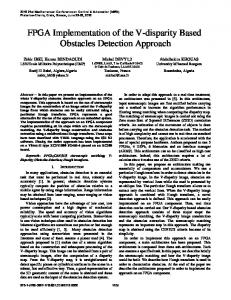
Fig. 1.
Multi-context LUT
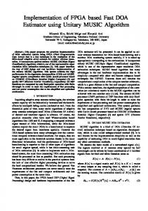
I. I NTRODUCTION Dynamically programmable gate arrays (DPGAs) are introduced to increase the logic and interconnect utilization [1] in conventional FPGAs. Even the descriptive size of a program is larger than the physical resources available, it can be implemented in a DPGA by breaking into different subprograms that execute in independent time slots and share the same resources. The most popular DPGA architecture is the multi-context FPGA (MC-FPGA) [2]. In MC-FPGAs, each program or application are assigned to a separate context. The configuration data belongs to each context are stored in different configuration planes. To execute a particular program, the appropriate context-ID is passed to the logic and interconnect elements. According to the context-ID, configuration data in the relevant configuration plane are selected. Fig.1 shows a multi-context LUT, which is the main component of a multicontext logic block. It has separate sets of configuration bits for each context. The multiplexers at the top in Fig.1 select the appropriate set of configuration bits according to the contextID. Then the multiplexer at the bottom selects the relevant configuration bit according to the input data, similar to a single context FPGA. Figure 2 shows the context-ID distribution in typical MCFPGA. All the logic blocks and multi-context switches share the same context-ID signal. As a result. when the context-ID changes, the whole chip changes into a different context. In order to make this change faster, the context-ID tracks are designed quite similar to the typical clock tree. Moreover, in
Fig. 2.
Context-ID distribution in typical MC-FPGA
a 4-context FPGA, two dedicated context-ID tracks are needed to distribute the 2 context-ID bits. Similarly, when the number of context-ID bits doubles, an extra context-ID track is needed. These tracks occupy a large area and consume a large power in both static and dynamic states. According to [3], [4] and [5], more than 20% of the power consumption in FPGAs is due to the clock distribution and 60% is due to the interconnection network. In addition to that, dynamic power is consumed due the context switching and static power is consumed due to the context-ID distribution network in MC-FPGAs. If we assume the structure of the context-ID track is quite similar to a clock-tree, we can save a considerable share of power by removing context-ID tracks. The typical context-ID distribution reduces the flexibility of context mapping and decreases the hardware utilization. In this research, we focus on the large power consumption and low hardware utilization in typical MC-FPGAs. We propose a localized context-ID distribution to increase the hardware utilization. Since the proposed architecture does not
202
Int'l Conf. Reconfigurable Systems and Algorithms | ERSA'08 |
(a) Partitioned DFG Fig. 4. (a) Scheduled DFGs Fig. 3.
(b) configuration memory usage
Ex.2: Overlapped configuration memory
(b) Configuration memory usage
Ex.1: Wasted configuration memory
contain dedicated context-ID tracks, the power consumption and area due to the context-ID distribution is reduced. The proposed interconnection network requires less area and consumes less power than the typical one. II. F LEXIBLE CONTEXT PARTITIONING In typical MC-FPGAs, contexts are executed sequentially so that the same resources are reused in different time slots. However smaller contexts increase the logic and interconnect area and redundant contexts increase configuration memory as explained in Sec.II-A. Therefore, our idea is to run contexts both sequentially and parallelly, so that smaller but mutually independent contexts run together parallelly while the dependent ones run sequentially. Flexible context partitioning refers to dividing the hardware resources into different partitions and assigning different parts of the applications area effectively. Partitions can be resized, deleted and recreated in reconfiguration. A. Problems related to the global context-IDs We explain the problems in hardware utilization using following examples. Let us consider two mutually independent programs assigned to two contexts as shown in Fig.3(a). We assume that the configuration memory needed by both DFGs are very small compared to the memory available in a single configuration plane. If we map the two contexts onto two configuration planes as shown in Fig.3(b), we get a large wasted configuration memory area. This problem can be solved by assigning both DFGs to a single context or map two contexts onto a single configuration plane. However, assigning both DFGs to a single context is impossible since the execution time of the programs are unknown. Mapping two contexts onto a single configuration plane is also impossible, since the context-ID of the whole chip changes simultaneously, so that a single configuration plane can hold the configuration of a single context. Figure 4(a) shows a large DFG partitioned to two contexts. However, part of the DFG is same in both, context 1 and context 2. As a result, same configuration data are included in two configuration planes after mapping, as shown in Fig.4(b). Therefore, part of the configuration area is wasted for these redundant data.
Fig. 5.
Local context-ID distribution
B. Context-Partitioning using Locally distributed context-IDs In order to solve the above problems, we propose a locally distributed context-ID distribution that allows flexible-contextpartitioning. As shown in Fig.5, context-ID transfers from cell-to-cell and it is distributed only in a part of the chip that required by a particular context. Therefore, we call it a local context-ID. There can be more than one local contextID in the same chip at different areas simultaneously. The context-ID signal is guided to the next cell by a context-ID decoder (CID). The detailed architecture of a CID is explained in Sec.III. In the proposed architecture, all the applications are partitioned into sub-contexts. A sub-context is a program or a sub-program. More than one sub-context can be mapped to a single configuration plane unlike a context. A sub-context is accessed by a local context-ID. There can be more than one sub-contexts mapped into a single configuration plane. In Fig.6, two DFGs are assigned to two sub-contexts. Then those two sub-contexts are mapped onto a single configuration plane. Since we are using local context-IDs, it is possible to map two contexts with different execution timings onto a single configuration plane. The remaining configuration planes can be used to store another sub-context. In Fig.7, similar circuits are assigned to a single sub-context. The other two parts are assigned to different sub-contexts. As a result, we do not get the same configuration data stored
Int'l Conf. Reconfigurable Systems and Algorithms | ERSA'08 |
(a) Partitioned DFG
203
(b) configuration memory usage Fig. 6.
Solution for Ex.1
(a) Switch element (SE) Fig. 8.
(a) Partitioned DFG Fig. 7.
(b) configuration memory usage Solution for Ex. 2
III. OVERALL ARCHITECTURE A. Decoder based interconnection network We adopt the interconnection block architecture proposed in the paper [8] since it efficiently reduces the area by 50%. The main idea behind this architecture is the redundancy in the configuration data. Since more than 90% of the configuration
Switch block structure
(a) Context-ID independent configuration Fig. 9.
in different configuration planes. The sub-contexts 1 and 2 are executed until the time is t1 and sub-contexts 1 and 3 are executed next. Note that, the logic and wire area corresponding to the of sub-context 3 must not be overlapped with the area corresponding to the sub-context 1, because in this case, different configuration planes are accessed simultaneously. Some of the existing MC-FPGA architectures are capable of doing flexible context partitioning. PACT Xpp [6] uses a runtime and partial reconfiguration mechanism, so that only the required resources have to be changed in each reconfiguration. However, the reconfiguration mechanism is very complex and needs dedicated configuration buses. Therefore the overhead for the reconfiguration is very large. This increases the area as well as the power consumption. PCA [7] provides a dynamically reconfigurable asynchronous architecture. It consists with two hardware planes, One is to implement the computations and the other is to implement data path and reconfiguration mechanism. However, this mechanism is based on re-writing SRAMs so that it is very slow and takes about 60µs for each reconfiguration. As a result, it cannot be used in applications that requires fast context switching.
(b) Switch block (SB)
(b) Context-ID configuration
dependent
Implementation of the configuration-bit-patterns
data are redundant [9], they can be implemented by a simple switch structure smaller than the conventional multi-context switch (MC-Switch). This simplified switch is called “switch element (SE)” and shown in Fig.8(a). Figure 9(a) shows the implementation of an MC-Switch when the configuration data are independent of the context-ID (always diconnected). Figure 9(b) shows the implementation when the configuration data depend on a single context-ID bit (C1). However, when a configuration depends on more than a single context-ID bit, it cannot be implemented using a single SE. In this case, the context-ID bits are decoded into a different control signal and then pass it to the variable input of an SE. To create decoders, a structure called “switch block (SB)” is used. An SB consists with two SEs aligned vertically and horizontally as shown in Fig.8(b), so that it can act as a pass gate or a crossbar switch. It is the basic unit of the interconnection architecture. Figure 10 shows an example where the configuration bit depends on both context-IDs, C0 and C1. According to Fig.10(a), LB1 and LB2 are connected only when both context-ID bits are 1. Therefore, a set of SEs are connected to generate the control signal [U = C0 · C1] using the context-IDs C0 and C1. Then this control signal is passed to the variable input of an SE. All the other SEs in the path between LB1 and LB2 are programmed as always connected. As a result, the connection patterns shown in Fig.10(a) can be implemented. A detailed description on routing and creating decoders is given in [8].
204
Int'l Conf. Reconfigurable Systems and Algorithms | ERSA'08 |
(a) Configuration table
Fig. 11.
(b) Implementation Fig. 10.
Configurations depend on a several context-IDs
Fig.11 shows the overall architecture of the interconnection network that use to transfer local context-ID and data. In this architecture, local context-ID is passed to the MC-FPGA through the I/O ports. Then it is stored in the LBs connected to those I/O ports. The stored context-ID bits are connected to decoders, so that the decoders can decide the next data paths. After the data path is decided, the local context-ID travels through that path to another LB. Similarly the local contextID bits are stored again and then passed to decoders. When this process continuous, all the logic blocks needed by a particular sub-context receive the local context-ID bits. At the same time, the data paths among the LBs are automatically created. Once the data paths are created, data are sent through those paths. All the data paths in all the sub-contexts are decided in the high-level-synthesis, and decoders are programmed using those information. The proposed interconnect architecture can map several sub-contexts to a single configuration plane. However, each sub-context has different critical path delays. Therefore, their processing speeds vary. Since each configuration plane is corresponding to the same logic and interconnect area, it is impossible to use different clock frequencies for different sub-contexts simultaneously, unless there are several clock distribution networks. It is very difficult to use different clock distributions, since the power consumption due to the clock tree is quite high according to [4] and [5]. When several sub-contexts are executed at the same time, the worst case
Overall architecture
delay is used to determine the clock frequency for all the subcontexts. As a result, faster sub-contexts also run in a slower speed. However, using an asynchronous architecture, different sub-contexts can run in different speeds. Single context asynchronous FPGAs are proposed in many papers such as [10] and [11] but no proposals for MC-FPGAs which we think the asynchronous architecture is most suitable. According to [12], asynchronous architectures increase the performance by nearly 30% compared to synchronous ones. Since the same tracks are used to transfer both data and context-IDs, we need another signal to separate context-ID bits from data bits. For this purpose, a new signal denoted by C is used. In this paper, the term “CVR encoding” is used for this encoding scheme, since it requires three signals C, V and R to transfer a data bit or a context-ID bit. The encoded signals and their decoded values are shown in Fig.12. The phase equals to [C ⊕ V ⊕ R] and the data bit equals to V . If the phase is changed, it indicates a new signal is received. If C is “0”, the current bit is a data bit, and otherwise it is a context-ID bit. An example of a bit-serial data and context-ID transfer is shown in Fig.13. At the beginning, three data bits [0 0 1] are received in a bit-serial manner. Then C changes from “0” to “1” indicating the next bit is a context-ID-bit. After that, the context-ID-bits are received one after another. In this example, the received context-ID equals to 3 (011). After all three context-ID-bits are received, C changes from “1” to “0” indicating the next bit is a data bit. B. Architecture of the logic block The block diagram of a logic block (LB) in the proposed MC-FPGA is shown in Fig.14. The proposed LB has 3 main components. 1) Receiver 2) Transmitter 3) Multi-context look-up-table (LUT) The receiver circuit receives C, V, R values from previous LBs. When both input C values are “0”, the receiver passes V, R values to the LUT. When the C values change from “0” to “1”, the context-ID bits are stored in the shift register in the
Int'l Conf. Reconfigurable Systems and Algorithms | ERSA'08 |
205
Fig. 14. Fig. 12.
Fig. 13.
Block diagram of a logic block
CVR encoding
Data transfer based on CVR encoding
receiver. After a context-ID bit is saved in the shift register, the receiver sends the acknowledge (ACK) signals to the previous LBs, indicating it is ready to receive another bit. After all the context-ID bits are received, the transmitter starts sending the appropriate V, R values of the context-ID bits to the next LBs. The multiplexers select the LUT output when C is “0” and the transmitter output when C is “1”. The control signal of the multiplexer is delayed for one cycle, so that it can select data and context-ID accurately as shown in Fig.13. The architecture of a 2-input-8-context LUT is shown in Fig.15. It has 4 memory bits per each context to function as a programmable 2-input logic gate. When the appropriate configuration plane is selected according to the context-IDbits, the relevant memory bits are passed to the decoders. The structure of the decoder-11 in Fig.15 is shown in Fig.16. When the phase of the both inputs ( [Va,Ra] and [Vb,Rb] ) are “0”, both V and R are equal to the memory bit M11, so that the output phase equals to the input phase after the calculation. Similarly, when the phase is “1”, V equals to M11 and R equals to M 11. Note that, when the phases are different, both V and R become high-impedance, so that the values in the latches are preserved. Also note that, in every case, both inputs have the same C value. If C is different, the inputs to the LUT will be blocked by the receiver, so that the previous state of the latch is preserved. This multi-context LUT is a modification of the single context LUT proposed in [11].
Fig. 15.
Architecture of the multi-context LUT
IV. E VALUATION Performance of the proposed MC-FPGA is compared with the typical synchronous MC-FPGA, under 90nm CMOS technology using HSPICE circuit simulation. For the comparison, following assumptions are considered. The area of logic blocks is 30% of the total area of a typical MC-FPGA and the rest of the area is occupied by the switch blocks. Using this assumption, we calculated the ratio between the number of logic blocks and the switch blocks. The same ratio is applied to the proposed MC-FPGA. The frequency of the typical MC-FPGA and the data-rate of the proposed one are set to 100MHz. The area, power and peak current due to clock tree and context-ID tracks are not considered for this evaluation. Table I shows the comparisons of the proposed architecture with the typical MC-switch based interconnect architecture. The proposed switch block is smaller than the typical 8-context switch so that the interconnect area is smaller than that of the typical architecture. Static power is also small since the number of transistors in the proposed SB is smaller compared to a typical MC-switch. However, the area of an LB is 3 times larger than that of a typical multi-context LB. The static power is also large for LBs. Since, LEDR data transfer is used, two wires are needed to transfer a single bit. As a result, area
206
Int'l Conf. Reconfigurable Systems and Algorithms | ERSA'08 | TABLE I P ROPOSED MC-FPGA V S . T YPICAL MC-FPGA ( NUMBER OF CONTEXT = 8)
Normalized area Normalized peak current Normalized context switching power Normalized static power
Fig. 16.
Interconnects Typical Proposed 1 0.78
Logic Blocks Typical Proposed 1 2.9
Typical 1
Total Proposed 1.39
1
0.49
1
0.81
1
0.57
1
0.43
1
0.72
1
0.68
1
0.84
1
6.1
1
4.17
Structure of the decoder-11
is approximately 2 times larger than that of a synchronous LB. We also use muller C elements to detect the changes in data. Shift registers are also included in LBs to store contextID bits. In MC-FPGAs, most of the area is occupied by the switch blocks, so that we can hide the disadvantages of the LBs among the advantages of switch blocks. Moreover, we have not considered the power consumption and area due to the clock tree and context-ID tracks in typical MC-FPGAs. According to [3], [4] and [5], more than 20% of the power consumption in FPGAs is due to clock network. Therefore, if we consider those factors into the evaluation, proposed architecture provides much better results. The peak current and the context switching power are calculated by assuming only the 50% of the circuit is switched. When only half of the circuit is reconfigured in the proposed MC-FPGA, peak current and context switching power is low. In the typical MC-FPGA, the whole chip has to be reconfigured when the contexts are switched, so that the context switching power is high. Figure 17 shows the chip micrograph of the designed test chip under 90nm 6-metal 1-poly CMOS design rules. The designed chip has a 10 × 10 cell array. Figure 18 shows the measured delay for 99 cells connected in series. Table II shows the other measured performance of the chip. V. C ONCLUSION We have proposed a novel MC-FPGA architecture that uses the configuration memory very effectively by dividing the applications into sub-contexts. The execution timings of different sub-contexts can be overlapped, unlike the contexts in the typical MC-FPGAs. Sub-contexts are controlled by a
Fig. 17.
Fig. 18.
Chip micrograph
Data transfer delay for series connection of 100 cells
local context-ID signal that is transferred from cell-to-cell, using the same data tracks. As a result, the area overhead and power consumption due to dedicated context-ID tracks are reduced. According to the experimental results shown in Table I, the context switching power is only 68% of the typical MCFPGA architecture when 50% of the contexts are switched. The peak current when the context are switched is also reduced to 57%. Since only a part of the circuit is affected when the context are switched, both context switching power an peak current are reduced. Peak current and context switching power is reduced further if less than 50% of the circuit is switched simultaneously. The proposed local context-ID signal can be produced internally from LBs, so that we can perform area
Int'l Conf. Reconfigurable Systems and Algorithms | ERSA'08 | TABLE II P ERFORMANCE OF THE PROPOSED MC-FPGA Number of contexts Number of cells Cell area Minimum context ID transfer delay (for 3 context-ID bits) Minimum data transfer delay for one cell
8 100 (10 × 10) 53 × 62 (µm2 ) 2.26 ns 2.03 ns
and power effective implementation of conditional branches. However, to gain maximum performance from the proposed architecture, we need a very powerful CAD tool. The proposed architecture can execute more than one sub-context simultaneously even they are not belongs to the same configuration plane. As a result, conflicts can occur, if two sub-contexts, belong to two different context planes, are corresponding to the same logic and wire area at the same time. These conflicts can be solved in high level synthesis by careful analysis of sub-context timing and dependencies. Therefore, the CAD tool must be able to do the global sub-context scheduling as well as the all the other tasks, such as logic optimization, allocation, etc. ACKNOWLEDGMENT This work is supported by VLSI Design and Education Center (VDEC), the University of Tokyo in collaboration with STARC, Fujitsu Limited, Matsushita Electric Industrial Company Limited, NEC Electronics Corporation, Renesas Technology Corporation, Toshiba Corporation, Cadence Design Systems Inc and Synopsys Inc. R EFERENCES [1] A. DeHon, “Dynamically programmable gate arrays: A step toward increased computational density”, Proc. the Fourt Canadian Workshop on Field-Programmable Devices, pp.47-54, 1996. [2] S. Trimberger, “A time-multiplexed FPGA”, 5th IEEE Symposium on FPGA-Based Custom Computing Machines, pp.22-28, 1997. [3] E. Kusse and J. Rabaey, “Low-Energy Embedded FPGA Structures” ISLPED, pp.155-160, 1998. [4] L. Shang, A. S. Kaviani and K. Bathala, Dynamic Power Consumption in VirtexT M -II FPGA Family, FPGA’02, pp.157-164, February 2002. [5] F. Li, Y. Lin, L. He, D. Chen and J. Cong, “Power Modeling and Characteristics of Field Programmable Gate Arrays”, IEEE Trans. on Computer-Aided Design of Integrated Circuits and Systems, Vol. 24, No.11, pp.1712-1724, November 2005. [6] V. Baumgarte, G. Ehlers, F. May, A, Nuckel A, M. Vorbach and M. Weinhardt, “PACT XPP-A Self-Reconfigurable Data Processing Architecture”, A The Journal of Supercomputing, Vol.26, No.26, pp.167184, 2003. [7] R. Konishi, H. Ito, H. Nakada, A. Nagoya, K. Oguri, N. Imlig, T. Shiozawa, M. Inamori and K. Nagami, “PCA-1: a fully asynchronous, self-reconfigurable LSI”, Asynchronous Circuits and Systems (ASYNC), pp.54-61, 2001. [8] W. Chong, M. Hariyama and M. Kameyama, “Novel switch-block architecture using reconfigurable context memory for multi-context FPGAs”, Proc. International Workshop on Applied Reconfigurable Computing (ARC 2005), pp.99-102, 2005. [9] I. Kennedy, “Exploiting redundancy to speedup reconfiguration of an FPGA”, Proc. 13th International Conference on Field Programmable Logic and Application, pp.262-271, September 2003. [10] C. Traver, R.B Reese and M.A. Thornton, “Cell designs for self-timed FPGAs”, Proc. 14th Annual IEEE International ASIC/SOC Conference, pp.175-179, 2001.
207
[11] M. Hariyama, S. Ishihara, C. C. Wei and M. Kameyama, “A FieldProgrammable VLSI Based on an Asynchronous Bit-Serial Architecture”, IEEE Asian Solid-State Circuits Conference (A-SSCC), pp.380383, November 2007. [12] Y. Adachi, K. Ishikawa, S. Tsutsumi and H. Amano, “An implementation of the Rijndael on Async-WASMII” IEEE International Conference on Field-Programmable Technology (FPT), pp.44-51, 2003.