1128
IEEE ELECTRON DEVICE LETTERS, VOL. 31, NO. 10, OCTOBER 2010
Low-Frequency Noise Performance of a Bilayer InZnO–InGaZnO Thin-Film Transistor for Analog Device Applications Sanghun Jeon, Sun Il Kim, Sungho Park, Ihun Song, Jaechul Park, Sangwook Kim, and Changjung Kim
Abstract—In this letter, we present a comparative study of the low-frequency noise behavior of single-layer InGaZnO and bilayer InZnO–InGaZnO thin-film transistors (TFTs). The normalized noise for the bilayer oxide TFT is three times lower than that for the single-layer oxide TFT, mainly due to the higher mobility of the thin interfacial InZnO layer. The carrier number fluctuation is the dominant low-frequency noise mechanism in both devices. The use of a high-mobility bilayer oxide TFT with scaled gate length is still valid for reducing low-frequency noise. Index Terms—Analog device applications, bilayer oxide semiconductor, electron devices, noise performance, thin-film devices, thin-film transistor (TFT).
S
INCE the report of Nomura et al. [1], many studies have been focusing on developing and optimizing electronically active oxide thin-film transistors (TFTs) using amorphousIn–Ga-Zn-O (a-IGZO) semiconductor. Amorphous-IGZO TFTs have excellent features such as high saturation mobilities (∼10 cm2 /eV/s), low Ioff leakage current, gentle subthreshold slope, negligible Vth distribution throughout the wafer owing to the amorphous structure [2]–[4]. In particular, a-IGZO TFTs having optical transparency, low-temperature process capability, and excellent process compatibility with the existing technology for mass production of a-Si:H TFTs have received considerable attention for a wide range of device applications, including liquid crystal displays [5], organic light-emitting diodes [6], see-through devices [7], and flexible electronics [8]. Many device properties of amorphous oxide TFTs are critically dependent on the characteristics of the semiconductor-gate insulator interface and the amorphous active semiconductor having a significant number of subgap states [9], [10]. Among the various properties of amorphous oxide TFTs, low-frequency noise is an important issue to be considered for analog device applications. Alternatively, noise investigations have the potential to be used as a reliability tool, as low-frequency noise is a parameter that is highly sensitive to technology [11], [12]. There have been a few studies on Manuscript received June 7, 2010; revised June 28, 2010; accepted July 8, 2010. Date of publication September 2, 2010; date of current version September 24, 2010. The review of this letter was arranged by Editor A. Nathan. S. Jeon, S. I. Kim, I. Song, J. Park, S. Kim, and C. Kim are with the Semiconductor Device Laboratory, Samsung Advanced Institute of Technology, Samsung Electronics Corporation, Gyeonggi 449-712, Korea. S. Park is with the Department of Chemistry, Daejin University, Gyeonggi-do 487-711, Korea (e-mail:
[email protected]). Color versions of one or more of the figures in this letter are available online at http://ieeexplore.ieee.org. Digital Object Identifier 10.1109/LED.2010.2059694
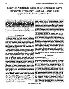
the low-frequency noise behaviors of a-IGZO TFTs [13]. The gate dielectric materials used in previous low-frequency noise studies on a-IGZO TFTs are Al2 O3 with a strong trapping characteristic, and thus, there is high noise level for a-IGZO TFTs [13]. Currently, greater understanding of the low-frequency noise of amorphous oxide TFTs in various aspects is required for the development of oxide TFTs for the aforementioned applications. In our study, SiO2 was used as a gate dielectric to lower the low-frequency noise of an a-IGZO TFT. We present the influence of mobility on the low-frequency noise performance of an amorphous oxide TFT by comparing single-layer IGZO (μsat of 10 cm2 /eV/sec) and bilayer IZO–IGZO (μsat of 30 cm2 /eV/sec) TFTs, with the latter providing low-noise performance. In addition, it is found that the fluctuation of the carrier number is the dominant low-frequency noise mechanism in both devices. A schematic of the fabricated oxide TFT with a bottomgate structure and 100-nm-thick gate SiO2 by plasma-enhanced chemical vapor deposition was reported previously [9]. Bilayer IZO–IGZO films were prepared by a sequential process using a radio-frequency sputtering system, and the thicknesses of IZO and IGZO films were 5 and 50 nm, respectively. For comparison, both single-layer IZO and IGZO films with the same thickness of 50 nm were prepared. The microstructure and crystallinity of bilayer IZO–IGZO films were observed in detail by transmission electron microscopy (TEM). The carrier type and density of IZO and IGZO films were determined by Hall-effect measurements (HMS-3000 system). The transfer and output characterization of the fabricated TFT was carried out using a Keithley 4200 system. The threshold voltage (Vth ) was defined by the gate voltage, which induced a drain current of W/L × 10 nA at a VDS of 1.1 V. Flicker noise measurements were performed using a low-noise amplifier (SR570), a dynamic signal analyzer (HP35670A), and a dc power supply. Fig. 1(a) shows a cross-sectional TEM image of the inverse staggered TFT with bottom-gate and top S/D contact structures. The inset (left side) shows the magnified TEM image of the gate stack for the fabricated oxide TFT and indicates that the active layer is composed of the bilayer IZO–IGZO and that the phase of IZO-IGZO is clearly an amorphous structure. It has been reported that an IZO film initially grows on the SiO2 substrate as an amorphous phase to a thickness of about 20 nm [14]. Fig. 1(b) shows the transfer characteristics of single-layer IZO, bilayer IZO-IGZO, and single-layer IGZO TFTs with a gate
0741-3106/$26.00 © 2010 IEEE
JEON et al.: LOW-FREQUENCY NOISE PERFORMANCE OF A BILAYER InZnO–InGaZnO TFT
1129
Fig. 1. (a) Cross-sectional TEM image of the inverse staggered TFT with bottom-gate and top S/D contact structures. The (left side) inset shows a magnified TEM image of the gate stack composed of SiO2 gate insulator/bilayer amorphous IZO–IGZO active semiconductor. (b) Transfer curve of single-layer IZO, bilayer IZO-IGZO, and single-layer IGZO TFTs with a gate length of 30 μm and gate width of 50 μm at varying drain–source voltages from 0.1 to 15.0 V. The VT values of single-layer IZO, bilayer IZO-IGZO, and single-layer IGZO TFTs are −6.7, 1.5, and 2.3 V, respectively. 2 ) and Fig. 3. (a) Normalized drain-current noise spectral density (SID /ID (b) input-referred noise (SVG ) versus gate-voltage overdrive for the singlelayer IGZO and bilayer IZO–IGZO TFTs. (c) Extracted trap density versus gate overdrive voltage for the single-layer IGZO and bilayer IZO-IGZO TFTs. (d) Spectral noise density multiplied by frequency versus gate length (L) for both devices.
Fig. 2. (a) Drain-current noise spectral densities (SID ) and (b) normalized 2 ) for the single-layer IGZO TFT drain-current noise spectral densities (SID /ID and bilayer IZO–IGZO TFT that are measured at different gate–source voltages (VG ) of 2.0 and 10.0 V and a constant drain–source voltage (VD ) of 1.0 V.
length of 30 μm and a gate width of 50 μm. As demonstrated, the threshold voltages of single-layer IZO, bilayer IZO-IGZO, and single-layer IGZO TFTs were −6.7, 1.3, and 2.5 V, respectively. The saturation mobilities of IZO, IZO-IGZO, and IGZO TFTs were 42, 30, and 10 cm2 /eV/s, respectively. The origin of the huge difference in threshold voltage between IZO and IGZO TFTs is the higher carrier concentration (ne ) for IZO than that for IGZO. Hall measurement data verify that the ne values of IZO and IGZO were 7 × 10¹⁷ and 1016 cm−3 , respectively. For analog device applications, such a negative threshold voltage of −6.7 V for the IZO TFT is useless. Therefore, we proceeded to carry out low-frequency noise measurements for single-layer IGZO and bilayer IZO–IGZO TFTs. Fig. 2(a) and (b) shows the drain-current noise spectral densities (SID ) and normalized drain-current noise spectral densities 2 ) of single-layer IGZO and bilayer IZO–IGZO TFTs (SID /ID at VD = 1.0 V and gate-voltage overdrives (|VG − VT |) of 2.0 and 10.0 V. The low-frequency noise for both devices under all bias conditions obeys classical 1/f noise theory. As seen in Fig. 2(a), the noise spectra density (SID ) of bilayer IZO–IGZO devices is slightly higher than that of single-layer IGZO TFTs. This is related to the more or less higher trap density in IZO or at the interfaces of SiO2 –IZO and IZOIGZO. However, when we plot the corresponding normalized 2 ) for single-layer IGZO current noise spectral density (SID /ID and bilayer IZO–IGZO TFTs, as seen in Fig. 2(b), note that the normalized values are approximately three times lower for the
IZO–IGZO TFT than that for the IGZO TFT, which is due to the high mobility of the IZO-IGZO TFT. Thus, the inclusion of the IZO layer contributes to a slight increase in intrinsic noise, and the high-mobility IZO film positively contributes to 2 value to influence a figure of merit in the the lower SID /ID noise level [15], [16]. In an attempt to elucidate the dominant mechanism causing the low-frequency noise in a single-layer IGZO TFT and also in bilayer IGZO TFTs with a SiO2 gate dielectric, the dependence 2 of SID /ID on gate overdrive voltage |VG − VT | is investigated for both devices [18]. Fig. 3(a) shows the log–log plot of 2 versus gate overdrive voltage |VG − VT | at a fixed SID /ID frequency of 20 Hz. For the single-layer IGZO and bilayer IZO–IGZO TFTs, the slopes are around −2.0, which indicates that the low-frequency noise is mainly attributed to the carrier number fluctuation in the intrinsic channel region [15], [16] caused by the tunneling of free-charge carriers into the oxide traps close to the gate-insulator–semiconductor interface. This is in agreement with previous reports [15], [16]. For the IGZO TFT with Al2 O3 dielectric, the slope is close to −1.0 [13]. In this case, the low-frequency noise is mainly attributed to the carrier mobility fluctuation. Thus, it is shown that the gate insulator strongly affects the low-frequency noise phenomena of the IGZO TFT. As shown in Fig. 3(b), the input-referred voltage spectral density SVG = SID /G2M at f = 20 Hz has negligible dependence on gate-voltage overdrive for all devices, further confirming that carrier number fluctuations cause SVG to be independent of |VG − VT | [16]. For a fair comparison between IGZO and IZO–IGZO TFTs, the oxide trap density (NT ) can be extracted from the data of Fig. 3(b) using the well-known relation [17], wherein the resulting NT values are shown in Fig. 3(c) as a function of gatevoltage overdrive SVG =
q2 · k · T · NT 2 ·W ·L·γ·f Cox
1130
IEEE ELECTRON DEVICE LETTERS, VOL. 31, NO. 10, OCTOBER 2010
where q is the electronic charge; kT is the thermal energy; NT is the oxide trap density; Cox is the dielectric capacitance per unit area; W and L are the channel width and length, respectively; γ is the attenuation coefficient; and f is the frequency. A strong dependence is observed with regard to the active layer of oxide TFTs, where the values are higher for the IGZO TFT than that for the IZO–IGZO TFT. The lower NT for the IZO–IGZO TFT can be attributed to the lower SVG because we used the same gate oxide thickness (Cox ). To reveal the possible contribution of contacts to noise, TFTs with gate lengths (L) were measured. Fig. 3(d) shows the dependence of spectral noise density multiplied by frequency 2 × f ) on gate length L for both devices. It is seen (SID /ID 2 × f ∝ L−1 for both devices. When channel noise that SID /ID 2 × f is dependent on L−1 [18]. When is dominant, SID /ID 2 × f is dependent on L−2 contact noise is dominant, SID /ID [18]. Therefore, the contribution of contact noise is negligible. In addition, it is found that the use of a high-mobility bilayer oxide TFT with scaled gate length is still a valid concept for reducing low-frequency noise. In summary, it was shown that the low-frequency noise behaviors of IGZO-based oxide TFTs are predominantly 1/f γ like, with the frequency exponent γ being close to one. Even if the noise spectral density (SID ) of the bilayer IZO-IGZO TFT is slightly higher than that of the single-layer IGZO TFT, 2 ) of the the normalized current noise spectral density (SID /ID bilayer IZO-IGZO TFT is three times lower than that of the single-layer IGZO TFT, mainly because of the high-mobility interfacial IZO active layer. Considering that the low-frequency noise becomes worse if the TFT is progressively scaled toward smaller feature sizes, the bilayer IZO-IGZO TFT represents the favorable direction for the development of an oxide TFT for low-noise analog device applications. R EFERENCES [1] K. Nomura, H. Ohta, A. Takagi, T. Kamiya, M. Hirano, and H. Hosono, “Room-temperature fabrication of transparent flexible thin-film transistors using amorphous oxide semiconductors,” Nature, vol. 432, no. 7016, pp. 488–492, Nov. 2004. [2] H. Yabuta, M. Sano, K. Abe, T. Aiba, T. Den, H. Kumomi, K. Nomura, T. Kamiya, and H. Hosono, “High-mobility thin-film transistor with amorphous InGaZnO4 channel fabricated by room temperature rf-magnetron sputtering,” Appl. Phys. Lett., vol. 89, no. 11, pp. 112 123-1–112 123-3, Sep. 2006.
[3] R. Hayashi, M. Ofuji, N. Kaji, K. Takahashi, K. Abe, H. Yabuta, M. Sano, H. Kumomi, K. Nomura, T. Kamiya, M. Hirano, and H. Hosono, “Circuits using uniform TFTs based on amorphous In–Ga–Zn–O,” J. Soc. Inf. Disp., vol. 15, no. 11, pp. 915–921, Nov. 2007. [4] A. Sato, K. Abe, R. Hayashi, H. Kumomi, K. Nomura, T. Kamiya, M. Hirano, and H. Hosono, “Amorphous In–Ga–Zn–O coplanar homojunction thin-film transistor,” Appl. Phys. Lett., vol. 94, no. 13, pp. 133 502-1–133 502-3, Mar. 2009. [5] J. H. Na, M. Kitamura, and Y. Arakawa, “High field-effect mobility amorphous InGaZnO transistors with aluminum electrodes,” Appl. Phys. Lett., vol. 93, no. 6, pp. 063 501-1–063 501-3, Aug. 2008. [6] J. K. Jeong, J. H. Jeong, H. W. Yang, T. K. Ahn, M. Kim, K. S. Kim, B. S. Gu, H. J. Chung, J. S. Park, Y. G. Mo, H. D. Kim, and H. K. Chung, “WXGA AMOLED display driven by InGaZnO thin-film transistors,” J. Soc. Inf. Disp., vol. 17, no. 2, pp. 95–100, Feb. 2009. [7] D. Kim, N. Cho, H. Kim, and I. Kim, “Highly transparent InGaZnO4 thin film transistors using indium-doped ZnO electrodes on plastic substrate,” Electrochem. Solid-State Lett., vol. 12, no. 6, pp. H198–H201, Mar. 2009. [8] W. Lim, J. H. Jang, S. Kim, D. P. Norton, V. Craciun, S. J. Pearton, F. Ren, and H. Shen, “High performance indium gallium zinc oxide thin film transistors fabricated on polyethylene terephthalate substrates,” Appl. Phys. Lett., vol. 93, no. 8, pp. 082 102-1–082 102-3, Aug. 2008. [9] M. Lee, S. Kim, C. Lee, H. Yin, S. Ahn, B. Kang, K. Kim, J. Park, C. Kim, I. Song, S. Kim, G. Stefanovich, J. Lee, S. Chung, Y. Kim, and Y. Park, “Low-temperature-grown transition metal oxide based storage materials and oxide transistors for high-density non-volatile memory,” Adv. Funct. Mater., vol. 19, no. 10, pp. 1587–1593, May 2009. [10] K. Jeon, C. Kim, I. Song, J. Park, S. Kim, S. Kim, Y. Park, J.-H. Park, S. Lee, D. M. Kim, and D. H. Kim, “Modeling of amorphous InGaZnO thin-film transistors based on the density of states extracted from the optical response of capacitance–voltage characteristics,” Appl. Phys. Lett., vol. 93, no. 18, pp. 182 102-1–182 102-3, Nov. 2008. [11] E. Simoen and C. Claeys, “On the flicker noise in submicron silicon MOSFETs,” Solid State Electron., vol. 43, no. 5, pp. 865–882, May 1999. [12] C. Claeys, A. Mercha, and E. Simoen, “Low-frequency noise assessment for deep submicrometer CMOS technology nodes,” J. Electrochem. Soc., vol. 151, no. 5, pp. G307–G318, Mar. 2004. [13] J. Lee, W. Cheong, C. Hwang, I. Cho, H. Kwon, and J. Lee, “Lowfrequency noise in amorphous indium–gallium–zinc–oxide thin-film transistors,” IEEE Electron Device Lett., vol. 30, no. 5, pp. 505–507, May 2009. [14] C. Kim, S. Kim, J. Lee, J. Park, S. Kim, J. Park, E. Lee, J. Lee, Y. Park, J. Kim, S. Shin, and U. Chung, “Amorphous hafnium–indium–zinc oxide semiconductor thin film transistors,” Appl. Phys. Lett., vol. 95, no. 25, pp. 252 103-1–252 103-3, Dec. 2009. [15] L. K. J. Vandamme, X. Li, and D. Rigaud, “ l/f noise in MOS devices, mobility or number fluctuations?,” IEEE Trans. Electron Devices, vol. 41, no. 11, pp. 1936–1945, Nov. 1994. [16] F. Crupi, P. Srinivasan, P. Magnone, E. Simoen, C. Pace, D. Misra, and C. Claeys, “Impact of the interfacial layer on the low-frequency noise (l/f ) behavior of MOSFETs with advanced gate stacks,” IEEE Electron Device Lett., vol. 27, no. 8, pp. 688–691, Aug. 2006. [17] R. Jayaraman and C. G. Sodini, “A l/f noise technique to extract the oxide trap density near the conduction band edge of silicon,” IEEE Trans. Electron Devices, vol. 36, no. 9, pp. 1773–1782, Sep. 1989. [18] M. Jamal Deen, S. L. Rumyantsev, D. Landheer, and D.-X. Xu, “Lowfrequency noise in cadmium-selenide thin-film transistors,” Appl. Phys. Lett., vol. 77, no. 14, pp. 2234–2236, Oct. 2000.