Low-Sensitivity Current-Mode Active-RC Filters Using Impedance Tapering Dražen Jurišić and Neven Mijat
George S. Moschytz
Department for Signal and Information Processing University of Zagreb Unska 3, 10000 Zagreb, Croatia [drazen.jurisic | neven.mijat]@fer.hr
Institute for Signal and Information Processing, ISI Swiss Federal Institute of Technology, ETH Sternwartstrasse 7, 8092 Zürich, Switzerland
[email protected]
Abstract—This paper is concerned with a new design method of low-sensitivity current-mode filters, which results from lowsensitivity voltage-mode filter design using impedance tapering. The current–mode filters are obtained by application of a network transposition to their voltage-mode counterparts, in which the passive-RC network remains the same, and both filters are expected to have identical sensitivity properties. However, current–mode filters may be easier to realize in IC form and are expected to have higher bandwidths, greater linearity and wider dynamic range than the voltage-mode filters. In this paper, the 2nd-order class-4 current–mode filters (with positive feedback) will be considered. Design procedures will be given for the design of low-sensitivity lowpass (LP), high-pass (HP), band-pass (BP) and band-rejection (BR) filters, which are all realizable in class-4. A sensitivity analysis is examined using PSpice Monte Carlo runs.
I.
INTRODUCTION
Because current-mode filters have certain advantages, in this paper we present a new design method, which reduces their transfer function (TF) sensitivity to the passive components of the circuit. A network transposition applied to voltage mode filters results in current-mode filters with the same TF as the TF of the initial voltage-mode filter. Most existing active-RC filters are voltagemode circuits (they use voltage controlled voltage sources [VVS]), which are difficult to realize in IC form. On the other hand, currentmode circuits (based on current controlled current sources [CCS]) are easier to realize in IC form because current gain devices, and resistors based on transistor transconductances, can be well controlled in an IC environment. A voltage mode circuit, optimized according to some criterion (such as reducing the sensitivity to passive components using impedance tapering as in [1] or minimizing the gain-sensitivity product [GSP]† as in [2]), will remain optimum after transformation into a current-mode circuit. Moreover, filter circuits resulting from various optimum design procedures (CAD, handbooks) can be directly transferred into their current-mode counterparts, while retaining the same or similar component values. Procedures for constructing the mutually reciprocal "adjoint networks" were first introduced in [3] and later in [4]. In [4] adjoint networks play an important role in the computation of network sensitivities in circuit simulators, such as PSpice. The circuits are †
The GSP gives a measure of a filter’s magnitude sensitivity to the open-loop gain (A) variation of the active component.
0-7803-8834-8/05/$20.00 ©2005 IEEE.
modeled in terms of passive networks and controlled sources. Basically, the two networks have the same topology, and the adjoint network is constructed by replacing each element (which must have a parametric representation) in the original network according to the list of elements as given in [4]-[6]. It was presented in [4] that for the resistive type of branch in the original network we obtain a resistive branch in the adjoint network (linear time-invariant resistor is a special case). Furthermore, for a capacitor and inductor in the original, we have a capacitor and inductor in the adjoint network, respectively. A class of memoryless nonlinear coupling elements is also considered; a VVS is replaced by a CCS with the same gain, and with the reverse-roles of controlling and dependent branch. The adjoint network element corresponding to a nullator is a norator, and vice versa. It was shown by Tellegen that any transfer function could be synthesized with all passive and only one active element: the "nullor" (nullator-norator combination) [2][7]. In [7], another more general approach than the adjoint transformation in [5][6] was presented. The transformation in [7] shows how easily currentmode circuits can be derived from voltage-mode circuits by simply interchanging nullators and norators, while the passive network remains the same. Furthermore, in [2], it is shown how simple equivalence rules regarding nullators and norators permit the generation of a number of equivalent circuits. The adjoint network concept can also be used to generate alternative circuit realizations [4]-[6]. Furthermore, the node equations of the original network N is given by: Yn⋅Vn=In, (1) where Yn is the nodal admittance matrix, Vn the vector of node voltages, and In the nodal current vector. The choice of elements as given by the rules above is such that the branch admittance matrix ~ ~ Yb of the adjoint network N is merely the transpose of Yb of the ~
network N (i.e. Yb =YbT). It follows that the nodal admittance ~ ~ matrix Yn of N equals to the transposed Yn of N, i.e.: ~ ~ T T T T Yn =A⋅ Yb ⋅A =A⋅Yb ⋅A =Yn ,
(2) where A is nodal incidence matrix (both networks have the same topology and the same matrix A). Therefore, the process of deriving an adjoint network is also called network transposition. Based on the theory above an entirely new method for performing analogue signal filtering was proposed for the first time in [5]. All circuits in [5] are based upon current amplifiers, which were derived from well-known voltage amplifier circuits. In [6] a general class of current amplifier-based biquadratic filter circuits derived from a class of voltage amplifier-based SAB was presented.
3303
In [6] it was also experimentally demonstrated that the novel current-based filter circuits are effective over the entire bandwidth of the current amplifier, while voltage-opamp-based SAB realizations have an effective operating bandwidth much (5 to 20 times) less than the unity-gain band-width (GB) of the opamp. In the following section we will present the circuit transposition using signal flow graph (SFG) theory, and provide a simple proof of the circuit transposition theorem. This proof is based on the advanced course given in [8].
II.
NETWORK TRANSPOSITION USING SIGNAL-FLOWGRAPHS
We will use SFG analysis, to prove the transposition theorem, starting from the reciprocity theorem in [9], in its generic form. This circuit transposition is in a user-friendly form for all engineers, who have some understanding of SFGs and feedback block diagrams. A different and more complicated proof is given in [10], which presents the circuit transposition using SFGs in combination with driving point impedances. Consider a linear, time-invariant, passive network. For the kth branch of that network the relation between its current and voltage (in parametric representation) is given by: Vk ( s ) = Z k ( s ) ⋅ I k ( s ); k =1,K, b, (3) where b is the number of branches in the network. For the network reciprocity theorem to hold [9] three statements must be specified: (i) equal short-circuit admittances y12=y21; (ii) equal open-circuit impedances z12=z21; and (iii) the transfer voltage ratio from input port 1 to output port 2 (open-circuit at 2) T(s)=V2(s)/V1(s) is identical to the transfer current ratio from port 2 to 1 I(s)=-I1(s)/I2(s) (short-circuited 1) as given in (4) and shown in Fig. 1. If any of the statements (i), (ii), or (iii) is fulfilled then the other two hold, as well. When statement (i) holds, then (ii) is automatically fulfilled, because open-circuit impedances [zij] follow from short-circuit admittances [zij] (see [2] p. 131). Also, when (i) is fulfilled, (iii) holds, resulting in the TFs in (4) being equal. tˆ12 = V2 /V1 I
2 =0
= − y21 / y22
≡ sˆ21 = − I1 / I 2 V =0 = − y12 / y22 . (4) 1
Note that equation (3) holds for every branch of the passive RCnetworks, that we use in active-RC filter biquads. It can readily be verified by applying the above statements of the reciprocity theorem, that those networks are reciprocal. If we include an active element into the network, for example a VVS, the network is no longer reciprocal. An example of adding a VVS to a passive network is in the voltage based active-RC filter realization shown in Fig. 2. It is well known that the pole Q, qˆ of a passive RC network is upper limited with the (not reachable) value of one half [2] (we will use the symbol "^" on the top of any passive-network parameter). Active-RC biquads achieve pole-Q values larger than 0.5 by inserting a passive RC network into an amplifier’s negative or positive-feedback loop, because they can realize high-selectivity filters (e.g. the realization of narrow BP filter). The question, which now arises, is: how can we exploit the fact that the passive RC-network in the amplifier feedback loop, as in Fig. 2, is reciprocal according to (4)? Is it possible to construct another active-RC circuit which will be reciprocal to the circuit in 2
V1 two-port V2 1'
2'
Vout(s)=V2
Vin(s)
1 I1
I2=0
Iout(s)=-I1
1 I1
I2
Fig. 2, in the sense that its current TF from terminal 3 to 1 is equal to the voltage TF from terminal 1 to 3 of the original circuit? These two (non-reciprocal) circuits are then called "inter-reciprocal" [3][5]. Note that in Fig. 1 we have a single reciprocal passive-RC network. Reciprocal networks are, by definition, inter-reciprocal by themselves. In what follows we will try to construct two interreciprocal active-RC filters. Let us find the voltage TF from V1 to V3 [i.e. T13=V3/V1=T(s)] in Fig. 2 with positive feedback. We can represent the circuit by a SFG in Fig. 3. We can readily calculate T(s)=VOUT/V1 by application of Mason’s multi-path (general) reduction rule to the SFG in Fig. 3, contained in any book covering SFGs [2]. It is given by: 1 (5) G = ∑ k Gk ∆ k , ∆ where ∆ is the graph determinant of the form ∆=1-S1+S2-S3+…, where S1 is the sum of all loops, S2 is the sum of all products of two loops with no common nodes, etc. Gk is the gain of the kth forward path, and ∆k is the part of the graph determinant which contains only loops that have no common nodes with the path Gk. Applying (5) to the SFG in Fig. 3 we obtain:
V3 tˆ ( s ) = β 12 , (6) V1 1− βtˆ32 ( s ) where the voltage forward and feedback TFs in the SFG are given by: tˆ = V / V = n ( s ) / dˆ ( s ); tˆ = V / V = n ( s ) / dˆ ( s ). (7) T (s) =
12
2
1 V =0 3
12
tˆ12 ( s ) = V2 / V1 V
2
3 V =0 1
32
3 =0
≡ sˆ21 ( s ) = − I 1 / I 2 V
3 =0
(8a)
and similarly
tˆ32 ( s ) = sˆ23 ( s ) ; V1=0. (8b) As a consequence we are able to realize both forward and feedback current TFs with the same passive RC-network in Fig. 2. To accomplish this, instead of voltages in nodes 1, 2, and 3 in SFG in Fig. 3 we introduce currents, then we need a CCS instead of a VVS. And finally, to realize the interreciprocal current TF I(s), where: I ( s ) = I out / I in = I1 / I 3 ≡ T ( s ) =Vout /Vin =V3 /V1 (9) we must exchange the input and output ports. From the above, we readily conclude that the current TF I(s) to be obtained, has the following form:
I1 sˆ ( s ) = α 21 , (10) I3 1− αsˆ23 ( s ) where α is the current gain of the CCS, with the value α=β. In what follows we use SFG theory to realize the desired TF given by (10). For the two SFGs to have the same gain G, it is obvious from (5), that the following conditions have to be fulfilled, I (s) =
2
1
Iin(s)
RC
t12 2
VIN
V1=0 two-port V2
V2 3
1'
32
An important advantage of using one RC network to realize the TFs in (7) is that both have identical poles, i.e. both have the same denominator dˆ ( s) (the same network determinant). Consider the passive (and reciprocal) RC network in Fig. 2. The reciprocity theorem presented above states that a voltage TF tˆ12 ( s ) , (node 1 to 2) is identical to the current TF sˆ21 ( s ) , which transfers a signal in the opposite direction (node 2 to 1), i.e.
t32
3
βV2
VOUT
2'
Figure 2. Voltage-based Biquad with positive feedback.
Figure 1. Statement (iii) of the reciprocity theorem.
3304
i.e. the two graphs must have: (i) the same forward path; (ii) the same loops; (iii) the same topological relations between the loops and the forward paths (i.e. the same common nodes) [10]. If we reverse the directions of all branches in the signal-flow graph in Fig. 3, the forward paths and loops as well as topological relations between them remain unchanged. Therefore the gain G also remains the same. Finally we can write down the rules for the special case of signal-flow graph transposition, by which we can construct the current-mode filter circuit: (i) change the direction of every branch in the SFG, while keeping the branch transmittances; (ii) make a mirror of the graph; (iii) exchange input and output nodes. The variables in the new graph are currents, thus the new transmittances are current gain, and current TFs. The new transposed graph is shown in Fig. 4; it realizes the desired current TF I(s) given by (10). Thus using SFG theory and Mason’s eq. (5), we proved the circuit transposition theorem. From the SFG in Fig. 4 we can realize the current-mode activeRC biquad, which is shown in Fig. 5. The passive part remains the same. Note that the conditions for the passive RC network in (8a) V3=0 and in (8b) V1=0 are fulfilled. Furthermore, the branch with current gain α transmits the signal into node 2, which means that the current flows out of the current amplifier. Normally, the current direction into the current amplifier is referenced as positive, therefore we must choose the current opamp with current gain α=-β (i.e. α has the same value as β but opposite sign).
III.
t32 1
HP
r>>1; ρ=1 (or min VIN GSP).
1
C1=C
1
Voltage-Based Biquads R2=rR 2 +β
R1=R
3
C1=C
C2=C/ρ
R1=R
R2=rR 3
1
ρ>>1
VIN
C1=C
R1a R1b
3
1
BR
1
IIN
VOUT
1
2
+α
I3
1
I2
I1
s21
Figure 4. Transposed SFG of graph in Fig. 3.
3 IIN
IIN
s23
I3
3
2
RC
αI
I
IOUT
input of the next stage
1
s21
Figure 5. Current-based Biquad with positive feedback.
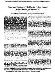
Example: Consider the practical example (as in [1]), with qp=5, and fp=86[kHz], of the 2nd-order current-mode LP filter in the first row and right column in Table 1. A sensitivity analysis for various designs of the current-mode LP filter is presented in what follows. Filters with various resistance (r) and capacitance (ρ) ratios are presented in Table 2 (they have an identical passive RC network as the voltage-mode filter examples researched in [1]). Corresponding Monte Carlo runs of the magnitudes of the current TF I(s)=IOUT(s)/IIN(s) with 1% Gaussiandistribution, zero-mean resistors and capacitors were carried out using PSpice and are presented in Fig. 6. A simple CCS component “F” in PSpice, was used to model an ideal current amplifier. In Fig. 6 circuit no. 3), and even more no. 4), have reduced sensitivities.
C1=C R1=R ρ R3=R 1+ρ
VOUT
2
+α
IIN 3 IIN
3
+β
VOUT
+α
IIN
1
1
VOUT
R2=rR
4
Twin-T
C2=C/ρ
2
R2=ρR C3=C(1+1/ρ)
3 IIN
3
+β
+β
+α
IIN
VOUT IIN
R1=R
3
2
R2=rR
+α
R2=rR
R =R ||R =R C2=C/ρ C 1=C 1a 1b IOUT 1
3 IIN
3
3
C1=C
C1=C IOUT
C =C/ρ 2 2
4
C2=C/ρ
the next stage
R1=R IOUT
R2=rR
2
4
4
3
Current-Based Biquads
4 C2=C/ρ
2
4
3 IIN
3
C2=C/ρ 4
3
R1=R1a||R1b=R BP- r=ρ>>1 Type (or min V IN Ba GSP).
V3
CURRENT TRANSFORMED CLASS-4 ACTIVE-RC BIQUADS, WITH DESIGN PARAMETERS FOR LOW-SENSITIVITY FILTERS.
Type Design
LP
3 +β
V2
s23
An exhaustive classification, which includes all possible current-based single-amplifier biquads, and which is derived from a similar voltage-based classification, is given in [11]. We restrict ourselves to the class-4 networks in [11], and the new design method based on the method in [1], will be applied to the design of low-sensitivity current-mode circuits. In this section we will directly transform the previously sensitivity-optimized voltagebased filters into current-based filters using transposition.
r=1; (or min VIN GSP), ρ>>1
t12
Figure 3. SFG of voltage-based Biquad.
LOW-SENSITIVITY CURRENT-MODE FILTERS
TABLE I.
2
V1
2
4
4
C2=C/ρ
R1a R1b
1
3 Twin-T
R2=ρR C3=C(1+1/ρ) 4 3
C1=C
1 IOUT
R1=R ρ R3=R 1+ρ
a. The name is according to [12]. In [12] is also presented 2nd-order BP filter type A. In [13] is shown that BP filter type A has higher sensitivity than BP filter type B.
3305
Figure 6. Monte Carlo runs of impedance-tapered current-mode 2nd-order LP filters given in Table 2. COMPONENT VALUES OF 2 -ORDER CURRENT MODE LP FILTER AS IN FIRST ROW OF TABLE 1. (RS IN [KΩ], CS IN [PF]).
TABLE II.
Filter Imp.-Tapered Non-Tapered C-Tap. min. GSP Partially-Tap. (r=1)
R1 R2 r C1 3.7 14.8 4 500 3.7 3.7 1 500 5.4 10 1.85 500 7.4 7.4 1 500
C2 125 500 125 125
ρ 4 1 4 4
V1
β 2.05 2.8 1.58 1.4
equivalent
No. 1) 2) 3) 4)
ND
I1
+α
I2
V2
I1
I2
A→∞ R2
(a)
R1 (b)
Figure 7. (a) Opamp-based non-inverting amplifier. (b) Possible singleinput, single-output current amplifier.
Other benefits of current mode-circuits (such as easier realization on an IC and wider operating bandwidth, etc.) are retained, whereas, additionally, their passive sensitivity is reduced.
REFERENCES [1]
[2] [3] [4]
[5] [6]
[7]
[8]
[9] [10] [11]
CONCLUSIONS
The connection between well-known active-RC voltage-mode filters and current-mode filters is provided. Note that in adjoint networks, the passive RC networks remain the same as those in the original network. Therefore, the circuits in [1][13][14], are good candidates for conversion to the current domain, owing to their low sensitivities to component tolerances. The new design procedure of current-mode filters using impedance tapering adds nothing to the cost of the derived circuits, only the component values must be judiciously chosen.
transposed
R2 A→∞
V1
The results of the MC analysis in Fig. 6 are identical to those for the voltage-mode LP circuit in the corresponding example given in [1]. Thus, for the design of the low-sensitivity LP filter capacitive impedance tapering with equal resistors (r=1), or resistor values selected for GSP minimization, provides current-mode circuits with min. sensitivity to the component tolerances [1]. The strategy of desensitization to component tolerances using impedance tapering for all allpole filters (for HP and BP according to the results in [13]), and for biquads with finite zeros using potential-symmetry of a Twin-T (according to [14]) is provided in the second column of Table 1. The sensitivity of those filters realized in the current domain has also been investigated using MC runs. The obtained results confirmed all design strategies of the circuits in Table 1, (note that high impedance sections of the passive network are inside a rectangle). In recent years a number of new active devices have been proposed to overcome the limitations of conventional opamps. In [5] the design of a current opamp is presented, using current conveyors, which does not exhibit a GB trade-off. A comprehensive classification of all operational amplifiers and current conveyors known from the literature is presented in [15], in the form of nine basic and fundamentally different opamps. An explanation is given which pairs of amplifiers are mutually reciprocal (and can be used in the process of deriving transposed filter circuits), while some of them are self-reciprocal. It is shown how all of them can be implemented in CMOS using only a few basic transistor building blocks. As an example, a typical non-inverting opamp voltage amplifier, which realizes the gain β=1+R2/R1 of the class-4 filters, and its adjoint current amplifier with identical gain are shown in Fig. 7 [7][15]. Note that the latter is implemented with current mirrors, which sense and copy the supply currents of the whole opamp (since any current flowing into the opamp must flow through opamp supplies). The circuits in Fig. 7 at least permit a laboratory comparison between current and voltage circuits to be made.
IV.
R1
V2
+β
[12] [13]
[14]
[15]
3306
G. S. Moschytz, “Low-sensitivity, low-power, active-RC allpole filters using impedance tapering”, IEEE Trans. CAS—II, vol. 46, no. 8, pp. 1009-1026, Aug. 1999. G. S. Moschytz, Linear integrated networks: fundamentals, NY (Bell Labs Series): V. Nostrad Reinhold Co., 1974. J. L. Bordewijk, “Inter-reciprocity applied to electrical networks”, Appl. Sci. Res. B6, pp. 1-74, 1956. S. W. Director, and A. W. Rohrer, “The generalized adjoint network and network sensitivities”, IEEE Trans. Circ. Theory, vol. 16, no. 3, pp. 318-323, Aug. 1969. G. W. Roberts and A. S. Sedra, “All current-mode frequency selective circuits”, Electronic Leters, vol. 25, pp. 759-761, 1989. G. W. Roberts and A. S. Sedra, “A general class of current amplifierbased biquadratic filter circuits”, IEEE Trans CAS-I, vol. 39, no. 4, pp. 257-263, April 1992. A. Carlosena and G. S. Moschytz, “Nullators and norators in voltage to current mode transformations”, Int. J. Circ. Theor. Appl., vol. 21, no. 4, pp. 421-424, July 1993. G. S. Moschytz, “Deriving current-mode circuits (filters) from voltage-mode circuits (filters),” in course Analog signal processing and related bipolar and CMOS circuit design, CEI-Europe, Advanced technology education, Sweden. C. A. Desoer and E. S. Kuh, Basic circuit theory, New York: McGraw-Hill, 1969, ch. 16. H. Schmid, “Circuit transposition using signal-flow graphs,” In Proc. ISCAS, Phoenix, USA, May 2002, vol. 2, pp. 25-28. G. S. Moschytz and A. Carlosena, “A classification of current-mode SABs based on voltage-to-current transformation,” IEEE Trans CASII, vol. 41, no. 2, pp. 151-156, Feb. 1994. G. S. Moschytz, Linear integrated networks: design, New York (Bell Labs Series): Van Nostrad Reinhold Co., 1975. D. Jurisic, G. S. Moschytz and N. Mijat, “Low-sensitivity active-RC high- and band-pass second-order sallen & key allpole filters”, In Proc. ISCAS, Phoenix, USA, May 2002, vol. 4. pp. 241-244. D. Jurisic, G. S. Moschytz and N. Mijat, “Low-sensitivity active-RC filters using impedance tapering of symmetrical bridged-T and twin-T networks”, In Proc. ISCAS, Kobe, Japan, May 2005. H. Schmid, “Approximating the universal active element,” IEEE Trans CAS-II, vol. 47, no. 11, pp. 1160-1169, Nov. 2000.