This article has been accepted for publication in a future issue of this journal, but has not been fully edited. Content may change prior to final publication. Citation information: DOI 10.1109/JXCDC.2017.2669213, IEEE Journal on Exploratory Solid-State Computational Devices and Circuits
IEEE JOURNAL OF EXPLORATORY SOLID-STATE COMPUTATIONAL DEVICES AND CIRCUITS
1
Non-Volatile Spintronic Memory Array Performance Benchmarking based on ThreeTerminal Memory Cell Chenyun Pan, Member, IEEE, and Azad Naeemi, Senior Member, IEEE
Abstract—For the conventional spin torque transfer random access memory (STT-RAM), trade-offs exist between read margin and write energy because both read and write currents pass through the same magnetic tunnel junction (MTJ). To improve the read/write performance and reduce the read disturb rate, threeterminal memory cell structures are investigated and the tradeoffs among read and write performance metrics are explored. A uniform memory array-level benchmarking is performed to compare various spintronic write mechanisms, including spin diffusion, spin Hall effect (SHE), domain wall motion, and magnetoelectric effect. Results show that three-terminal memory cells have the advantage of a small write energy dissipation, and up to two orders of magnitude reduction in the energy-delay product (EDP) is projected for the domain wall and magnetoelectric-based memory cells. Index Terms—Spintronic memory, spin diffusion, spin Hall effect, domain wall, magnetoelectric, performance modeling, read disturb rate.
I. INTRODUCTION
S
PIN transfer torque random access memory (STT-RAM) is one of the promising candidates for the non-volatile memory [1-3]. An STT-RAM cell stores data in the free magnet layer of a magnetic tunnel junction (MTJ). If the magnetization of the free magnet in the MTJ is in the same direction as that of the fixed magnet, the cell has a parallel configuration and a small resistance; if the magnetization of the free magnet is in the opposite direction, the cell has a large resistance. The resistance difference can be sensed by passing a bias current and comparing the voltage with a reference MTJ through a sense amplifier [4]. Several proposals have shown the implementation and benefits of using STT-RAM as the on-chip cache replacement thanks to its high density, low standby power, and competitive latency and endurance [5, 6]. Other studies also show its application as the main memory to achieve a small energy dissipation [7]. The non-volatility of STT-RAM enables a wide range of applications in the non-volatile computing [8]. It is crucial to minimize the energy for read and
Manuscript received August 1, 2016; revised January 10, 2017. This work was supported by the Semiconductor Research Corporation (SRC) NRI Theme 2624.001. C. Pan, and A. Naeemi are with the School of Electrical and Computer Engineering, Georgia Institute of Technology, Atlanta, GA 30332 USA (e-mail:
[email protected]).
write access due to the limited power supply for the energyharvesting applications [9]. One of the challenges of STT-RAM is the large critical current required to switch the magnetization of a magnet. Since both read and write currents pass through the same MTJ, trade-offs exist between read disturb rate and write energy. From the previous experimental work, the tunneling magnetoresistance (TMR) ratio of an MTJ increases with its tunneling oxide thickness [10]. Therefore, for a good memory array-level performance the oxide thickness needs to be sufficiently thick to achieve 1) a large TMR ratio that creates a voltage swing sensible by a sense amplifier, and 2) a small read current that lowers the read disturb rate. However, as the oxide thickness increases, the MTJ resistance rises. Hence, during the write operation, the write energy associated with the Joule heating in the MTJ and the access transistor increases significantly. To improve the read and write performance and reduce the read disturb rate, three-terminal memory cells have been studied based on the spin Hall effect (SHE), domain wall motion, and magnetostrictive effect [5, 6, 11-13]. In this work, for the first time, a variety of spintronic memory arrays with different current- and voltage-based writing mechanisms are investigated and compared in a uniform way, covering the spin diffusion, SHE, domain wall motion, and magnetoelectric effect. Compact analytical models are developed to optimize the array-level read and write performance in an efficient way. Optimal design parameters, such as the tunneling oxide thickness of MTJs and their write voltage, are obtained to achieve the minimum energy-delay product (EDP) during read and write operations under certain constraints, including minimum sensing swing and read disturb rate. Various TMR ratios of MTJs are also studied to quantify the potential read performance improvement. In addition, comparisons are made between the three-terminal spintronic memory and the conventional STT-RAM at array-level performance metrics, including delay and energy per read/write operation, read disturb rate, memory density, and fabrication complexity. The impact of the MTJ process variation on the read and write performance is also investigated. The rest of the paper is organized as follows. Section II illustrates the structure and layout of the three-terminal spintronic memory cell. Section III describes the read and write performance modeling approaches. Section IV shows the performance comparison and optimization of read/write operation in terms of delay, energy, and read disturb rate for a
2329-9231 (c) 2016 IEEE. Translations and content mining are permitted for academic research only. Personal use is also permitted, but republication/redistribution requires IEEE permission. See http://www.ieee.org/publications_standards/publications/rights/index.html for more information.
This article has been accepted for publication in a future issue of this journal, but has not been fully edited. Content may change prior to final publication. Citation information: DOI 10.1109/JXCDC.2017.2669213, IEEE Journal on Exploratory Solid-State Computational Devices and Circuits
IEEE JOURNAL OF EXPLORATORY SOLID-STATE COMPUTATIONAL DEVICES AND CIRCUITS variety of spintronic writing mechanisms. Conclusions are summarized in Section V. II. THREE-TERMINAL MEMORY CELL IMPLEMENTATION
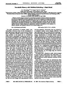
RBL
WBL
RWL
RWL WWL
BL
Fig. 1 shows schematics of spintronic memory cells based on four writing mechanisms: spin diffusion, SHE, domain wall motion, and magnetoelectric effect. By separating read and write paths, the write energy is reduced because the write current does not pass through the resistive MTJ. In addition, an MTJ with a thick oxide is used to reduce the read current and read disturb rate at a given read voltage without sacrificing the write energy. Furthermore, a thick tunneling oxide leads to a large TMR and resistance-area ratio, and potentially improves the sensing margin because the resistance is dominated by the MTJ instead of the resistances of the interconnects and the pass transistor. These benefits come from the extra terminal that is dedicated to the write operation. For the current-driven spintronic memory cells, an additional transistor is also required to isolate the read and write current paths and avoid sneak paths. For the voltage-controlled magnetoelectric memory cell, the insulating antiferromagnet layer separates the read and write current paths; therefore, a single access transistor is adequate. As a result, the footprint area for current-driven memory cells is 50% larger than those in the conventional STT-RAM and voltage-controlled magnetoelectric memory cells. Fig. 2 shows the layout and cross-sectional views of various types of spintronic memories. For the conventional STT-RAM and voltage-controlled spintronic memory cell, a two-finger transistor design is used to provide a large driving capability.
WWL
->
->
-> ->
SL
Spin Diffusion
WBL
SL
Spin Hall Effect
RBL
RBL WL
SL STT-RAM
RWL
WWL
WBL SL
SL
Magnetoelectric
Domain Wall Motion Copper
Fixed Magnet
Oxide
Spin Hall Effect Material
Free Magnet
Antiferromagnet
Fig. 1. Schematic of various spintronic memory categories being investigated, including spin diffusion, spin Hall effect, domain wall motion, and magnetoelectric effect.
The current-driven three-terminal memory cell has 50% larger footprint area than the conventional STT-RAM, where 𝐹 is equal to the half metal pitch of 30 nm. Fig. 2 (d) and (e) are cross-sectional views at dash lines A and B for the voltagecontrolled memory cell in Fig. 2 (c). For the current-driven spintronic memory cell shown in Fig. 2 (b), the cross-sectional views at dash line A for different writing mechanisms are
4F
F = half metal pitch
SL
4F
RBL WBL
4F BL
RBL
WBL
2
RBL SL
SL
SL
WBL
WBL
RWL WL
WL 6F WWL SL
WL
WL
Cross-section @ A
Cross-section @ B
3-Terminal VoltageControlled Memory Cell
Magnetoelectric
Magnetoelectric
(c)
(d)
A
3-Terminal CurrentDriven Memory Cell
(a)
WL
WL
A
Conventional STT
RBL
B
4F
4F
(b) WBL
WBL
(e) SHE Matel
WBL
Fixed Magnet SL
SL
SL
Free Magnet Antiferromagnet Oxide
RWL
WWL
RWL
WWL
RWL
WWL
Vias Copper
Cross-section @ A
Cross-section @ A
Spin Diffusion
Spin Hall Effect
(f)
(g)
Cross-section @ A
Active Layer
Domain Wall Motion
(h)
Fig. 2. Layout view of (a) conventional STT-RAM and (b) three-terminal spintronic memory cells. (c) and (d) show cross-sectional views at dash lines A and B, respectively, for a spin diffusion based memory cell. For other writing mechanisms, (e) – (g) show cross-sectional views at dash line B for spin Hall effect, domain wall motion, and magnetoelectric based memory cells, respectively.
2329-9231 (c) 2016 IEEE. Translations and content mining are permitted for academic research only. Personal use is also permitted, but republication/redistribution requires IEEE permission. See http://www.ieee.org/publications_standards/publications/rights/index.html for more information.
This article has been accepted for publication in a future issue of this journal, but has not been fully edited. Content may change prior to final publication. Citation information: DOI 10.1109/JXCDC.2017.2669213, IEEE Journal on Exploratory Solid-State Computational Devices and Circuits
IEEE JOURNAL OF EXPLORATORY SOLID-STATE COMPUTATIONAL DEVICES AND CIRCUITS shown in Fig. 2 (e) - (g). With an extra write terminal, the fabrication complexity increases. For instance, a two-terminal STT-RAM cell needs three lithography-etch steps and masks to accomplish vias to the transistor, MTJ stacks, and sourceline and bitline interconnects based on the 193 nm wavelength lithography technology; for a three-terminal cell, six lithography-etch steps and five masks are required. Therefore, with two more masks to create active layers and gates of transistors, the total number of masks increases from five to seven. From the layout views shown in Fig. 2 (a) - (c), the via density of the conventional STTRAM, three-terminal currentdriven memory, and the three-terminal voltage-driven memory are 208.3 μm-2, 231.5 μm-2, and 277.8 μm-2, respectively. III. MODELING APPROACHES A. Read Performance Modeling The read operations are identical for all types of memory cells. The MTJ read circuitry is adopted from the default sensing circuitry presented in the previous work [14]. The read delay can be estimated as 𝑡𝑟𝑒𝑎𝑑 = 𝑡𝑊𝐿 + 𝑡𝑠𝑒𝑛𝑠𝑒
(1)
where 𝑡𝑊𝐿 = 0.7𝑅𝑑𝑟𝑖𝑣𝑒 𝐶𝑊𝐿 + 0.4𝑅𝑊𝐿 𝐶𝑊𝐿 is the wordline delay, assuming it is driven by a 5×minimum-sized inverter (W = 20F), 𝑅𝑊𝐿 is the interconnect resistance, which takes into account the impact of size effects on Cu resistivity. The grain boundary reflectivity and the surface specularity are assumed to be 0.15 and 0, respectively [15], 𝐶𝑊𝐿 is the interconnect capacitance, and 𝑡𝑠𝑒𝑛𝑠𝑒 is the delay associated with the bitline charge or discharge as well as the sense amplifier delay that is simulated based on the SPICE simulation. The bitline capacitance in the simulation is 𝐶𝐵𝐿 = 𝑐𝑤 𝑙𝐵𝐿 + 𝐶𝑡𝑟𝑎𝑛 𝑁𝑏𝑖𝑡 , which includes both bitline capacitance and the transistor capacitance. The minimum required sensing voltage swing at the input of the sense amplifier is assumed to be 50 mV. The sense amplifier circuit is adopted from the previous work, and the CMOS device model follows the 16nm ASU PTM [16, 17]. The read energy is written as 𝐸𝑟𝑒𝑎𝑑 = 2𝑉𝑟𝑒𝑎𝑑 𝐼𝑏𝑖𝑎𝑠 𝑡𝑟𝑒𝑎𝑑 + 𝐸𝑊𝐿 + 𝐸𝑆𝐴
(2)
2 where 𝐸𝑊𝐿 = 0.5(𝐶𝑊𝐿 /𝑁𝑏𝑖𝑡 + 𝐶𝑡𝑟𝑎𝑛 )𝑉𝑟𝑒𝑎𝑑 is the switching energy per cell that is associated with wordline and pass transistor, 𝑁𝑏𝑖𝑡 is the number of bits in a row/column, 𝑉𝑟𝑒𝑎𝑑 is the read voltage of 1V, 𝐼𝑏𝑖𝑎𝑠 is the average read current from the SPICE simulation, 𝐶𝑅𝐵𝐿 is the read bitline capacitance, and 𝐸𝑆𝐴 = 𝑃𝑆𝐴 𝑡𝑟𝑒𝑎𝑑 is the sense amplifier energy based on the SPICE simulation. The read disturb rate is calculated as [18]
𝑃 = 1 − exp (− where 𝜏1 = 𝜏0 exp (
Δ𝐸 𝑘𝐵 𝑇
(1 −
𝐼𝑟𝑒𝑎𝑑 𝐼𝑐
𝑡𝑟𝑒𝑎𝑑 ) 𝜏1
(3)
)), 𝜏0 is the attempt period
of 1 ns [18], Δ𝐸 is the thermal stability factor, 𝐼𝑟𝑒𝑎𝑑 is the read bias current, 𝑡𝑟𝑒𝑎𝑑 is the read delay, and 𝐼𝑐 is the critical charge
3
current to switch the magnet, which is estimated by following Nikonov’s work [19]. TABLE I lists the simulation parameters and assumptions, including properties of the in-plane magnet anisotropy (IMA) and the perpendicular magnet anisotropy (PMA) materials. The resistance-area product and the baseline TMR ratio for MTJs with various oxide thicknesses are taken from the previous experimental work [10]. Since the maximum TMR observed in the experimental work is 604% at room temperature [20], MTJs with up to 4×of the baseline TMR (maximum ~150% [10]) are investigated in this paper. TABLE I MEMORY ARRAY AND CELL DESIGN PARAMETER AND CONFIGURATION Parameters Half Metal Pitch F (nm) Array Size (bit) CMOS Driving Voltage Vread (V) Transistor Resistance W = 60nm (KΩ) Transistor Capacitance @ W = 60nm (aF) Interconnect Capacitance (fF/µm) Bitline Resistance (Ω/µm) Wordline Resistance (Ω/µm) Damping Coefficient α IMA Saturation Magnetization Ms (A/m) PMA Saturation Magnetization Ms (A/m) Perpendicular Anisotropy Ku (J/m3) IMA Magnet Dimension (nm3) PMA Magnet Dimension (nm3) Thermal Barrier Eb (kBT) Spin Hall angle θ Spin Injection Coefficient β
Values 30 1000×1000 1 5 60 0.15 20.5 53 0.01 106 3×10⁵ 6×10⁴ 15×45×4 30×30×4.6 60 0.3 0.5
B. Write Performance Modeling 1) Conventional STT Memory The write delay is dominated by the wordline delay and the magnet switching time, which is written as 𝑡𝑤𝑟𝑖𝑡𝑒 = 𝑡𝑊𝐿 + 𝑡𝐵𝐿 + 𝑡𝑚𝑎𝑔 ,
(4)
where 𝑡𝑊𝐿 is the wordline delay used in the read delay (1), 𝑡𝐵𝐿 is the bitline delay, and 𝑡𝑚𝑎𝑔 is the magnet switching time following Nikonov’s work [19], which is written as 𝑡𝑚𝑎𝑔 =
𝑀𝑠 𝑉𝑒 𝜋 ln ( ) 𝜇𝐵 (𝐼𝑠 − 𝐼𝑐 ) 2√𝑘𝐵 𝑇/2𝐸𝑏
(5)
where 𝑀𝑠 is the saturation magnetization, 𝑉 is the volume of the magnet, 𝑒 is the elementary charge, 𝜇𝐵 is the Bohr magneton, 𝐸𝑏 is the thermal barrier, 𝐼𝑐 is the critical switching current of a magnet based on [19], 𝐼𝑠 = 𝛽 ∙ 𝐼𝑤𝑟𝑖𝑡𝑒 is the spinpolarized current, 𝐼𝑤𝑟𝑖𝑡𝑒 = 𝑉𝑤𝑟𝑖𝑡𝑒 /(𝑅𝐵𝐿 + 𝑅𝑆𝐿 + 𝑅𝑀𝑇𝐽 + 𝑅𝑡𝑟𝑎𝑛 ) is the write charge current, 𝑉𝑤𝑟𝑖𝑡𝑒 is the write voltage applied on the write bitline at the edge of the memory array, 𝛽 is the spin injection coefficient, 𝑅𝑀𝑇𝐽 is the average resistance of parallel and antiparallel configurations, which are obtained based on the experimental data [10]. Here, a PMA magnet is used based on the assumptions listed in TABLE I. The write energy is expressed as
2329-9231 (c) 2016 IEEE. Translations and content mining are permitted for academic research only. Personal use is also permitted, but republication/redistribution requires IEEE permission. See http://www.ieee.org/publications_standards/publications/rights/index.html for more information.
This article has been accepted for publication in a future issue of this journal, but has not been fully edited. Content may change prior to final publication. Citation information: DOI 10.1109/JXCDC.2017.2669213, IEEE Journal on Exploratory Solid-State Computational Devices and Circuits
IEEE JOURNAL OF EXPLORATORY SOLID-STATE COMPUTATIONAL DEVICES AND CIRCUITS 2 𝐸𝑤𝑟𝑖𝑡𝑒 = 𝐼𝑤𝑟𝑖𝑡𝑒 (𝑅𝐵𝐿 + 𝑅𝑆𝐿 + 𝑅𝑡𝑟𝑎𝑛 + 𝑅𝑀𝑇𝐽 ) ∙ 𝑡𝑚𝑎𝑔 2 2 + 0.5𝐶𝑊𝐿 𝑉𝑐𝑚𝑜𝑠 + 0.5𝐶𝐵𝐿 𝑉𝑤𝑟𝑖𝑡𝑒
(6)
4
wall speed 𝑐𝑑𝑤 and the input current density is adopted from [24]. The write energy is adopted from (6) by replacing the MTJ resistance 𝑅𝑀𝑇𝐽 with the domain wall resistance 𝑅𝑑𝑤 of 200 Ω.
2) Spin Diffusion based Memory The basic writing mechanism is adopted from the all-spin logic proposed by Dutta et al. [21]. By applying a write voltage to the input magnet on the left, the current passing through the magnet gets polarized, generating spin-polarized currents that diffuse to the ground and the free magnet on the right. These two spin-polarized currents satisfy the spin diffusion equation 𝜕 2 𝜇𝑠 /𝜕𝑥 2 = 𝜇𝑠 /𝑙𝑠𝑓 and 𝐽𝑠 = 𝜎/𝑒 ∙ 𝜕𝜇𝑠 /𝜕𝑥 , where 𝜇𝑠 is the spin accumulation, 𝐽𝑠 is the spin-polarized current density, 𝑙𝑠𝑓 is the spin relaxation length of 400 nm, 𝜎 is the interconnect conductivity, and 𝑒 is the elementary charge. Boundary conditions are as follows: the spin accumulation at the output magnet is zero, and the input spin-polarized current is 𝛽 ∙ 𝐼𝑤𝑟𝑖𝑡𝑒 , where 𝐼𝑤𝑟𝑖𝑡𝑒 is the charge current, and 𝛽 is the spin injection coefficient. By solving the equations and associated boundary conditions, the spin-polarized current received at the output magnet is derived as
5) Magnetoelectric based Memory Instead of using STT as the writing mechanism, magnetoelectric-based spintronics are promising candidates for the memory application because of its voltage-control property [25]. For a given write voltage, the electric field is calculated by 𝐸𝑚𝑒 = 𝑉𝑤𝑟𝑖𝑡𝑒 /𝑡𝑚𝑒 , where 𝑡𝑚𝑒 is the thickness of the magnetoelectric material at a value of 2 nm. The corresponding magnetic field applied on the magnet due to the exchange bias effect follows Nikonov’s work [19] and is estimated as 𝐻𝑎𝑝𝑝 = (𝐵𝑚𝑒 /𝐸𝑐 𝜇0 )𝐸𝑚𝑒 , where the critical field EC = 2.6 MV/m, and the magnetoelectric exchange bias field Bme = 9 mT, giving an ME coefficient of 3.26 ns/m. The magnet switching time 𝑡𝑚𝑎𝑔 is simulated by solving the LLG equation with a free magnet dimension of 90×30×2 nm3. The write delay is written as
𝛽𝐼𝑤𝑟𝑖𝑡𝑒
where the 𝐶𝐴𝐹𝑀 is the capacitance of antiferromagnet material at a dielectric constant of 13 [19]. The energy dissipation is calculated as
𝐼𝑠 =
sinh(𝑙𝑐 /𝑙𝑠𝑓 ) cosh(𝑙𝑔 /𝑙𝑠𝑓 ) sinh(𝑙𝑔 /𝑙𝑠𝑓 )
+ cosh(𝑙𝑐 /𝑙𝑠𝑓 )
(7)
where 𝑙𝑐 is the channel length of 4F, and 𝑙𝑔 is the length of the ground path. Two types of magnets are studied, including IMA and PMA material. The critical switching current and the corresponding switching delay are adopted from Nikonov’s work [19], and key assumptions are listed in TABLE I. Since the write current only flows through the magnet instead of the cell MTJ, 𝑅𝑀𝑇𝐽 in the write energy (6) is replaced by the ferromagnet resistance 𝑅𝑓 , which is much smaller than the MTJ resistance and leads to a major energy saving. 3) Spin Hall effect based Memory The basic writing mechanism is based on the spin Hall effect that converts charge currents into spin currents due to the spin orbital coupling [22]. The spin-polarized current density is 𝐽𝑠 = 𝐽𝑐 𝜃, where 𝜃 is the spin Hall angle at a value of 0.3 [23], and 𝐽𝑐 is the charge current density. For a given write voltage 𝑉𝑤𝑟𝑖𝑡𝑒 , the spin-polarized current 𝐼𝑠 is obtained, and the magnet switching time 𝑡𝑚𝑎𝑔 is estimated by (5). Equation (6) is used to calculate the write energy by replacing the MTJ resistance 𝑅𝑀𝑇𝐽 with 𝑅𝑆𝐻𝐸 , which is the SHE material resistance and has a value of 150 Ω. Here, IMA magnets are used, whose parameters are shown in TABLE I. Note that the spin orbital torque switching has only been experimentally demonstrated in a relatively large device. The predictive model used in this work assuming the device is scalable so that the potential performance is benchmarked against other spintronic memory devices. 4) Domain Wall Motion based Memory The basic writing mechanism is adopted from the mLogic in [24]. Data stored in the memory cell depends on the domain wall positions that are set according to the input voltage. The write delay follows (4) by replacing magnet switching time 𝑡𝑚𝑎𝑔 with 6𝐹/𝑐𝑑𝑤 , where 𝐹 is the minimum feature size, and 𝑐𝑑𝑤 is the domain wall speed. The relation between the domain
𝑡𝑤𝑟𝑖𝑡𝑒 = 𝑡𝑊𝐿 + 𝑡𝐵𝐿 + 0.7(𝑅𝐵𝐿 + 𝑅𝑡𝑟𝑎𝑛 )𝐶𝐴𝐹𝑀 + 𝑡𝑚𝑎𝑔
2 2 𝐸𝑤𝑟𝑖𝑡𝑒 = 0.5𝐶𝑊𝐿 𝑉𝑑𝑑 + 0.5(𝐶𝑊𝐵𝐿 + 𝐶𝐴𝐹𝑀 )𝑉𝑤𝑟𝑖𝑡𝑒
(8)
(9)
IV. SIMULATION RESULTS A. Read Performance Analysis Using the modeling approach developed in Section III, various performance metrics versus the tunneling oxide thickness are calculated as shown in Fig. 3. The baseline TMR ratio and three other TMR ratios are investigated to quantify the performance benefits of MTJs at larger TMR ratios. In Fig. 3 (a), the sensing voltage swing ΔV increases with the increase of the tunneling oxide thickness. The reasons are: 1) as the TMR ratio increases, the ON and OFF states of the MTJ are more distinguishable, and 2) the increase in the MTJ resistance reduces the bias current and suppresses the impact of the parasitic interconnect and transistor resistances. For a small oxide thickness, the read disturb rate, shown in Fig. 3 (b), is high because of the small sensing voltage swing and the large read bias current. As the oxide thickness increases, the read disturb rate decreases due to the smaller read current induced by the larger MTJ resistance. The read disturb rate saturates as the oxide thickness increases beyond a certain point because the significantly longer read time diminishes the benefit from the lower read current. Fig. 3 (c) shows that optimal oxide thicknesses exist to achieve the minimum read delay. When the oxide is thin, the increase in the oxide thickness improves the sensing voltage swing and reduces the RC delay required to reach the minimum sensing voltage of 50 mV. If the oxide thickness increases beyond a certain point, however, the TMR saturates, and the large MTJ resistance dominates the delay and increases the overall read delay. Another observation is that the memory at a
2329-9231 (c) 2016 IEEE. Translations and content mining are permitted for academic research only. Personal use is also permitted, but republication/redistribution requires IEEE permission. See http://www.ieee.org/publications_standards/publications/rights/index.html for more information.
This article has been accepted for publication in a future issue of this journal, but has not been fully edited. Content may change prior to final publication. Citation information: DOI 10.1109/JXCDC.2017.2669213, IEEE Journal on Exploratory Solid-State Computational Devices and Circuits
IEEE JOURNAL OF EXPLORATORY SOLID-STATE COMPUTATIONAL DEVICES AND CIRCUITS
5
large TMR (green curves) provides a small delay for an MTJ with a thin oxide, but it causes a large delay for the one with a thick oxide. This is because at a thin oxide, the sensing voltage swing is small and a large TMR helps to reduce the read delay, but for a thick oxide, the sensing voltage swing is large enough, and the large MTJ resistance at the OFF state increases the worst case read delay.
Fig. 4. Read energy versus read delay, where the red star shows the preferred corner.
Fig. 5. Normalized probability density function of EDP during the read operation for three TMR assumptions.
Fig. 3. (a) Sensing voltage swing, (b) read delay, (c) read disturb rate, and (d) read energy versus the tunneling oxide thickness for various TMR ratio relative to the experimental value. The top x axis shows the resistance-area product of an MTJ with a parallel configuration.
For the read energy shown in Fig. 3 (d), optimal tunneling oxide thicknesses exist to achieve the minimum energy. The reason is that if the oxide thickness is small, a large energy is dissipated because of 1) the large bias current due to a small MTJ resistance, and 2) the large read delay due to a limited sensing voltage swing; if the oxide thickness is large, the significant increase in the delay causes a jump in the leakage energy associated with the sense amplifier. Compared to the minimum delay design point, a thicker tunneling oxide is preferred to minimize the read energy. Fig. 4 shows the trade-offs between the read delay and read energy for memory cells using PMA magnets. The contour of read disturb rates is shown as purple dash lines, which decreases as the oxide thickness increases. One can observe that optimal oxide thicknesses exist to minimize the EDP for different TMR assumptions. One major design advantage of the three-terminal memory cell is that the performance trade-offs made in the read operation do not affect the write energy or delay because of the separation between the read and write current paths.
To investigate the impact of the process variation on the memory performance, Monte Carlo simulations are performed at the minimum EDP design point according to Fig. 4. Fig. 5 shows the normalized probability density function of the EDP for three TMR assumptions. The 3σ deviation is assumed to be 10% for the tunneling oxide thickness and the area of MTJs. Due to a small sensing margin, a low TMR memory cell is more sensitive to the process variation, leading to a large variability in terms of the overall EDP. This applies to both conventional STT-RAM and the three-terminal memory cells, since their read operations are identical. B. Write Performance Analysis Based on the assumptions and configurations illustrated in Section III, Fig. 6 shows the total write access energy and corresponding write voltage versus the total write access time. Note that the write voltage is the voltage applied on the write bitline at the edge of the memory array. The actual voltage across the MTJ, magnets, or the SHE material is a fraction of the write voltage due to the voltage drop across the select transistor and long bitline. The oxide thickness of the MTJ is set as 1.25 nm for the STT-RAM. By sweeping the write voltage, trade-offs between write energy and delay can be achieved. Optimal write voltages exist to reach the minimum EDP because 1) if the write voltage is high, the large writing current dramatically increases the energy associated with Joule heating, and 2) if the write voltage is low, the write current
2329-9231 (c) 2016 IEEE. Translations and content mining are permitted for academic research only. Personal use is also permitted, but republication/redistribution requires IEEE permission. See http://www.ieee.org/publications_standards/publications/rights/index.html for more information.
This article has been accepted for publication in a future issue of this journal, but has not been fully edited. Content may change prior to final publication. Citation information: DOI 10.1109/JXCDC.2017.2669213, IEEE Journal on Exploratory Solid-State Computational Devices and Circuits
IEEE JOURNAL OF EXPLORATORY SOLID-STATE COMPUTATIONAL DEVICES AND CIRCUITS approaches the critical switching current and increases the delay significantly.
6
because rather than switching the entire magnet, the domain wall position inside the magnet moves based on the direction of the input current. Therefore, it requires a lower write voltage and a lower current density than that of switching a whole magnet. Magnetoelectric-based memory cells also provide relatively small energy consumption thanks to its low voltage operation and the voltage-driven property. The minimum write voltage is set to be 100 mV due to the supply noise, which limits the domain wall motion and magnetoelectric based memory cell performance. For the reliability concern, the maximum current density reported in ITRS for the year 2026 is 4.5 MA/cm2 [26], which is higher than most of the memory cells shown in TABLE II, except for the spin diffusion based memory cell with IMA magnet because of the large charge current required to generate a spin-polarized current to switch the magnet. Note that the actual current density limits also depend on the duty cycle and material considerations. For the memory application, the average current density is expected to be smaller for memory blocks that are accessed less frequently. Here, the ITRS projection for the current limit is listed only as a reference. TABLE II PERFORMANCE COMPARISON FOR VARIOUS SPINTRONIC MEMORY CELLS Critical Charge EDPwrite Cell Vwrite Charge Current @ 3σ Area (V) Current Density on (ns·fJ) (F2)* (uA) BL(MA/cm2) 3764 4343 0.9 24 15.10 1.31 10215 40339 1.2 24 51.56 9.48 504 545 0.44 24 15.10 3.44 322 410 0.46 24 103.09 3.62 7.7 8.5 0.1 24 2.25 0.79 7.4 7.8 0.1 16 Voltage-Driven
Memory twrite Ewrite EDPwrite Type (ns) (fJ) (ns·fJ)
Fig. 6. (a) Total write access energy versus total write access time for various types of spintronic memory cells using different write voltages, where red star shows the preferred performance corner. The write energy includes the Joule heating and switching energy of MTJ, transistors, and interconnects. (b) The write voltage versus the total write access time. In the legend, SD, SHE, DW, and ME stand for spin diffusion, spin Hall effect, domain wall motion, and magnetoelectric-based memory cells, respectively.
Fig. 7. Write energy versus write delay for various types of spintronic memory cells at minimum EDP nominal design point without variation.
Fig. 7 shows the optimal write energy versus the write time at the optimal EDP design points. The detailed design parameters and performance metrics are listed in TABLE II, where the fifth column takes into account the variation of the thermal barrier with a 3σ deviation of 10%. One can observe that the domain wall based memory cell provides the best EDP
STT SD-IMA SD-PMA SHE DM ME
12.6 7.4 4.7 3.7 2.7 6.5
299 1373 107 88 2.8 1.1
* F = half metal pitch TABLE III DELAY AND ENERGY BREAKDOWN FOR VARIOUS SPINTRONIC MEMORY CELLS Memory Type
tmag (ns)
tBL (ns)
tWL (ns)
Ejoule (fJ)
EBL (fJ)
EWL (FJ)
STT SD-IMA SD-PMA SHE DM ME
7.46 5.89 3.15 2.10 1.17 5.57
4.40 0.82 0.82 0.82 0.82 0.73
0.73 0.73 0.73 0.73 0.73 0.73
207.48 1204.75 84.90 63.74 1.62 0.001
91.61 168.34 22.15 24.51 1.17 1.08
0.054 0.054 0.054 0.054 0.054 0.054
TABLE III shows the delay and energy breakdown for each spintronic memory technology, where 𝐸𝑗𝑜𝑢𝑙𝑒 is associated with the Joule heating of the interconnects and selecting transistors, and for the magnetoelectric-based memory, 𝐸𝑗𝑜𝑢𝑙𝑒 is the dynamic switching energy of the antiferroelectric material, and 𝐸𝐵𝐿 and 𝐸𝑊𝐿 are the switching energy of the bitlines and wordlines. From the data shown in TABLE III, the majority of the energy for the current-driven spintronic memory comes from the Joule heating. For the voltage-controlled magnetoelectric-based memory, the energy is dominated by the switching energy of the bitlines. For various spintronic memory, the majority of the delay is contributed by the switching time of the magnets.
2329-9231 (c) 2016 IEEE. Translations and content mining are permitted for academic research only. Personal use is also permitted, but republication/redistribution requires IEEE permission. See http://www.ieee.org/publications_standards/publications/rights/index.html for more information.
This article has been accepted for publication in a future issue of this journal, but has not been fully edited. Content may change prior to final publication. Citation information: DOI 10.1109/JXCDC.2017.2669213, IEEE Journal on Exploratory Solid-State Computational Devices and Circuits
IEEE JOURNAL OF EXPLORATORY SOLID-STATE COMPUTATIONAL DEVICES AND CIRCUITS
TABLE IV PROCESSING REQUIREMENT AND CRITICAL PARAMETERS FOR VARIOUS MEMORY TECHNOLOGIES
[4]
Processing Requirement and Desired Parameters
[5]
Memory Technology Conventional STTRAM
Write Operation
Read Operation
MTJs with a large TMR and a moderate RA. Preferred RA would be smaller compared to the three-terminal memory because of the trade-off between read and write energy.
Spin Diffusion
Large spin polarization factor β
Spin Hall
Large spin Hall angle θ
Domain Wall
Small critical depinning current
Magnetoelectric
Large magnetoelectric coefficient
[6]
[7] MTJs with a large TMR and a moderate RA
[8]
[9]
To further improve the spintronic memory performance in terms of write/read delay and energy, TABLE IV lists the processing requirement and critical parameters for each memory technology. For the conventional STTRAM, since the read and write operation share the same MTJ, the MTJ with a large TMR is preferred so that the oxide thickness can be reduced to achieve a small RA, which subsequently lowers the read and write energy. For the three-terminal spintronic memory, the write operation is decoupled from the read operation and can be improved as described in TABLE IV.
[10]
[11]
[12]
[13]
V. CONCLUSION This paper studies the three-terminal non-volatile spintronic memory cells. Read and write performance is examined at the array level using a variety of current- and voltage-based writing mechanisms, including spin diffusion, SHE, domain wall motion, and magnetoelectric effect. Compact memory layouts and structures are developed, and trade-offs are explored among key performance metrics, such as read/write energy/delay and read disturb rate. Compared to the conventional STT-RAM, three-terminal cells have smaller energy dissipation because of their separate read and write current paths. The domain wall based memory cell provides the smallest EDP due to its lowest critical current.
[14]
ACKNOWLEDGEMENT
[19]
The authors would like to thank Steve Kramer, Loris Vendrame, Marco Sforzin from Micron Technology for the useful discussions and insightful inputs for this work.
[20]
[15]
[16] [17] [18]
REFERENCE [1]
[2]
[3]
E. Chen, D. Apalkov, Z. Diao, A. Driskill-Smith, D. Druist, D. Lottis, et al., "Advances and future prospects of spin-transfer torque random access memory," Magnetics, IEEE Transactions on, vol. 46, pp. 1873-1878, 2010. Z. Diao, Z. Li, S. Wang, Y. Ding, A. Panchula, E. Chen, et al., "Spintransfer torque switching in magnetic tunnel junctions and spin-transfer torque random access memory," Journal of Physics: Condensed Matter, vol. 19, p. 165209, 2007. M. Hosomi, H. Yamagishi, T. Yamamoto, K. Bessho, Y. Higo, K. Yamane, et al., "A novel nonvolatile memory with spin torque transfer
[21]
[22] [23]
[24]
7
magnetization switching: Spin-RAM," in International Electron Devices Meeting, 2005, pp. 459-462. C. W. Smullen, V. Mohan, A. Nigam, S. Gurumurthi, and M. R. Stan, "Relaxing non-volatility for fast and energy-efficient STT-RAM caches," in High Performance Computer Architecture (HPCA), 2011 IEEE 17th International Symposium on, 2011, pp. 50-61. K. Wang, J. Alzate, and P. K. Amiri, "Low-power non-volatile spintronic memory: STT-RAM and beyond," Journal of Physics D: Applied Physics, vol. 46, p. 074003, 2013. J. Kim, A. Paul, P. A. Crowell, S. J. Koester, S. S. Sapatnekar, J.-P. Wang, et al., "Spin-based computing: Device concepts, current status, and a case study on a high-performance microprocessor," Proceedings of the IEEE, vol. 103, pp. 106-130, 2015. E. Kultursay, M. Kandemir, A. Sivasubramaniam, and O. Mutlu, "Evaluating STT-RAM as an energy-efficient main memory alternative," in Performance Analysis of Systems and Software (ISPASS), 2013 IEEE International Symposium on, 2013, pp. 256-267. K. Ma, Y. Zheng, S. Li, K. Swaminathan, X. Li, Y. Liu, et al., "Architecture exploration for ambient energy harvesting nonvolatile processors," in High Performance Computer Architecture (HPCA), 2015 IEEE 21st International Symposium on, 2015, pp. 526-537. A. P. Chandrakasan, D. C. Daly, J. Kwong, and Y. K. Ramadass, "Next generation micro-power systems," in VLSI Circuits, 2008 IEEE Symposium on, 2008, pp. 2-5. S. Yuasa, T. Nagahama, A. Fukushima, Y. Suzuki, and K. Ando, "Giant room-temperature magnetoresistance in single-crystal Fe/MgO/Fe magnetic tunnel junctions," Nature materials, vol. 3, pp. 868-871, 2004. R. Venkatesan, M. Sharad, K. Roy, and A. Raghunathan, "DWMTAPESTRI-an energy efficient all-spin cache using domain wall shift based writes," in Proceedings of the Conference on Design, Automation and Test in Europe, 2013, pp. 1825-1830. A. Khan, D. E. Nikonov, S. Manipatruni, T. Ghani, and I. A. Young, "Voltage induced magnetostrictive switching of nanomagnets: Strain assisted strain transfer torque random access memory," Applied Physics Letters, vol. 104, p. 262407, 2014. S. Manipatruni, D. E. Nikonov, and I. A. Young, "Energy-delay performance of giant spin Hall effect switching for dense magnetic memory," Applied Physics Express, vol. 7, p. 103001, 2014. M. Jefremow, T. Kern, W. Allers, C. Peters, J. Otterstedt, O. Bahlous, et al., "Time-differential sense amplifier for sub-80mV bitline voltage embedded STT-MRAM in 40nm CMOS," in Solid-State Circuits Conference Digest of Technical Papers (ISSCC), 2013 IEEE International, 2013, pp. 216-217. C. Pan and A. Naeemi, "A Proposal for a Novel Hybrid Interconnect Technology for the End of Roadmap," Electron Device Letters, IEEE, vol. 35, pp. 250-252, 2014. N. Muralimanohar, R. Balasubramonian, and N. P. Jouppi, "CACTI 6.0: A tool to model large caches," HP Laboratories, pp. 22-31, 2009. Predictive Technology Model (PTM), available online at http://ptm.asu.edu, 2012. L.-B. Faber, W. Zhao, J.-O. Klein, T. Devolder, and C. Chappert, "Dynamic compact model of spin-transfer torque based magnetic tunnel junction (MTJ)," in Design & Technology of Integrated Systems in Nanoscal Era, 2009. DTIS'09. 4th International Conference on, 2009, pp. 130-135. D. E. Nikonov and I. A. Young, "Benchmarking of Beyond-CMOS Exploratory Devices for Logic Integrated Circuits," Exploratory SolidState Computational Devices and Circuits, IEEE Journal on, vol. 1, pp. 3-11, 2015. S. Ikeda, J. Hayakawa, Y. Ashizawa, Y. Lee, K. Miura, H. Hasegawa, et al., "Tunnel magnetoresistance of 604% at 300 K by suppression of Ta diffusion in CoFeB/MgO/CoFeB pseudo-spin-valves annealed at high temperature," Applied Physics Letters, vol. 93, p. 2508, 2008. B. Behin-Aein, D. Datta, S. Salahuddin, and S. Datta, "Proposal for an allspin logic device with built-in memory," Nature nanotechnology, vol. 5, pp. 266-270, 2010. A. Hoffmann, "Spin Hall effects in metals," Magnetics, IEEE Transactions on, vol. 49, pp. 5172-5193, 2013. C.-F. Pai, L. Liu, Y. Li, H. Tseng, D. Ralph, and R. Buhrman, "Spin transfer torque devices utilizing the giant spin Hall effect of tungsten," Applied Physics Letters, vol. 101, p. 122404, 2012. D. Morris, D. Bromberg, J.-G. J. Zhu, and L. Pileggi, "mLogic: Ultra-low voltage non-volatile logic circuits using STT-MTJ devices," in Proceedings of the 49th Annual Design Automation Conference, 2012, pp. 486-491.
2329-9231 (c) 2016 IEEE. Translations and content mining are permitted for academic research only. Personal use is also permitted, but republication/redistribution requires IEEE permission. See http://www.ieee.org/publications_standards/publications/rights/index.html for more information.
This article has been accepted for publication in a future issue of this journal, but has not been fully edited. Content may change prior to final publication. Citation information: DOI 10.1109/JXCDC.2017.2669213, IEEE Journal on Exploratory Solid-State Computational Devices and Circuits
IEEE JOURNAL OF EXPLORATORY SOLID-STATE COMPUTATIONAL DEVICES AND CIRCUITS
8
[25] W. Kleemann, "Magnetoelectric spintronics," Journal of Applied Physics, vol. 114, p. 027013, 2013. [26] International Technology Roadmap for Semiconductors (ITRS), available online at http://www.itrs.net/, 2012.
2329-9231 (c) 2016 IEEE. Translations and content mining are permitted for academic research only. Personal use is also permitted, but republication/redistribution requires IEEE permission. See http://www.ieee.org/publications_standards/publications/rights/index.html for more information.