602
IEEE ELECTRON DEVICE LETTERS, VOL. 32, NO. 5, MAY 2011
Nonvolatile Memory by All-Around-Gate Junctionless Transistor Composed of Silicon Nanowire on Bulk Substrate Sung-Jin Choi, Dong-Il Moon, Sungho Kim, Jae-Hyuk Ahn, Jin-Seong Lee, Jee-Yeon Kim, and Yang-Kyu Choi
Abstract—A junctionless transistor with a width of 10 nm and a length of 50 nm is demonstrated for the first time. A silicon nanowire (SiNW) channel is completely surrounded by a gate, and the SiNW is built onto the bulk substrate. The proposed junctionless transistor is applied to a Flash memory device composed of oxide/nitride/oxide gate dielectrics. Acceptable memory characteristics are achieved regarding the endurance, data retention, and dc performance of the device. It can be expected that the inherent advantages of the junctionless transistor can overcome the scaling limitations in Flash memory. Hence, the junctionless transistor is a strong candidate for the further scaling of NAND Flash memory below the 20-nm node. Index Terms—All-around gate (AAG), Bosch process, bulk substrate, Flash memory, junctionless, junctionless field-effect transistor (FET), junctionless transistor, nanowire, silicon nanowire (SiNW), SONOS.
I. I NTRODUCTION
F
LASH memory (i.e., a type of nonvolatile memory) has scaled rapidly down to the 30-nm node [1]. However, many critical scaling limits are also rapidly foreshadowing no further downscaling, as reliance has mainly been on conventional approaches. Hence, a new and innovative device structure is urgently required [2]. Most importantly, the short-channel effects (SCEs) among the crucial limitations have increasingly become unavoidable technical challenges, as it is difficult to scale the equivalent oxide thickness (EOT) below 10 nm due to the nature of multilayered gate dielectrics. Shallow junctions are very important to suppress the SCEs; however, it is difficult to control the junction depth and profile precisely. Moreover, the formation of such shallow junctions becomes a serious concern in the future of 3-D multistacking integration due to the large thermal budget. For this reason, a “junction-free
Manuscript received December 28, 2010; accepted February 11, 2011. Date of current version April 27, 2011. This work was supported in part by the IT R&D program of MKE/KEIT (10035320, Development of novel 3-D stacked devices and core materials for the next generation Flash memory), by the IT R&D program of MKE/KEIT (10029953, Terabit Nonvolatile Memory Development), by the Nano R&D program through the National Research Foundation of Korea funded by the Ministry of Education, Science, and Technology under Grant 2009-0082583), and by the Samsung Electronics Company, Ltd. The review of this letter was arranged by Editor T. San. The authors are with the Department of Electrical Engineering, Korea Advanced Institute of Science and Technology, Daejeon 305-701, Korea (e-mail:
[email protected];
[email protected]; kkam226@nobelab. kaist.ac.kr;
[email protected];
[email protected]; jyeon@ nobelab.kaist.ac.kr;
[email protected]). Color versions of one or more of the figures in this letter are available online at http://ieeexplore.ieee.org. Digital Object Identifier 10.1109/LED.2011.2118734
transistor” for NAND Flash memory was previously reported [3], and the concept was applied to other types of 3-D integrated Flash memory, such as bit cost scalable memory [4]–[6], vertical-stacked-array-transistor memory [7], and terabit cell array transistor memory [8], among others [9], [10]. However, it can be expected that current flowing through a string of NAND Flash memory will be significantly degraded by a preexisting high-resistance region, i.e., an undoped source/drain (S/D) region, despite the fact that it can be transformed into a low-resistance region via an inversion process by fringing the field from the gate. This can therefore lead to the severe back-pattern dependence or result in the failure of read operations [11]. These challenging issues tend to be more severe in 3-D multistacked Flash memory that uses polycrystalline silicon (poly-Si) as a channel. Recently, a nanowire transistor known as a “junctionless transistor” or a “gated resistor” has been introduced [12]–[14]. It consists of an n+ (or p+ for a p-channel device) homogeneously doped silicon nanowire (SiNW), i.e., an n+ source–n+ channel–n+ drain (or a p+ source–p+ channel–p+ drain), with a gate electrode. Junctionless transistors have several advantages compared to traditional inversion-mode transistors: 1) They are easily fabricated; 2) they are free from S/D junctions; 3) they have reduced SCEs; 4) they can reduce mobility degradation by surface roughness scattering; and 5) they relax the stringent requirements reducing the gate dielectric thickness. These intrinsic strengths make the proposed idea attractive for the application of a junctionless transistor to Flash memory. However, existing junctionless transistors have an inherent limitation in that they are primarily implemented on a SOI wafer. In this letter, we apply an all-around-gate (AAG) junctionless transistor to oxide/nitride/oxide (O/N/O)-type charge-trapping Flash memory. By utilizing a deep reactive ion etching (RIE) system, we fabricated a junctionless transistor with a suspended SiNW channel with a width of 10 nm (WNW = 10 nm) and a length of 50 nm (LG = 50 nm), which is completely separated from a bulk substrate. The performance is comparable to that of currently reported Flash memory, but it can be scaled down further, below the 30-nm node, due to the simplified process and the advantages inherited from the junctionless transistor. II. FABRICATION A (100) bulk silicon wafer is used as a starting material. First, the top of the silicon bulk wafer is uniformly doped by ion implantation with arsenic for the n-channel devices. The implant energies and doses are chosen to yield uniform doping of 2 × 10¹⁹ /cm3 . High doping is required in the junctionless
0741-3106/$26.00 © 2011 IEEE
CHOI et al.: NONVOLATILE MEMORY BY AAG JUNCTIONLESS TRANSISTOR
603
Fig. 2. (a) Characteristics of ID versus VG at VD values of 0.05 and 1 V for the AAG junctionless transistor with the O/N/O gate dielectric (LG = 50 nm and WN W = 10 nm). The gm behavior at VD = 0.05 V is also shown in the secondary y-axis. (b) Output characteristics (ID versus VD ) of the AAG junctionless transistor with the O/N/O gate dielectric. The overdrive voltage (VG − VT ) varies from 0 to 1.6 V with 0.2-V steps.
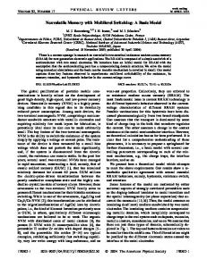
Fig. 1. (a) Schematics of the suspended SiNW formation by Bosch etching. (b) SEM image and magnified views of the suspended SiNW on the bulk substrate. (c) Horizontal and vertical TEM images in the LG direction in the AAG junctionless transistor with the O/N/O gate dielectric. The width (WNW ) and length (LG ) of the SiNW channel are approximately 10 and 50 nm, respectively. Thickness of the O/N/O layers for the charge storage node is 2.8 nm/6.2 nm/7 nm.
transistor to ensure high driving current and good S/D contact resistance. After patterning the active region with WNW = 30 nm, the Bosch process enabled by the RIE system was employed to form the suspended SiNW separated from the bulk substrate, as shown in Fig. 1(a). The suspended SiNW via the Bosch process is achieved by balancing anisotropic etching and passivation steps. Details of the Bosch process can be found in the literature [15]. The scanning electron microscopy (SEM) images in Fig. 1(b) clearly show the suspended SiNWs. The gap distance between the SiNW and bulk substrate is approximately 250 nm. After the formation of the SiNWs, channel stop implantation with boron ions is applied. Subsequently, sacrificial oxidation is employed to further reduce the width (WNW = 10 nm) of the SiNW and to make the channel smooth, followed by the formation of shallow trench isolation. Next, an O/N/O layer with a thickness of 2.8 nm/6.2 nm/7 nm (using the thermal oxide and the LP-CVD nitride/TEOS oxide) and an in situ n+ poly-Si gate (using the LP-CVD poly-Si) are formed sequentially. Afterward, a length (LG ) of 50 nm is patterned. Horizontal and vertical transmission electron microscopy (TEM) images of the fabricated junctionless transistor are shown in Fig. 1(c). III. R ESULTS AND D ISCUSSION Fig. 2(a) and (b) shows the typical transfer and output characteristics of the fabricated AAG junctionless transistor with the O/N/O gate dielectric, respectively. The transfer characteristics show good dc performance levels with an on/off ratio that exceeds 105 and good gate controllability even with an EOT of 13 nm. The subthreshold swing (SS) of the AAG junctionless
Fig. 3. P/E characteristics of the AAG junctionless transistor memory cell (LG = 50 nm and WNW = 10 nm). The P/E pulse is applied to the gate while maintaining the S/D at the ground potential for FN tunneling.
transistor is approximately 130 mV/dec. The relatively low threshold voltage (VT = −1.9 V at ID = 100 nA) is primarily due to the nature of the junctionless transistor, as we alternatively used n+ poly-Si rather than p+ poly-Si as a gate electrode. Moreover, thick gate dielectric layers can cause a more negative VT value compared to the VT value reported in the literature [12]. Additionally, the transconductance (gm ) at VD = 0.05 V, as shown in Fig. 1(a), reveals the typical property of the junctionless transistor. The electric field from the gate should be required to attract the inversion (accumulation) carriers in a nominal inversion (accumulation)-mode transistor. The junctionless transistor, on the other hand, is basically and normally turned on; thus, the ON-state current (ION ) is determined primarily by the doping concentration of the channel. Therefore, there is a zero electric field perpendicular to the current flow direction in the ON state. As a result, the gm value does not rapidly decrease as a result of the lower electric field in the SiNW channel. This indicates that the junctionless transistor inherits the scaling advantages. The AAG junctionless transistors with the O/N/O gate dielectric were characterized for program/erase (P/E) operations using the Fowler–Nordheim (FN) tunneling mechanism. For programming, positive pulses with magnitudes ranging from 11 to 14 V were applied to the gate while keeping the S/D grounded. For erasing, the cells were first programmed using a +14-V pulse for 1 ms, followed by negative pulses with magnitudes ranging from −12 to −15 V applied to the gate. Fig. 3 shows the typical P/E characteristics of the AAG junctionless transistor memory cell. A large programming window (ΔVT ) of up to 5 V is obtained without degradation of the SS (data are not shown). This can ensure multilevel operation for increased
604
IEEE ELECTRON DEVICE LETTERS, VOL. 32, NO. 5, MAY 2011
Fig. 4. (a) 105 -cycle endurance of the AAG junctionless transistor with the O/N/O gate dielectric. A program operation at +14 V for 100 μs and an erase operation at −14 V for 1 ms are used in the endurance test. (b) Retention characteristics for various postcycled samples at room temperature.
memory density. Due to the nature of the AAG structure, significantly erased saturation of the cells is not noted, even at −15 V, despite the n+ poly-Si gate. The P/E cycling endurance and postcycling retention characteristics of the junctionless transistor memory cell are shown in Fig. 4. The SS in the inset in Fig. 4(a) stays intact before 103 cycling, indicating slight damage during P (VG = 14 V for 100 μs)/E (VG = −14 V for 1 ms) cycling. Although the SS degradation is significant after 104 cycling due to the generation of the interface state, the P/E window does not narrow even after 105 cycles. Therefore, a data state can be sustained for such iterative cycling. In Fig. 4(b), the retention characteristics after each program (VG = 14 V for 100 μs) and erase (VG = −14 V for 1 ms) operation are investigated according to the number of P/E cycles. For the 105 cycling case, 47% of the original P/E window value is maintained for 2 × 10⁵ s. It is speculated that the amount of loss is caused by the tunneling oxide damage during the P/E cycling process. Moreover, this is attributed to the slight thin tunneling oxide. However, it is believed that, with proper engineering of the gate stack, e.g., bandgap engineering SONOS, the retention characteristics can be improved significantly. IV. C ONCLUSION A novel AAG junctionless transistor SONOS memory cell with acceptable P/E behaviors, cycling endurance, data retention, and dc performance has been demonstrated on a bulk substrate by utilizing a deep RIE system for the first time. The AAG junctionless transistor memory cell inherited the scaling advantages of not only the AAG structure but also the junctionless transistor. Therefore, the junctionless transistor memory cell is an excellent candidate for the next-generation 3-D NAND Flash memory below the 20-nm node. R EFERENCES [1] R. Liu, H.-T. Lue, K. C. Chen, and C.-Y. Lu, “Reliability of barrier engineered charge trapping devices for sub-30 nm NAND Flash,” in IEDM Tech. Dig., 2009, pp. 745–748. [2] K. Kim, “Technology for sub-50 nm DRAM and NAND Flash manufacturing,” in IEDM Tech. Dig., 2005, pp. 323–326. [3] H.-T. Lue, E.-K. Lai, Y. H. Hsiao, S. P. Hong, M. T. Wu, F. H. Hsu, N. Z. Lien, S. Y. Wang, L. W. Yang, T. Yang, K. C. Chen, K. Y. Hsieh, R. Liu, and C.-Y. Lu, “A novel junction-free BE-SONOS NAND Flash,” in VLSI Symp. Tech. Dig., 2008, pp. 140–141.
[4] H. Tanaka, M. Kido, K. Yahashi, M. Oomura, R. Katsumata, M. Kito, Y. Fukuzumi, M. Sato, Y. Nagata, Y. Matsuoka, Y. Iwata, H. Aochi, and A. Nitayama, “Bit cost scalable technology with punch and plug process for ultra high density Flash memory,” in VLSI Symp. Tech. Dig., 2007, pp. 14–15. [5] Y. Fukuzumi, R. Katsumata, M. Kito, M. Kido, M. Sato, H. Tanaka, Y. Nagata, Y. Matsuoka, Y. Iwata, H. Aochi, and A. Nitayama, “Optimal integration and characteristics of vertical array devices for ultra-high density, bit-cost scalable Flash memory,” in IEDM Tech. Dig., Dec. 2007, pp. 449–452. [6] Y. Komori, M. Kido, M. Kito, R. Katsumata, Y. Fukuzumi, H. Tanaka, Y. Nagata, M. Ishiduki, H. Aochi, and A. Nitayama, “Disturbless Flash memory due to high boost efficiency on BiCS structure and optimal memory film stack for ultra high density storage device,” in IEDM Tech. Dig., Dec. 2008, pp. 851–854. [7] J. Kim, A. J. Hong, S. M. Kim, E. B. Song, J. H. Park, J. Han, S. Choi, D. Jang, J.-T. Moon, and K. L. Wang, “Novel vertical-stacked-arraytransistor (VSAT) for ultra-high-density and cost-effective NAND Flash memory devices and SSD (solid state drive),” in VLSI Symp. Tech. Dig., 2009, pp. 186–187. [8] J. Jang, H.-S. Kim, W. Cho, H. Cho, J. Kim, S. I. Shim, Y. Jang, J.-H. Jeong, B.-K. Son, D. W. Kim, K. Kim, J.-J. Shim, J. S. Lim, K.-H. Kim, S. Y. Yi, J.-Y. Lim, D. Chung, H.-C. Moon, S. Hwang, J.-W. Lee, Y.-H. Son, U-I. Chung, and W.-S. Lee, “Vertical cell array using TCAT (terabit cell array transistor) technology for ultra high density NAND Flash memory,” in VLSI Symp. Tech. Dig., 2009, pp. 192–193. [9] W. Kim, S. Choi, J. Sung, T. Lee, C. Park, H. Ko, J. Jung, I. Yoo, and Y. Park, “Multi-layered vertical gate NAND Flash overcoming stacking limit for terabit density storage,” in VLSI Symp. Tech. Dig., 2009, pp. 188–189. [10] A. Hubert, E. Nowak, K. Tachi, V. Maffini-Alvaro, C. Vizioz, C. Arvet, J.-P. Colonna, J.-M. Hartmann, V. Loup, L. Baud, S. Pauliac, V. Delaye, C. Cara-basse, G. Molas, G. Ghibaudo, B. De Salvo, O. Faynot, and T. Ernst, “A stacked SONOS technology, up to 4 levels and 6 nm crystalline nanowires, with gate-all-around or independent gates (Φ-Flash), suitable for full 3-D integration,” in IEDM Tech. Dig., Dec. 2009, pp. 637–640. [11] A. J. Walker, “Sub-50-nm dual-gate thin-film transistors for monolithic 3-D Flash,” IEEE Trans. Electron Devices, vol. 56, no. 11, pp. 2703–2710, Nov. 2009. [12] J.-P. Colinge, C.-W. Lee, A. Afzalian, N. D. Akhavan, R. Yan, I. Ferain, P. Razavi, B. O’Neill, A. Blake, M. White, A.-M. Kelleher, B. McCarthy, and R. Murphy, “Nanowire transistors without junctions,” Nat. Nanotechnol., vol. 5, no. 3, pp. 225–229, Mar. 2010. [13] C.-W. Lee, A. Afzalian, N. D. Akhavan, R. Yan, I. Ferain, and J.-P. Colinge, “Junctionless multigate field-effect transistor,” Appl. Phys. Lett., vol. 94, no. 5, p. 053 511, Feb. 2009. [14] J.-P. Colinge, C.-W. Lee, I. Ferain, N. D. Akhavan, R. Yan, P. Razavi, R. Yu, A. N. Nazarov, and R. T. Doriac, “Reduced electric field in junctionless transistors,” Appl. Phys. Lett., vol. 96, no. 7, p. 073510, Feb. 2010. [15] R. M. Y. Ng, T. Wang, F. Liu, X. Zuo, J. He, and M. Chan, “Vertically stacked silicon nanowire transistors fabricated by inductive plasma etching and stress-limited oxidation,” IEEE Electron Device Lett., vol. 30, no. 5, pp. 520–522, May 2009.