Performance Optimization of an FPGA-Based Configurable Multiprocessor for Matrix Operations* Xiaofang Wang, Student Member and Sotirios G. Ziavras, Senior Member, IEEE Department of Electrical and Computer Engineering New Jersey Institute of Technology Newark, NJ 07102, USA
[email protected] Abstract Several driving forces have recently brought about significant advances in the field of configurable computing. They have also enabled parallel processing within a single field-programmable gate array (FPGA) chip. The ever-increasing complexity of application algorithms and the supercomputing crisis have made this new parallel-processing approach more important and pertinent. Its cost-effectiveness provides system designers with the greatest flexibility while imposing many challenges to current hardware and software codesign methodologies. This paper explores practical hardware and software design and implementation issues for FPGA-based configurable multiprocessors, based on the authors' first-hand experience with a shared-memory implementation of parallel LU factorization for sparse block-diagonal-bordered (BDB) matrices. We also propose a new dynamic load balancing strategy for parallel LU factorization on our system. Performance results are included to prove the viability of this new multiprocessor design approach.
1. Introduction The computation complexity of many application algorithms increases at a higher rate than Moore's Law [2]. The von Neumann architectural paradigm for microprocessors, which struggle to follow Moore's Law, is not obviously the solution to bridging this computing gap [1]. Meanwhile, the supercomputer market has shrunk in recent years after more than 20 years' efforts and tremendous investments. The demand for higher performance makes it necessary to build applicationspecific parallel architectures. At the same time, FPGA-based configurable
_______________________________ * This work was supported in part by the U. S. Department of Energy under grant ER63384.
computing is becoming more and more appealing and has resulted in impressive achievements for many computation-intensive applications [3, 5]. Recently available multi-million platform FPGAs with richer embedded feature sets, such as plenty of on-chip memory, DSP blocks and embedded hardware microprocessor IP cores, have made it feasible to build parallel systems on a programmable chip (PSOPC). [6] presents a recent example. We implemented a scalable shared-memory multiprocessor and mapped a parallel LU factorization algorithm onto an FPGA [7]. With its good performance, our machine shows the great potential of FPGA-based configurable technology for implementing parallel systems. Many relevant issues must still be addressed in this area. Moreover, as we all know from our experience with fixed parallel-computing architectures, the performance and efficiency of algorithms highly depend on a good match of the algorithm with the target hardware architecture. With FPGA-based platforms, we can adapt the architecture to match the communication and computation demands of the application. This new field demands better design methodologies to fully explore the hardware potential and achieve maximum system performance. This paper focuses on hardware/software codesign perspectives and presents the techniques that we have applied to optimize the performance of our FPGA-based configurable multiprocessor system for LU factorization. In order to further increase system efficiency, we propose a new dynamic scheduling algorithm that was tested with IEEE electric power 57-, 118- and 300-bus matrices using up to five-processor systems embedded into the Altera SOPC (System-On-a-ProgrammableChip) development board.
2.FPGA-Based Configurable Multiprocessors
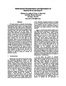
The new FPGA-based computing platforms present great challenges to current hardware-software codesign methodologies that are often based on a given CPUASIC hardware model [4]. Since the latter methodologies do not provide much choice to the hardware infrastructure, most of the efforts in optimizing the performance focus on the software. The boundary between hardware and software is decided upon before the separate software and hardware design teams begin their work using different languages, often C/C++ (and/or assembly code primarily for the critical part) and HDL, respectively. In contrast, new FPGA-based configurable computing strategies provide the system designer with several dimensions to optimize the design for application-specific performance. Full control is viable over most of the resources and enormous opportunities appear during the overall design process. We illustrate our new hardware-software codesign techniques that first optimize the algorithm and then analyze the application's communication-computation model for further optimization. Figure 1 shows our processor-based system model for the parallel BDB LU factorization algorithm [7]. The binary tree interconnection network matches well the data communication model in our algorithm. The processor-based approach that makes the PEs more localized than a large across-the-chip computing strategy is more preferable to modern SOPC designs. As the feature size of silicon processes enters the submicron range, the wire delay becomes even more significant compared to the logic delay, and it can even dominate the system's performance due to the reverse scaling of wires compared to transistors. Our binary tree network reduces dramatically global communications. By using configurable RISC processor IP cores, we add another dimension of programmability and flexibility to the FPGA-based computing engines. We can tailor the processor to the specific requirements of the application and include only those features that are needed by the latter. We can identify the critical instructions in the application code that affect performance the most and implement them as hardware logic. Table 1 shows the big difference of software (SW FP) and hardware floating-point (HW FP) operations for LU factorization on a variety of matrices. The configurable processor cores also provide us with more flexibility to integrate them in an SOPC environment with other IPs, compared to fixed processor cores.
3. Hardware Design and Implementation Issues The PE lies in the core of any computing machine. When using configurable processors, we need to carry out trade-offs between the processing power and the
resources being used. The processor datapath width, register file size, API functions, peripherals, data and Table 1. Comparison of software and hardware floating-point operations for LU factorization (in clock cycles) on the Altera Nios board Matrix Size 24 x 24 36 x 36 64 x 64 96 x 96 102 x 102
SW FP 3,328,615 11,489,708 70,502,845 228,013,002 274,946,133
HW FP 203,567 634,137 3,326,162 10,935,456 13,076,173
Speedup 16.35 18.12 21.20 20.85 21.03
instruction cache sizes, support for interrupts, resource utilization, embedded on-chip debugging capability, and hardware support for complex arithmetic functions should all be tailored to the specific requirements of the applications. We used a 32-bit Nios processor from Altera as the PE. The system controller is also implemented with Nios. The Nios RISC processor is a fully configurable soft processor running over 125 MHz in the Altera Stratix FPGA. The processor utilizes a 5stage pipeline and conforms to a modified Harvard memory architecture. A typical Nios processor in our machine consumes about 1700 logic elements in a Stratix FPGA. The number of PEs in our computing model is scalable, as shown in Figure 1. The operation of every PE is guided by the system controller (SC) that utilizes the boot code in the boot memory of every PE and the interrupt connection between every PE and this controller. The control channel is a star connection between the SC and every PE. There is also a direct communication channel between the controller and every PE through the dual-port on-chip memory. IC
DC
PE
SM To SC BOOT IM DM
SC: System Controller IC: Instruction Cache IM: Instruction Memory SM: Shared Memory
AVALONSCFABRIC
PE: Processing Element DC: Data Cache DM: Data Memory BOOT: Boot memory
Figure 1. Our multiprocessor architecture model
The memory hierarchy design and management are always major design issues for all computer systems. There have been many advanced memory management techniques for conventional microprocessors; they are directly supported by the operating systems and compilers. Due to the current lack of relevant software support in configurable machines, the memory design becomes a dominant factor in system performance. Moreover, while new silicon technology and computer architecture research facilitate faster processors, the performance gap between processors and memories tends to become larger. In our shared memory multiprocessor, the overall speedups may be quickly diminished due to severe memory contention and large system synchronization, if we rely solely on the on-board SRAM memory as the main runtime memory. Fortunately, new generation FPGAs make available more on-chip memory with wide communication channels. Our FPGA-based multiprocessor architecture capitalizes on this advantage and forms several kinds of memories in order to maximize performance. For example, we implemented a controller to manipulate the system's operation and pre-fetch instructions from the main memory into the PEs; the latter use the on-chip memory to run the application code because of its much lower access latency compared to the on-board SRAM memories. Table 2 summarizes the memory hierarchy and related characteristics. Table 2. Multiprocessor memory hierarchy Instruction Cache Data Cache Boot ROM Shared RAM Program Memory Data Memory
Configuration OC*, Single-port OC, Single-port OC, Single-port OC, Dual-port OC, Dual-port On-Board SSRAM OC, Dual-port
Capacity 4KB 4KB 2KB 2KB 12KB 256KB 8KB
Access master(s) Local PE Local PE Local PE Two neighbor PEs Local PE and SC SC Local PE and SC
*OC: On-Chip
The bootup program in the Boot ROM is implemented in assembly code and has size less than 2KB; it is used to communicate with the SC. The Shared RAM between two neighbors speeds up the system performance by eliminating the transfer of large blocks of data between memories. The sizes of the Shared RAM and Data Memory are determined based on the size of the largest 3-block matrix group that may appear in our algorithm [7] and the total available on-chip memory. We assign just enough space to the Boot ROM, Data Memory and Shared RAM in order to leave as much space as possible for the Program Memory. All the required interconnection between on-chip memories and/or processors is implemented based on a multi-
mastering, fully connected Avalon bus. Thus, the communication bandwidth is quite large and the on-chip memory access time is only one clock cycle. The cache can become a dominant architecture feature in the total execution time. For a given fixed processor, we focus on the efficient utilization of a cache of fixed size and configuration. For a configurable processor, we have choices in both hardware configuration and software optimization. Because it takes on the average at least 4 clock cycles to access the on-board synchronous SRAM memory, on-chip data and instruction caches are employed to reduce the memory access latency. In order to find an optimal size for our application, we compared the performance of a single processor with different instruction and cache sizes for the LU factorization algorithm applied to a 30 x 30 matrix. Our test results show that the cache configuration can make a difference of more than 20% in performance. Our multiprocessor targets complex matrix algorithms that require floating-point arithmetic to deal with dynamic data of wide range and some trigonometric functions, which take considerable time if implemented in software. We implemented the floating-point arithmetic and these functions in hardware, and interfaced the application code as custom instructions [7]. Such hardware customization also releases many resources to the processor for other tasks. We implemented serial and TCP connections between the multiprocessor and the host computer. The TCP network connection provides a flexible, quick and efficient communication channel for our FPGA-based parallel system, which can be accessed by all other hosts in the network. We may use the TCP port of the processor to send application code or reconfigure the system in its entirety, or in part, at runtime.
4. Mapping Applications to the Multiprocessor One of the most challenging tasks in programming parallel systems is load balancing. Our target application, i.e. parallel LU factorization of sparse matrices, is one of the hardest problems for dynamic load balancing due to its large amount of data dependences and occurrences of fill-ins (that is, zero elements become non-zero elements during factorization). Since our system does not currently have operating system support, we built a dedicated system controller to take care of load balancing at runtime; in this approach, all processors must report their load information to the controller. Let us begin with the preprocessing phase where we attempt to order the matrix into an optimal BDB matrix [7]. The best ordering is the one that keeps the 3-block groups as dense as possible while not making the last block too large. This way we can reduce the number of floating-point operations in the procedure that follows.
The best solution also depends on the detailed characteristics of the application matrix. Dynamic load balancing is carried out by the SC. The information that the host computer passes to the SC includes at least the size of the whole matrix, the number of the diagonal blocks, the size of every block and its memory addresses in the on-board memory. The SC always assigns the biggest available 3-block groups in the task queue. During the system configuration phase, the SC assigns the initial loads based on the information sent by the host computer. All the computing processors wait for the system information. Then, the SC copies the instructions and data stored in the on-board SSRAM into the local memories of all processors until they are filled up to the preset size. Then, every processor begins its work using its local data. If the next instruction is not in the local RAM, the processor generates a hardware interrupt to the SC and sends its status to the SC through the dual-port RAM. After receiving the interrupt, the SC checks the status of the corresponding processor, puts the interrupt in a queue, and continues processing the interrupts from this queue according to the FIFO priority. The SC keeps a load record for every processor in order to manage the unfinished jobs dynamically. The record entries include: the starting time of the working matrix group, the expected end time, the size of the working group, the possible next group for this processor, the phase the algorithm is in (that is, factorization or multiplication phase [7]), finished groups, etc. If one processor is idle (maybe because there is no work available or for some other reason), the SC first checks the status of the processors along the summation tree to find the nearest busy processor. It further decides whether it is worth asking the idle processor to help the working processor. The decision is based on the size of the working group, how much work has already been done (i.e., the used time divided by the expected time), and the current phase. During factorization, the idle processor will multiply the border blocks following the factorization of the working processor. If the working processor is in the multiplication phase and more than 1/3-rd of the work has not been done yet (this number is based on the computation/communication time ratio in our machine), then the SC will copy half of the remaining data to the idle processor and modify the working processor's load information. The multiplication results will be collected along the binary tree. Otherwise, the SC will look for another busy processor and will apply this check procedure again. We tested our parallel BDB LU factorization with this dynamic scheduling policy for the IEEE electric power 56-, 118- and 300-bus test matrices for up to 5-processor systems in the Altera SOPC development board. The performance comparison of the static and dynamic load balancing techniques for
different numbers of PEs is shown in Table 3. Generally, the larger the input matrix, the better the performance of dynamic scheduling. Table 3. Speedups (over uni-processor) with static and dynamic load balancing for the IEEE test matrices Number of PEs 57-bus D* 118-bus 300-bus 57-bus S* 118-bus 300-bus S: Static Scheduling
2 1.90 1.94 1.96 1.90 1.94
3 2.66 2.72 2.74 2.81 2.81
4 3.40 3.48 3.67 3.40 3.48
5 3.61 4.21 4.16 4.05 4.36
1.96 2.83 3.67 D: Dynamic Scheduling
4.37
5. Conclusions We have presented our hardware and software design effort for a shared-memory multiprocessor implemented within an FPGA. This computing paradigm provides tremendous opportunities along several dimensions: system, hardware, and software. Due to the lack of hardware-software codesign platforms, this procedure requires that the designer be proficient in algorithms, system-level design, software/hardware partitioning, architecture design, and software/hardware coding. Our multiprocessor targets LU factorization. Our proposed dynamic load balancing algorithm for this machine yields good performance and highlights our observation about the need for hardware-software codesign efforts.
References [1]. R. Hartenstein, “The Microprocessor is no more General Purpose: Why Future Reconfigurable Platforms Will Win,” invited paper, Proc. of the Int'l Conf. on Innovative Syst. in Silicon (ISIS’97), Austin, Texas, Oct. 1997. [2]. K. Sarrigeorgidis and J. M. Rabaey, "Massively Parallel Wireless Reconfigurable Processor Architecture and Programming," 10th Reconfigurable Architectures Workshop (RAW 2003), Nice, France, April 2003. [3]. R. Hartenstein, "Are We ready for the Breakthrough?" keynote address, 10th Reconfigurable Architectures Workshop 2003 (RAW 2003), Nice, France, April 2003. [4]. W. Wolf, “A Decade of Hardware/Software Codesign,” IEEE Computer, Vol.2, pp. 801 –808. [5]. K. Compton and S. Hauck, “Reconfigurable Computing: A Survey of Systems and Software,” ACM Comput. Surveys, Vol. 34, No. 2., June 2002, pp. 171-210. [6]. C. Wolinski, M. Gokhale, and K. McCabe, "A Polymorphous Computing Fabtric," IEEE Micro, Vol. 22, No. 5, Sep/Oct. 2002, pp. 56-68. [7]. X. Wang and S.G. Ziavras, "Parallel LU Factorization of Sparse Matrices on FPGA-Based Configurable Computing Engines," Concurrency and Computation: Practice and Experience, accepted for publication, Jan. 2003.