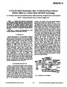
Abstract- In this article, the mathematical analysis is proposed to describe phase noise phenomenon. The principle of this proposed scheme is based on the ...
Phase noise phenomenon explanation based multi-time variables differential equation technique Kunanon Kittipute* Panwit Tuwanut and Paramote Wardkein* Faculty of Information Technology Telecommunication Engineering Department, Faculty of Engineering*, King Mongkut’s Institute of Technology Ladkrabang Ladkrabang, Bangkok, THAILAND 10520 Abstract- In this article, the mathematical analysis is proposed to describe phase noise phenomenon. The principle of this proposed scheme is based on the multitime variables differential equation technique. The analytic result clearly shows that noise is composed of multiplicative noise that spread around an oscillated frequency and additive noise acts as a noise floor of a system. To verify the proposed analysis, the computer simulation results are given which demonstrate that the obtained results agree well with the theoretical counterpart. I.
INTRODUCTION
In communication system, sinusoidal oscillator is widely used, especially for generating a carrier signal in a modulator and a demodulator circuit. In ideal case, the spectrum of an ideal ωc sinusoidal signal is a single line located at the frequency ωc as depicted in Fig 1(a). But for real sinusoidal signal, its spectrum located at frequency ωc is shape-liked a skirt as shown in Fig 1(b). The double-sided spectra which spread around the center frequency ωc are known as phase noise. This phase noise has an affect on a transmitter and a receiver in a communication system as illustrated in Fig. 2 and Fig. 3, respectively. In a transmitter, it causes the spectra of an information signal which occur around a carrier signal be covered with this phase noise as shown in Fig. 2. In the North America Digital Cellular IS54 standard, the power per unit bandwidth of phase noise must be below the power of a carrier signal at an offset frequency ( Δω ) of 60 kHz about 115dB (-115dBc/Hz) [1]. At a receiver, the phase noise occurred at a local oscillator will also present in down converted frequency signal as shown in Fig. 3. Due to this problem, many researchers [1-3] have been attempted to describe the phase noise phenomenon. But mostly, phase noise is said to be caused by nonlinearity in nature of a system or devices. To describe such phenomenon, a novel scheme based on multi-time differential equation technique is proposed in this paper. The proposed mathematic analysis provides clearly explanation that how phase-noise is happened. The outline of this paper will be arranged as follows. In section II, the principles are discussed where the simulation
results are provided in section III. Finally the conclusion is given in section IV. II. PRINCIPLES A. Noise sources Noise sources can be classified into two broad classes of sources; those external to the system such as atmospheric, solar, or man-made sources, and those internal to the system. The effect of the external noise sources on the system is difficult to be analyzed, depending heavily upon system location and configuration [4]. The main consideration of the analysis and design of communication systems is thus relative to the internal noise sources. There are many mechanisms related to the internal noise, some of them will be briefly discussed. Firstly, thermal noise or Johnson noise is generated
(a)
Figure 1. Frequency spectrum of an ideal sinusoidal signal, (b) a real sinusoidal signal.
Figure 2. The effect of phase noise in a transmitter.
Figure 3. The effect of phase noise in a receiver.
978-1-4673-9749-0/16/$31.00 ©2016 IEEE
by the thermal motion of electron in a resistor that is directly proportional to the temperature. The mean-square thermal noise voltage appearing across a resistor R ohms at temperature T Kelvin is vn2 = 4kTRΔf .
(1)
where k is the Boltzmann’s constant ( 1.38 × 10 −23 J/K ) and Δf is the bandwidth in Hertz. Next, as current is carried by discrete charge, electrons, the current flow is not continuous. Thus, the current which appear to be a steady current, it, in fact, is composed of a large number of random independent current pulses. This gives rise to shot noise whenever current flows. Shot noise is most easily seen in semiconductor devices, i.e. diodes, transistor and MOS. It can be shown that if a current I is composed of a series of independent pulses with average value I DC , then the noise current has mean-square value of in2 = 2qI DC Δf
α I DC Δf fβ
(3)
about unity, I DC is a direct current , K is a variable depending on a device process and Δf is the bandwidth in Hertz. A typical combination of white noise and flicker noise is depicted in Fig. 4 where the corner frequency is usually defined by the flicker noise.
B. Sinusoidal oscillator and phase noise For a sinusoidal oscillator, it can be modeled as a second or higher order differential equation [5,6]. For simplicity of explanation, let us consider the second order differential equation as a mathematical model of the oscillator, which is dt 2
+ a1
dy ( t ) dt
+ a0 y ( t ) = 0
978-1-4673-9749-0/16/$31.00 ©2016 IEEE
a0 , a1 are known parameters and x ( t ) is the input
signal of the system. The total response y ( t ) of the system is
composed of natural response yn ( t ) and force response y f ( t ) then y ( t ) = yn ( t ) + y f ( t ) . For the natural response, it
is determined by
d 2 y (t ) dt
2
+ a1
dy ( t ) dt
+ a0 y ( t ) = 0 .
(5)
Hence,
yn ( t ) = C1e(σ + jω )t + C2 e(σ − jω )t
(6)
where C1 and C2 are constants which can be obtained by initial conditions at t = 0 , σ = − a1 / 2 is a damping factor , and ω is a natural frequency which is
a12 − 4a0 / 2 . Next,
the force response y f ( t ) can be solved as following
d 2 y f (t ) dt
2
+ a1
dy f ( t ) dt
+ a0 y f ( t ) = x ( t ) .
(7)
Then, the total response of the system can be expressed as
y ( t ) = C1e(σ + jω )t + C2 e(σ − jω )t + y f ( t ) .
(8)
To eliminate a damping effect, a1 is set to be zero whereas
C1 , C2 are set to be C / 2 , which results in
where α is a constant in range 0.5 to 2 , β is a constant
d 2 y (t )
where
(2)
where q is charge of the electron ( 1.6 × 10 −19 C ) and Δf is the bandwidth in Hertz. Thermal noise and shot noise are both white noise sources that the power spectrum density (PSD) is equal power in each frequency interval. In other words, the power per unit bandwidth is constant. In addition to thermal and shot noise, 1/ f noise or flicker noise also contributes to internally generated noise. This noise occurs in almost all electronic devices, and results from various causes, such as impurities in a conductive channel, generation and recombination noise in a transistor due to base current, and so on. It is always related to a direct current and it is a low-frequency phenomenon, as the high frequencies are overshadowed by the other noise sources. This noise takes the form of
in2 = K
Figure 4. Total noise spectra in a system.
(4)
y ( t ) = C cos (ω t ) + y f ( t ) .
(9)
As seen in (9), the output signal is composed of a sinusoidal signal and a force signal represents an input signal. To determine amplitude of the sinusoidal output, it can be achieved by substituting the initial conditions at t = 0 , which dy (0) are y ( 0 ) = A and = 0 , thus yields C = A − y f ( 0 ) . dt The total response therefore is
y ( t ) = ( A − y f ( 0 ) ) cos (ωt ) + y f ( t ) .
(10)
As result given by (10), it implies that amplitude of sinusoidal signal is constant even though the forcing input signal is timevarying. Recently, T. Maneechukate et al. [6] proposed a new analysis of a second-order system based on multi-time technique [7] and found that the amplitude of sinusoidal signal
is also varied according to the forcing input signal. To clarify phase noise phenomenon in this paper, the analysis of a second-order system based on multi-time variables technique is briefly reviewed It should be noted that another time variable τ is introduced. The second-order differential equation of the oscillator is thus given by d 2 y f (τ ) dτ
2
+ a1
dy f (τ ) dτ
+ a0 y f (τ ) = x (τ )
(11)
where the total response is rewritten to be y ( t ,τ ) = C cos (ω t ) + y f (τ ) .
(12)
In this case, the amplitude C is determined by substituting the initial conditions at t = 0 , which are y ( 0,τ ) = A and dy ( 0,τ ) dt
= 0 where C = A − y f (τ ) .
(13)
where VSAT is an initial condition voltage at t = 0 , y ( 0,τ ) = VSAT and
dy ( 0,τ )
= 0 . The natural frequency of this dt circuit is set at 3.15 MHz. Firstly, the phenomenon that the amplitude of sinusoidal signal is varied to the forced response is observed. The sinusoidal signal with amplitude 0.5Vpp, offset voltage 0.5V and frequency 100 kHz is employed to at t = 10 μ s . The simulation result is depicted in Fig. 7 and the output’s spectra are shown in Fig. 8. From Fig. 7, the amplitude of the oscillated output is first constant before the forcing input signal is fed. As can be seen after the forcing input signal is fed to the system, the amplitude of the output is varied to the forced response. Additionally, the spectra of the output shown in Fig. 8 are of the sinusoidal signal, of the forced response and of the multiplicative between the sinusoidal signal and the forced response.
The total response then is y ( t ,τ ) = A cos (ω t ) − y f (τ ) cos (ω t ) + y f (τ ) .
(14)
As can be seen in (14), the amplitude of sinusoidal oscillator depends on the initial conditions at t = 0 and the forced response at any arbitrary time. In addition, if the system has the noise voltage n (τ ) at the input node of the system, for
τ = t + t0 by initial time t0 ≈ 0 , then τ ≈ t , the output signal thus can be expressed as
Figure 5. Output’s spectrum of the system.
y ( t ) = A cos (ω t ) − n f ( t ) cos (ω t ) + n f ( t ) .
(15)
The first term of (15) is the sinusoidal signal, the second term is called a multiplicative noise and the last term is an additive noise. As the total noise spectra shown in Fig. 4, hence the output spectra of the system can be depicted in Fig. 5. It thus implies that the sinusoidal spectrum is not a single impulse, but be around with the total noise that acts as a multiplicative noise or phase noise, and the additive noise acts as a noise floor. III. SIMULATION RESULTS
Figure 6. The JFET Colpit oscillator.
The JFET Colpit oscillator as illustrated in Fig.6 is used to be a circuit for verification of the proposed principle. The system equation of the JFET Colpit oscillator is given by LC
d 2 v f (τ ) dτ 2
+ v f (τ ) = vi (τ )
(16)
where the total response with t0 ≈ 0 is
1 y ( t ) = (VSAT − v f ( t ) ) cos t + v f (t ) LC
(17)
Figure 7. The upper trace is the input signal that fed at t = 10μ s . The lower trace is the output signal of the system.
simulation results have been demonstrated which agree well with the theoretical anticipation.
Figure 9. The upper trace is the input noise spectra. The Lower trace is the output noise spectra. Figure 8. The spectra of the output signal.
Moreover, the total noise is employed to be an input of the JFET Colpit oscillator where expected output spectra are as given in Fig. 5. The results are demonstrated in Fig. 9 where the upper trace is the input noise spectra (representing the total noise) and the lower trace is the resulted output noise spectra. It is seen that the output noise spectra are composed of the sinusoidal spectrum which is around with the total noise (phase noise), and the additive noise floor. IV. CONCLUSIONS A novel mathematical analysis for phase noise phenomenon explanation is proposed in this work. The proposed mathematical scheme is based on the multi-time variables differential equation technique. The obtained analytical result is clearly indicated that the phase noise in the system is due to the multiplication between the noise response and the sinusoidal signal. It thus results in the spectrum of the sinusoidal frequency be covered with multiplicative noise. The
REFERENCES [1] [2] [3] [4] [5] [6]
[7]
Behzad Razavi, “A study of Phase noise in CMOS Oscillator,” IEEE Journal of solid-state circuit, vol. 30, March 1996, pp.331-343. D.B. Leeson, “A simple model of feedback oscillator noise spectrum,” Proc. IEEE, pp.329-330, Feb. 1966. A. A. Abidi and R. G. Meyer, “Noise in relaxation oscillators,” IEEE J. Solid-State Circuits, Vol. SC-18, Dec. 1983, pp. 794-802. R.E. Ziemer and W.H. Tranter, Principles of Communications, 5th ed., John Wiley & Sons Inc., 2002, pp.579-583. R. Punchalard, J. Koseeyaporn, and P. Wardkein, “Analytic Solution of Amplitude Controlled Digital Oscillator Using Multi-Time Variables Technique,” IEEE APCCAS 2006, 4-7 Dec. 2006, pp.2012 – 2015. T. Maneechukate, P. Tuwanut, J. Koseeyapom, and P. Wardkein, “New analytic solution of second-order oscillator using multi-time variables technique,” IEEE Int. Symp. Intelligent Signal Processing and Communication Systems, Dec. 2005, pp.637-640. J. Roychowdhury, “Analyzing circuits with widely separated time scales using numerical PDE methods,” IEEE Trans. Circuits and Systems Fundamental Theory and Application, vol. 48, 5, 2001, pp. 578-594.