comprising of multiplexers, current mirrors, high compliance current sinks and ... silicon technology and advances our research on POSFET tactile sensing [9, 10, ...
Pre-print article. Please use following data for citations/reference – Dahiya, R.S.; Adami, A.; Collini, C.; Valle, M.; Lorenzelli, L., "POSFET tactile sensing chips using CMOS technology," 2013 IEEE Sensors, vol., no., pp.1,4, 3-6 Nov. 2013; doi: 10.1109/ICSENS.2013.6688149
POSFET Tactile Sensing Chips Using CMOS Technology Ravinder S. Dahiya1, Andrea Adami2, Cristian Collini2, Maurizio Valle3, Leandro Lorenzelli2 1
Electronics and Nanoscale Engineering Research Division, University of Glasgow, G12 8QQ, UK, Bio-MEMS, Centre for Materials and Microsystems, Fondazione Bruno Kessler, Trento, 38123, Italy, 3 DITEN, University of Genoa, 16145, Italy
2
Abstract—This work presents the advanced version of novel POSFET (Piezoelectric Oxide Semiconductor Field Effect Transistor) devices based tactile sensing chip. The tactile sensing chip in the new version, presented here, has been fabricated using CMOS (Complementary Metal Oxide Semiconductor) technology. The chip consists of 4 x 4 POSFET touch sensing devices, four temperature diodes, and the electronic circuitry comprising of multiplexers, current mirrors, high compliance current sinks and voltage output buffers. The on chip POSFET devices have linear response in the tested dynamic contact forces range of 0.01–3N and the sensitivity (without amplification) is 102.4 mV/N.
I.
INTRODUCTION
Touch sensing plays an important role in various application domains such as robotics, electrotextiles and medical prosthesis. A large amount of efforts has been devoted on the development of tactile sensors and over the years many new touch sensors using different materials and transduction methods have been presented [1, 2]. The suitability of these sensors to above applications depends on a number of constraints including sensor size, sensor response time, and physical features such as bendability or conformability of the sensor patch etc. [3]. For instance, many times the sensors are big in size. Considering also the electronic circuitry associated with sensors the big sized sensors are unsuitable for body sites like robot’s fingertips, where large numbers of sensors with high density are needed. For this reason, MEMS based miniaturized touch sensors with on-chip electronics have been explored in past [4]. Similarly, mechanically flexibility has been achieved in touch sensing schemes by using Organic Field Effect Transistors (OFET), fibers, and flexible Printed Circuit Boards (PCB) for sensors have been reported recently for measuring parameters such as pressure, contact force and temperature [5-8]. Silicon technology has also been explored for miniaturized touch sensors [9-11]. With precision down to sub-micron scale and the high quality of materials the silicon technology offers avenues for developing high-performing and miniaturized sensors with possibility of accommodating the electronics on same chip - leading to a full on chip tactile sensing system. The tactile sensing system on chip will be a potent solution for reducing the number of wires, which is needed in application
such as robotic hands to improve dexterity. The touch sensing chip reported in this work explores this opportunity offered by silicon technology and advances our research on POSFET tactile sensing [9, 10, 12, 13], by realizing on the same chip a 4 x 4 array of POSFET devices, four temperature diodes and the basic electronics comprising of multiplexers, current mirrors, high compliance current sinks and voltage output buffers. The chip has been fabricated using CMOS technology. The design, fabrication and evaluation of the advanced version of POSFET tactile sensing chip are explained in the following sections. II.
CONECEPT OF A POSFET DEVICE
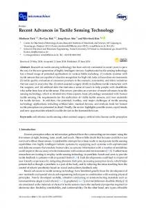
A POSFET touch sensing device has the structure similar to the one shown in Fig. 1. The POSFET devices are fabricated by spin coating piezoelectric polymer P(VDFTrFE) film on the gate area of MOS devices and polarizing the polymer film in situ. The piezoelectric polymer film is therefore an integral part of the device. The remnant polarization (Pr) of the polarized polymer results in an intrinsic electrical dipole equivalent to fixed charges ±Q, as shown in Fig. 1. In real devices, either through external connections or parasitic resistance of the capacitor, free charge is redistributed on capacitor terminal in order to compensate the electrical dipole. When external force is applied on the POSFET device, additional charges (which are proportional to the applied force) reflect into the channel, thereby modulating the induced channel. In this way the (contact) force is directly reflected as the variation in channel current of the POSFET devices – which can be further processed by on-chip electronic circuitry such as the one presented in this work. Similar approaches, but using extended gates, have been reported in the past for pressure and touch sensing [11, 14, 15]. In the extended gate approach, the gate terminal of a MOS device is connected to a large size electrode or to an extended gate that is located elsewhere on the chip. Like POSFETs, the extended gate approach too brings the sensor and conditioning electronics closer and hence the overall response is better than the conventional approach – where the sensor and conditioning electronics are placed apart. However, extended gates introduce a large substrate capacitance (whose value depends on the substrate), which in turn, significantly
Pre-print article. Please use following data for citations/reference – Dahiya, R.S.; Adami, A.; Collini, C.; Valle, M.; Lorenzelli, L., "POSFET tactile sensing chips using CMOS technology," 2013 IEEE Sensors, vol., no., pp.1,4, 3-6 Nov. 2013; doi: 10.1109/ICSENS.2013.6688149
Fig. 1: The working of POSFET touch sensing device. attenuates the voltage available at the gate terminals of MOS transistors. Thus, benefits of closely located sensor and electronics are not fully exploited with extended gate approach. With piezoelectric polymer on the gate of the MOS itself, the POSFET touch sensing devices are relatively free from such issues. Further, unlike extended gate approach, the POSFETs occupy smaller area on the chip. The saved silicon area can be used to accommodate on-chip electronics and signal conditioning/processing circuitry, as done in this work. III.
DESIGN OF TACTILE SENSING CHIP COMPONENTS
The tactile sensing chip (Fig 2) presented here consists of 4 x 4 POSFETs, four temperature diodes, and basic electronic circuitry comprising of multiplexers, current mirrors, high compliance current sink and output buffers. The design of these components is presented below. A. Design of POSFET devices The POSFET devices have been designed to have an active area of 0.9 mm x 0.6 mm, so as to obtain spatial acuity comparable to that of human fingertips (∼1 mm) [16]. The nMOSFET devices have been designed to have an aspect ratio (W/L) of about 273 for large transconductance (gm). The large value of channel width (W) is obtained by designing a serpentine like or interdigitated gate structure, as explained elsewhere [12, 13]. The length of source and drain diffusions have been modified in the new design from about 10 squares to 2. Considering typical sheet resistance of about 600 Ω/sq, the source/drain resistance in the new design is about 120 Ω/sq. The parasitic resistance is thus reduced by a factor 5 – which reflects a significant improvement of the actual transconductance over the previous device implementations [9, 10]. In operative conditions the transistor is used in source follower configuration, using either a pull-down resistor or a current sink with current mirrors connected to source, while the FET gate i.e. the lower electrode of the P(VDF–TrFE) piezoelectric film, is floating and the top contact is short-circuited to drain. The chosen source–follower configuration does not provide signal amplification like a common source configuration. Nonetheless, this configuration provides higher robustness to gain value mismatches between different devices, which is useful when an array of sensors is used, as in this work.
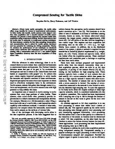
Fig. 2: (a) Image of the tactile sensing chip with on-chip electronics, fabricated using CMOS technology. (b) The scheme of tactile array and on-chip electronics. B. Design of POSFET Arrays The POSFET array comprises of 4 x 4 touch sensing devices to map the contact forces applied in the chip area. The overall size of the chip is 9 mm × 11 mm, with 1 mm center-tocenter pitch of sensor elements, which can be further scaled down. In order to reduce the number of interconnects and the contact pads, each row of the array shares the drain contact, as shown in Fig. 2a. The integrated array design allows us to implement a high density sensors array – which makes the POSFET tactile sensing chips suitable for applications such as manipulation and exploration of objects using robotic hands and fingers, where human like tactile spatiotemporal response is desired. C. Design of Temperature Diodes Four diodes implemented on the tactile sensing chip (Fig. 2a) provide the capability to measure contact temperature and the information related to variations in the chip temperature so as to allow for compensating the temperature variations related change in the response of POSFET devices. The diodes are realized with n+ regions implanted on p-well diffusions with 118 µm x 118 µm junction area. The diodes
Pre-print article. Please use following data for citations/reference – Dahiya, R.S.; Adami, A.; Collini, C.; Valle, M.; Lorenzelli, L., "POSFET tactile sensing chips using CMOS technology," 2013 IEEE Sensors, vol., no., pp.1,4, 3-6 Nov. 2013; doi: 10.1109/ICSENS.2013.6688149
are designed to work with 100 µA forward current in order to exploit the diode temperature coefficient. D. Design of Basic Electronics on the chip The basic electronic circuitry comprising of multiplexers, current mirrors, high compliance current sink and output buffers (Fig. 2b). The on-chip current sink bias the POSFETs in the common drain configuration. The supply voltage Vss has been set to -3.3V to be compliant with the external off-theshelf components. This value can be decreased effectively down to – 5V and lower. The bias sink circuit has been implemented by a simple current mirror. The details of highcompliance current sink are explained in [13]. To properly test the on-chip circuitry, the current is set externally to the chip. The current sink value Ibias has been set to 100 µA. In order to minimize POSFETs access and response time, the tactile sensing array has been arranged in two 4 x 2 sub-arrays (see Fig. 2b). Each sub-array is addressed independently from the other by 8 x 1 multiplexer. In order to minimize silicon area, each current sink is time-multiplexed among the POSFETs of the sub-array, i.e. only one POSFET at a time is addressed. The address circuitry (an analog CMOS multiplexer) is shown in Fig. 3. To decrease circuit complexity, the addressing 8 x 1 multiplexer has been implemented by a 4 input NAND gate with resistive pull up network (resistor R5 in Fig. 3); the NAND output is subsequently buffered by two inverters which generate the direct and negate signals to control one of the CMOS transfer gates of the analog
multiplexer. The propagation time of the analog multiplexer is in the order of 20 µsec. The timing has been organized in such a way that two POSFETs (one for each sub-array) can be addressed simultaneously: when a POSFET output is being accessed by the external circuitry, another one in the other sub-array is addressed is such a way that the transient time of the second POSFET will be elapsed when such POSFET will be accessed by the external circuitry as well. At that time, next POSFET in the former sub-array will be selected and so on. In this way, the switch-on POSFET transient time does not add to the POSFET address time. The POSFET voltage output is buffered by the two-stage buffer circuit shown in Fig. 4. The configuration uses a two stage common source amplifier with a feedback on active load of the first stage to set the closed loop gain near to unity. The buffer circuit has been implemented by only NMOS transistors to tackle with the availability of one metal layer in the given technology. The on-chip directly drives the output pad and decouples the POSFETs from the output of the chip. IV.
FABRICATION OF POSFET CHIP
The detailed CMOS fabrication process of the POSFET chips is explained elsewhere [12, 13]. In brief, the process is based on a non-standard 4-µm CMOS technology with Al gate and nMOS transistors on p-well. Process has been implemented on n-type wafers with resistivity 10 ÷ 12 Ωcm. The fabrication starts with boron implant and diffusion to create deep p-wells to insulate the n-type devices. Based on simulation and testing the p-well is 7.7 µm deep with sheet resistance 3 kΩ/sq. Implant of phosphorus and boron in p- and n-channel stop regions is performed in order to avoid shortcircuits between different structures. Then, after growing a 500 nm-thick field oxide, source and drain regions are defined and implanted using BF2 and double As/P doping for p-type and n-type respectively, with a resulting sheet resistance of about 60 Ω/sq. Gate region is opened and threshold adjustment is performed. A Si3N4/SiO2 double layer with equivalent thickness 45 nm is used as gate dielectric. The double layer dielectric is inherited from the template technology, originally developed for integrated chemical
Fig. 3: The scheme of the address circuitry.
Fig. 4: The scheme of the buffer circuit.
Fig. 5: The response of an on chip POSFET device with different normal forces and comparison with the previous POSFET device response.
Pre-print article. Please use following data for citations/reference – Dahiya, R.S.; Adami, A.; Collini, C.; Valle, M.; Lorenzelli, L., "POSFET tactile sensing chips using CMOS technology," 2013 IEEE Sensors, vol., no., pp.1,4, 3-6 Nov. 2013; doi: 10.1109/ICSENS.2013.6688149
sensors [17]. A single layer SiO2 gate dielectric would provide similar device properties. A 500 nm-thick layer of LPCVD LTO (Low Temperature Oxide) silicon oxide is deposited for electrical insulation, followed by contact hole realization and patterning of Al wires. Then, the FET section of the device is completed with the deposition of a second layer of 300 nm of LPCVD LTO to insulate Al wires, with openings for electrical contacts. Then, a 2.5 µm thick P(VDF-TrFE) piezoelectric film is spin coated on the wafer and top metal (Cr/Au) is then deposited by e-gun evaporation and further defined over the gate area of POSFET only. The metal is also used as mask during subsequent plasma etching of the polymer. The fabrication steps related to deposition and processing of piezoelectric polymer film are similar to those reported in [18]. V.
CONCLUSION
The development and testing of advanced version of tactile sensing chip having an array of 16 POSFET elements and basic on-chip electronics has been presented in this work. The improved POSFET design along with on-chip electronics result in a response that is more than twice that of the previous version. In future, the response of whole tactile sensing array will be evaluated. For applications such as robotics, integrated tactile system implemented with CMOS technologies can be of great advantage as this will allow the reduction of wiring complexity by implementing on-chip local data processing and multiplexing. Such approach will also make it easy to handle the large amount of tactile data. ACKNOWLEDGMENT This work was partly supported by the European Commission under grant agreements PCOFUND–GA–2008– 226070–Trentino, PITN–GA–2012–317488-CONTEST, and the Italian MIUR Project PRIN 2007 “Tactile Sensing System for Humanoid Robots Using Piezo-Polymer-FET Devices”.
R. S. Dahiya, P. Mittendorfer, M. Valle, G. Cheng, and V. Lumelsky, "Directions Towards Effective Utilization of Tactile Skin -- A Review," IEEE Sensors J., pp. 1--18, 2013 (in press).
[4]
H. Okada, M. Yawata, M. Ishida, K. Sawada, and H. Takao, "A membrane type Si-MEMS tactile imager with fingerprint structure for realization of slip sensing capability," in 23rd Int. Conf. on Micro Electro Mechanical Systems (MEMS), 2010, pp. 608-611.
[5]
P. Mittendorfer and G. Cheng, "Humanoid Multimodal Tactile-
[6]
S. C. B. Mannsfeld, B. C. K. Tee, R. M. Stoltenberg, C. V. H. H.
Sensing Modules," IEEE Trans. Rob., vol. 27, pp. 401-410, 2011. Chen, S. Barman, B. V. O. Muir, A. N. Sokolov, C. Reese, and Z. Bao, "Highly sensitive flexible pressure sensors with microstructured rubber dielectric layers," Nature Mater., vol. 9, pp. 859-864, 2010. [7]
G. Kita, Y. Suzuki, M. Shikida, and K. Sato, "Fabric tactile sensor composed of ball-shaped umbonal fibre for detecting normal and
RESULTS
The response of POSFET device was observed by applying a dynamic force (sinusoidal, 1–1000 Hz) in normal direction on the device, as per scheme given in [12]. The maximum voltage outputs of POSFET device for a normal dynamic force in the range 0.01–3 N are shown in Fig. 5. The plot is linear with sensitivity of POSFET devices equal to 102.4 mV/N, which is more than twice the value reported earlier [9]. The experimental conditions were similar to our previous works. The POSFET devices are capable of detecting contact forces as low as 0.01 N (∼1 gmf) [13], with negligible delay between input force and output of POSFET. VI.
[3]
lateral force," IET Micro & Nano Letters, vol. 5, pp. 211-214, 2010. [8]
G. Cannata, R. S. Dahiya, M. Maggiali, F. Mastrogiovanni, G. Metta, and M. Valle, "Modular skin for humanoid robot systems," presented at the 4th Int. Conf. on Cognitive Systems (CogSys), Zurich, 2010.
[9]
R. S. Dahiya, G. Metta, M. Valle, A. Adami, and L. Lorenzelli, "Piezoelectric oxide semiconductor field effect transistor touch sensing devices," App. Phys. Lett., vol. 95, pp. 034105(1-3), 2009.
[10] R. S. Dahiya, D. Cattin, A. Adami, C. Collini, L. Barboni, M. Valle, L. Lorenzelli, R. Oboe, G. Metta, and F. Brunetti, "Towards Tactile Sensing System on Chip for Robotic Applications," IEEE Sensors Journal, vol. 11, pp. 3216-3226, 2011. [11] E. S. Kolesar and C. S. Dyson, "Object Imaging with a Piezoelectric Robotic Tactile Sensor," Journal of Microelectromech. Sys., vol. 4, pp. 87-96, 1995. [12] R. S. Dahiya, A. Adami, C. Collini, and L. Lorenzelli, "POSFET Tactile Sensing Arrays using CMOS Technology," Sensors and Actuators - A, vol. doi:10.1016/j.sna.2013.02.007, 2013. [13] A. Adami, R. S. Dahiya, C. Collini, D. Cattin, and L. Lorenzelli, "POSFET touch sensor with CMOS integrated signal conditioning electronics," Sensors & Act.s A: Physical, vol. 98, pp. 502-507, 2012. [14] I. Graz, M. Kaltenbrunner, C. Keplinger, R. Schwodiauer, S. Bauer, S. P. Lacour, and S. Wagner, "Flexible ferroelectret field-effect transistor for large-area sensor skins and microphones," Appl. Phys. Lett., vol. 89, pp. 073501-3, 2006. [15] S. Decherchi, P. Gastaldo, R. S. Dahiya, M. Valle, R. Zunino, "Tactile-Data
Classification
of
Contact
Materials
Using
Computational Intelligence," IEEE Trans. Rob., vol. 27, pp. 635-639, 2011. [16] J. M. Wolfe, K. R. Kluender, D. M. Levi, L. M. Bartoshuk, R. S. Herz, R. L. Klatzky, and S. J. Lederman, Sensation and Perception. Sunderland, Massachusetts USA: Sinauer Associates Inc., 2006. [17] A. Adami, C. Ress, C. Collini, S. Pedrotti, L. Lorenzelli,
REFERENCES [1]
R. S. Dahiya and M. Valle, Robotic Tactile Sensing – Technologies and System (ISBN: 978-94-007-0578-4). Dordrecht: Springer Science + Business Media, 2013.
[2]
R. S. Dahiya, G. Metta, M. Valle, G. Sandini, "Tactile Sensing - From Humans to Humanoids," IEEE Trans Rob, vol. 26, pp. 1-20, 2010.
"Development of an integrated electrochemical system for in vitro yeast viability testing," Biosens. Bioelect., vol. 40, pp. 315–322, 2013. [18] R. S. Dahiya, M. Valle, G. Metta, L. Lorenzelli, and A. Adami, "Design and fabrication of posfet devices for tactile sensing," in TRANSDUCERS 2009. The 15th IEEE International Conference on Solid-State Sensors, Actuators and Microsystems, Denver, CO, USA, 2009, pp. 1881-1884.